Week 5 -Electronics Design
Redraw an echo hello-world board + button + LED
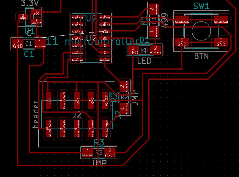
(Image 1) This is an image of the KiCad software telling me two components are not connected when in fact they are.
Note from Author
This is a reaccount of what happened this week because that is what happens in HTMAA. If you are in the ER, nobody cares and MIT life moves on, especially in this class. A new project is released every week so when I got behind on this week I had no choice but to move on. However, I do remember finishing shortly after the Wednesday it was due. Unforunately, I did not update my website for various reasons, which was a mistake. While I had some documentation lying around, I recommend just writing something up. Take 10 minutes to open up Notepad and just have a stream of consciousness about the week to reference later if you can't do the website update as soon as you finish the project.
Plan
The plan is simple. Redraw the D11C Hello World found here and add a button/LED. Nothin fancy because frankly I don't have the time nor do I have a some project that I can integrate with this assignment to bolster it (I've learned that a lot of people do this but I simply refuse to do this). Nevertheless, I was defintitely learning this week especially when it came to routing.
My logic for choosing the D11C was also simple. Firstly, I milled/sodered a D11C programmer in week 3 so I was familiar with those components and how to solder them (I can get a little shaky with soldering so this was important to me) Secondly, later in the semester there is a programming week and rather than mill another board, I'd rather save time by programming this board. By learning to program this board, I get a little experience with the SAMD line, which I plan to use for my final project.
The idea was to add an LED and button on one side of the MPU and simply extend the ground/power lines in Neil's routing (Image 1) to wrap around the small cluster of components I've added. Well, at least that was the idea.
Routing
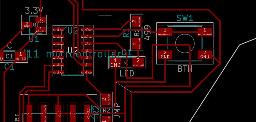
(Image 2) This is the work around to Image 1. The button is internally grounded so I routed power line under the button
This was my first time routing and boy was it unexpectedly tough. However, I am much more equipped to conduct routing after this experience. I have 2 tips: 1) You are smarter than the software 2) Use jumper resistors
In regards to tip 1, I made the mistake of thinking the software knew something I didn't. There was a component I needed to connect to ground, but to do so I needed to jump the main power line. So I added a resistor between a component output and a GND symbol in Eeschema KiCad (the schematic editor for KiCad). However, KiCad wants both ends of the resistor to go to different places. The concept of a resistor going from ground to ground didn't make sense to KiCad and so I would get different rat lines (lines that determine which component ends need to be connected via a trace) from what I expected when I opened my PCB layout editor after adding the resistor. These different rat lines prevented me from connecting my component to the main GND line so I couldn't just export the design in spite of the unfullfilled constraint.
So I wasted a ton of time on a workaround (image above), and when I say a ton I'm thinking like 6 hours. This was the main prevention of me completing this week's assignment on time. The workaround ended up coming from the fact that the button's GND pins were internally connected so there was no need to connect them via a trace. I was able to route a different signal through this opening which enabled a cascade of rerouting that allowed me to route everything I needed. The point, however, is that I needed to realize I was smarter than the software and add the resistor properly to the schematic to enable a jumper resistor (0 ohm resistor) on a ground line, which bring me to tip 2.
I have two methods for adding jumper resistors. If the jump is between two components (not gnd or power line), add the resistor by just snapping it into the existing wire in Eeschema. If not (as in my issue above), then add a resistor in "open space" and connect both terminals to a GND symbol in Eeschema. This was when you load the PCB layout editor, the resistor can go into any ground line. This may seem obvious, but believe that it was not at all obvious. The only tutorials that I saw in recitation involved the first method and the open space idea was new.
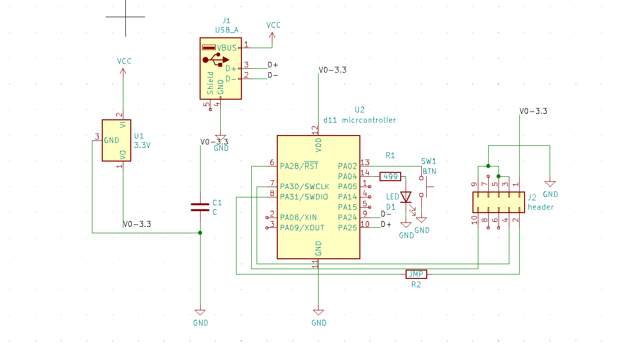
Anyways, the rest of the story is not that interesting. I completed the routing, milled, soldered, and tested with Anthony to check my electrical connections. The software I used to draw my circuit schematic and traces is called KiCad. Here are some project files (all pngs) that you may use freely: schematic, traces, outline.
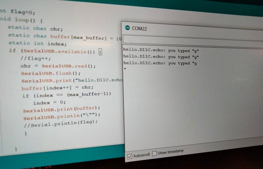
(Image 3) This is an image of my board sucessfully echoing a message