00 Final Project
For my final project, I've decided to do a transcranial alternating current stimulation (tACS) in a wearable system form factor. tACS uses electricity for neurostimulation at low currents and has recently been shown to induce particular sensations such as visual and auditory sensations. Coupling this technology with various input sensors could provide a way to directly alter human sensations as well as help promote superhuman awareness in loud and dangerous environments like factories.
Safety Precautions
Since neurostimulation uses electricity applied directly to the cranium, there are potential safety related risks with developing such systems. The amount of current a person can tolerate and still be able to control his or her hand and arm muscles is less than 10 mA, while currents above 50 mA causes extreme pain, respiratory arrest, severe muscle reactions and can lead to death [1]. For electricity applied directly to the head, currents up to 5 mA are typically used in commercially available devices such as the "1x1 tES", "nurostym tES", and "Neurostim tES". Low-intensity transcranial electrical stimulation (tES) has been used in thousands of studies without serious adverse effects being reported, and its safety is well established for conventional low-intensity tES, in which peak currents do not exceed 4 mA and stimulation duration is kept under 60 minutes per day (Antal et al., 2017). Moderate adverse effects are rare, and for normal healthy subjects usually consist in skin lesions, but most adverse effects are mild and disappear after stimulation. Particularly for tASC, no persistent adverse effects have been reported (Matsumoto & Ugawa, 2017).
To further assess the safety risks of developing a tACS system, together with technical intructor Tom Lutz, I got in contact with MIT Environmental Health & Safety (EHS) and MIT COUHES. These were the particular recommendations from EHS.
- 5 mA output max. A buffer or similar should be used to ensure no more than 5 mA comes out.
- It would be good to include a current sensor in the design
- To evaluate current outputs, an oscilloscope and sensitive multimeter can be used.
- Find a good way to simulate the use of the device with a model (like fake skin) before using it on a human.
According to COUHES, "the work does not meet the definition of research" at this stage and hence "COUHES review is not required". However, if I were to begin gathering data for research purposes, I would need to submit an application for review.
Electronics Design
In general, medical tACS devices consist of the following basic components which perform specific functions:
- Power source: External battery ensures isolation from electrical grid while making device portable.
- User interface: Allows users to choose operating mode, amplitude, frequency and other program settings.
- Microcontroller: Processes user inputs, controls other components and stores data.
- Waveform generator chip: Converts digital signals from microcontroller into a variety of waveforms (e.g., sine, triangle, pulses) with precise frequency and amplitude.
- Voltage controlled current source: Transforms voltage input in current output, ensuring current level even as electrical resistance between electrodes vary and isolating input and output.
- Safety circuitry: Electrical buffers are used to create additional layers of isolation between input and output, current limiters ensure that maximum current levels are not exceeded and fuses act as a failsafe. Additionally, current sensors
- In order to be able to control the signal with sensor data, I intend to build my own tES device, with identical electrical characteristics to the commercially available devices.
- Electrodes: Transport electric current to the patient’s head and distribute current across skin.
For my implementation, I knew from the beginning that I might not have the time to implement a battery power source as well as user interface so they were put on the "nice to have" list. For the rest of the components, I learnt that you can use the digital to analog converter (DAC) on various microcontrollers to generate waveforms making a waveform generator chip obsolete. Further, generating the voltage waveform on the microcontroller would also allow me to change the max voltage in the software. For the voltage controlled current source, based on a previous project, I found that the LM1370 operational transconductance amplifier (OTA) is a common OTA that should work nicely.
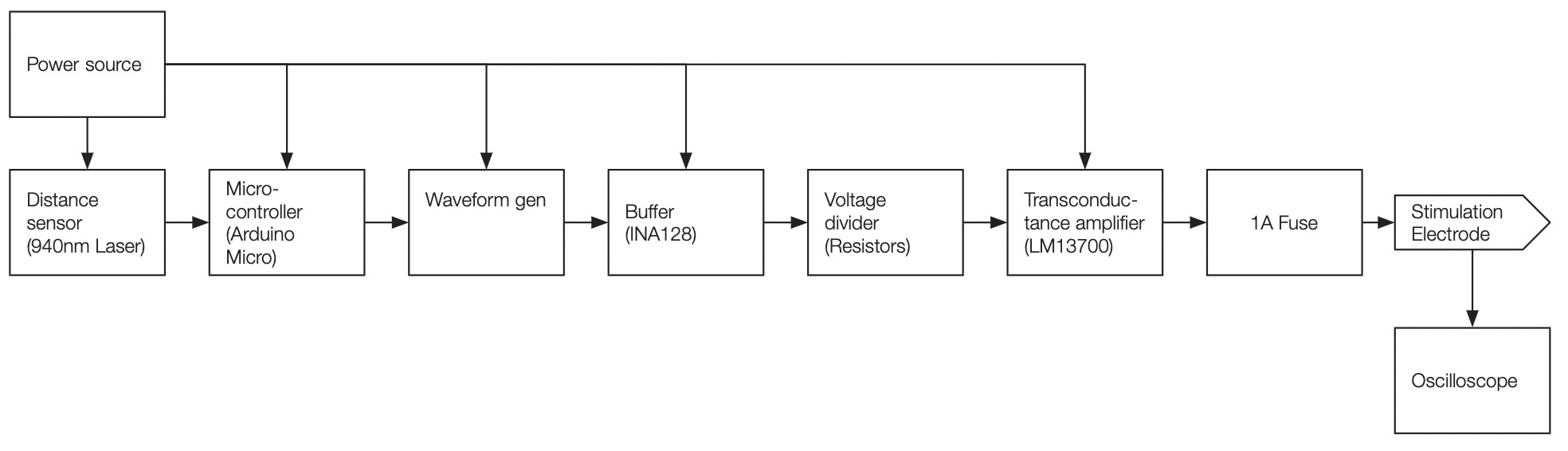
On top of the standard tACS devices, I wanted to add a sensor input to be able to use the sensory outcomes of the stimulation to augment the users spatial awareness if their surroundings. Adding a time of flight (ToF) sensor in the back of the headset would potentially allow for controlling the frequency of visual sensations elicited by the tACS system. For the ToF sensor, I bought the SparkFun SFEVL53L1X ToF sensor. The block diagram of the system can be found below. Based on the block diagram, I ended up only needing to build a circuit with three separate components: the microcontroller, the OTA with output current for stimulation, and the ToF sensor.
ESP32 Microcontroller
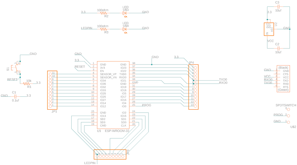
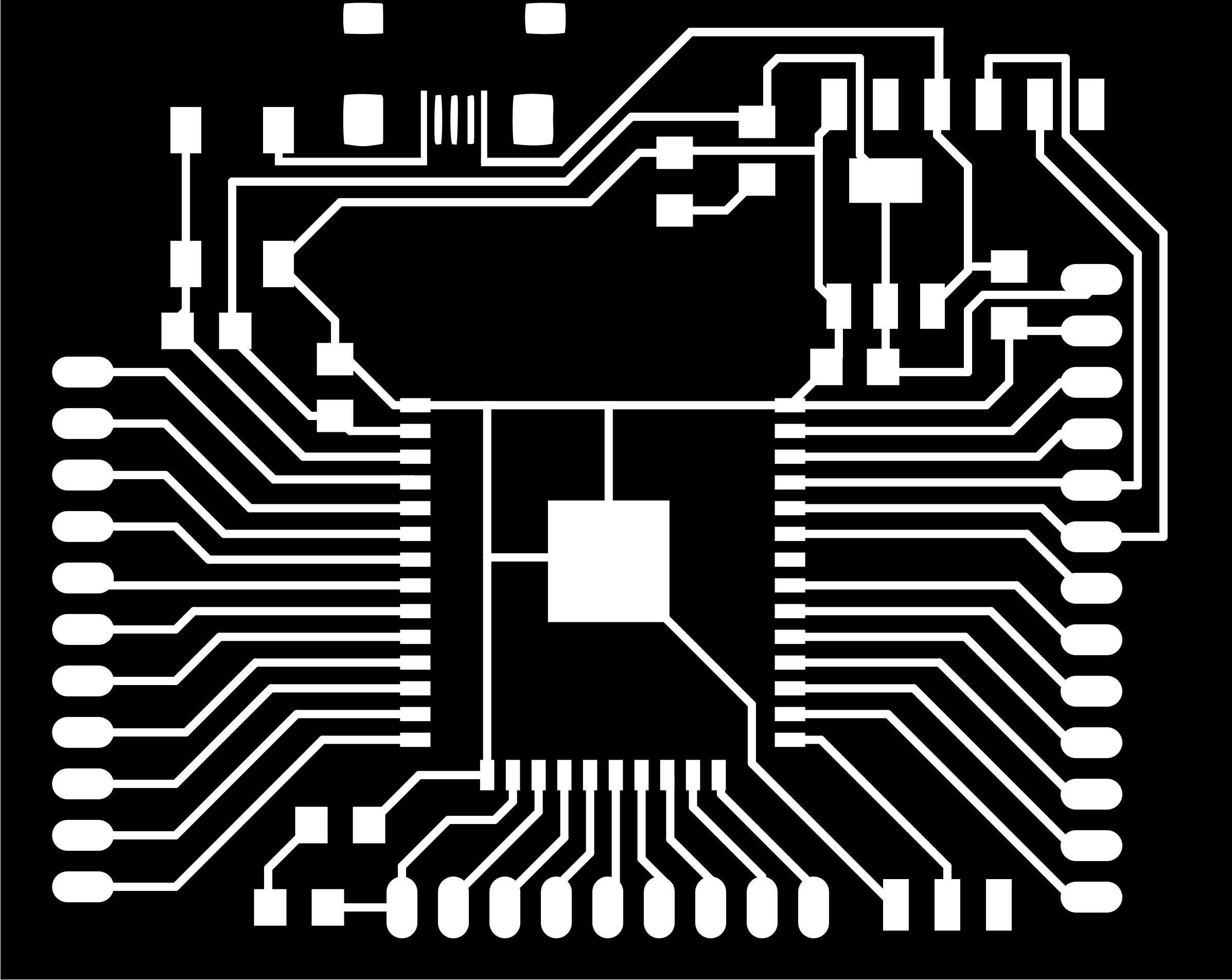
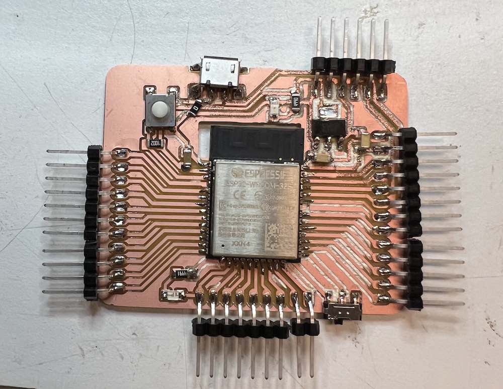
The ESP32 microcontroller has a digital to analog converter. Further, it is also more way more powerful than the SAMD11 used in my previous circuits which did not have enough memory to work with float values for generating a wave function (see week 09). In addition, it also has digital to analog pins that would allow me to read my output signal from the DAC and verify that the waveforms are coming out nicely. Due to the issues I had with my own ESP32 board in week 10, I designed an ESP32 devkit breakout board in Fusion360 based on the design of the open-source Barduino 2.0 board and added a micro USB component. This allowed me to power the device separately from a computer (see schematic and exported traces below). Then, on the Roland SRM-20, I started milling the PCB for the ESP32 Microcontroller and then proceeded to stuff the board. I then set the board up following this guide.

Waveform Generation
The waveform generation was done using the digital to analog converter (DAC) in the ESP32 in combination with software running on the microcontroller. Based on the ESP32 datasheet, I found that both pin 25 and 26 had DAC outputs allowing for output voltage between 0-3.3v. Based on simulations of the operational transconductance amplifier used (LM13700), I needed one DAC to output an the voltage waveform between 0-2v and another DAC to output a DC voltage of 2v to avoid the LM13700 causing distortion in the waveform output. For the waveform generator code, I used the Function Generator library. This allowed me to define a waveform, frequency and amplitude for the waveform. Waveforms included common neurostimulation waveforms such as sinus waves, triangle waves, square waves and random noise waves. Below video shows serial plots of the triangle, sinus, and square wave functions run together on the ESP32. The output waveform voltage was then output on pin 25 and the DC current matching the max waveform voltage (2V). Code will be available on GitHub soon.
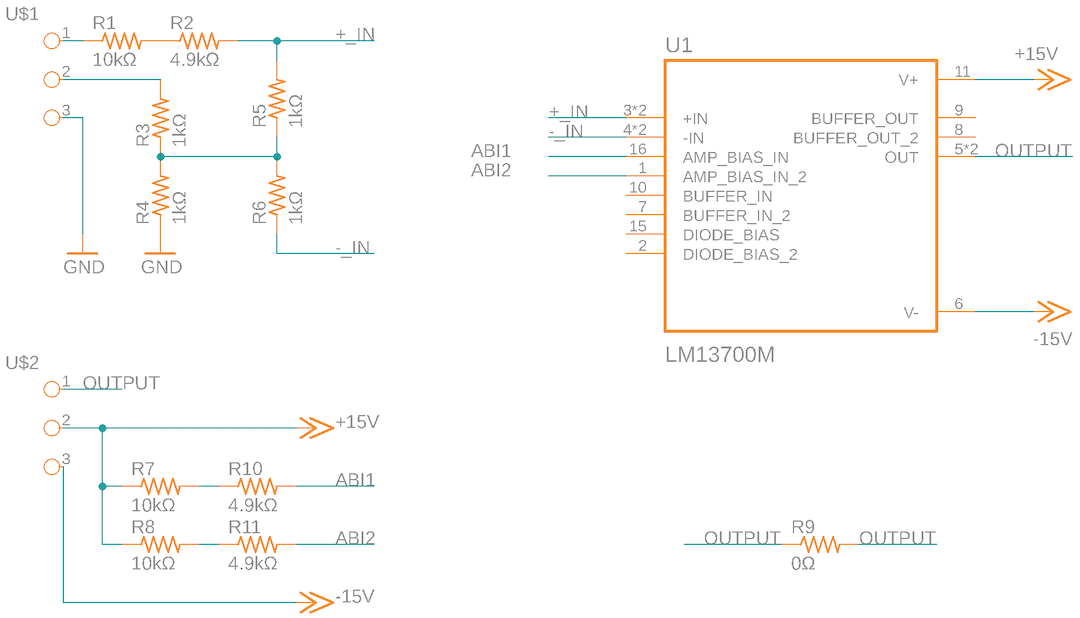
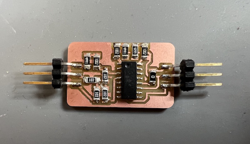
Operational Transconductance Amplifier
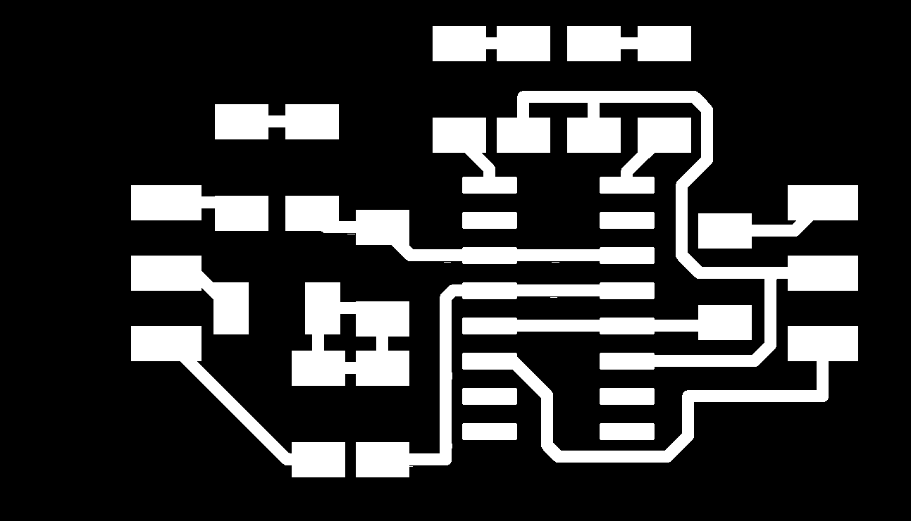
Operational transconductance amplifiers (OTAs), capable of generating voltage controlled current output, are an amplifier whose differential input voltage produces an output current. The benefit of using OTAs is not just about translating the voltage waveform from the DAC to a current waveform but moreso its capability to keep the current output unaffected by varying impedances. In order to properly determine what inputs are appropriate to reach an alternating current output between 1.5mA to -1.5mA following the DAC waveform, I talked to Mark Feldmeier from the Responsive Environments group at the MIT Media Lab. Together, we arrived at the following schematic for the OTA.

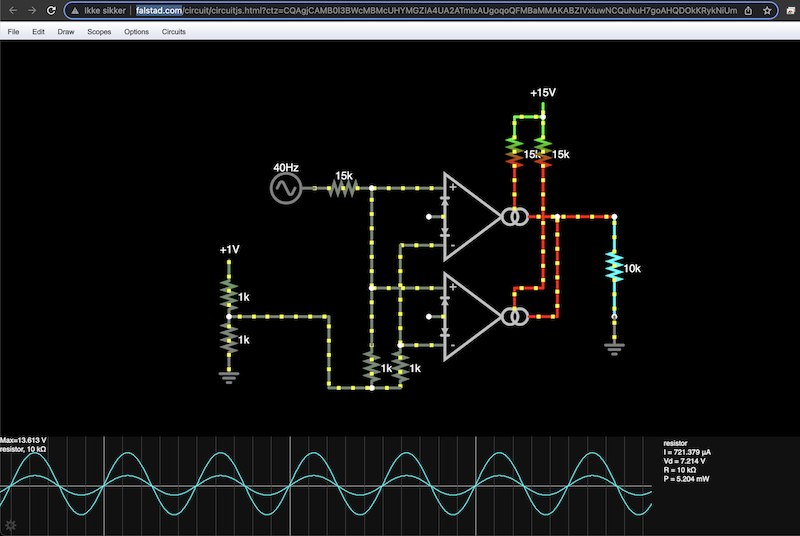
Evaluation Using Simulations
The schematic was based on simulations done in Falstad. Running simulations in Falstad allowed us to evaluate the current outputs with changes in impedance. Generally human impedance is around 10kΩ. We found that the current outputs were unchanged with impedances 2.2kΩ to 15kΩ. Higher impedances made the current output decrease. From these simulations we concluded that the prototype was only able to output human safe current levels. See a snapshot of the simulation below.
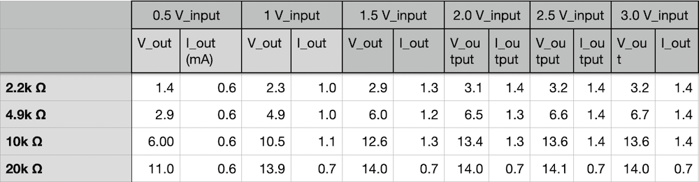
Evaluations with Oscilloscope
With the breakout OTA board stuffed, I connected it with the AC waveform voltage and DC outputs of the ESP32 board. I also used two power supplies with +15V and -15V respectively for the OTAs supply voltage requirements. The +-15V would limit the current to not exceed 1.4mA. With the boards connected and a 10k resistor dummy (representing the human user's impedence), I was able to measure consistent sinewave voltage outputs on the oscilloscope with the correct defined frequency (10Hz).
Varying the input voltage to the OTA manually, I logged the consequent voltages and current outputs across differences in resistance and voltage input. I found that empirically the current output stayed invariant with changes in resistance under 20kΩ. I also found that, as expected, changing the input voltage resulted in different current outputs, allowing me to output various levels of intensity. Lastly, I found that the current started to plateau at voltages above 1.5V. See the table below for the empirical results.
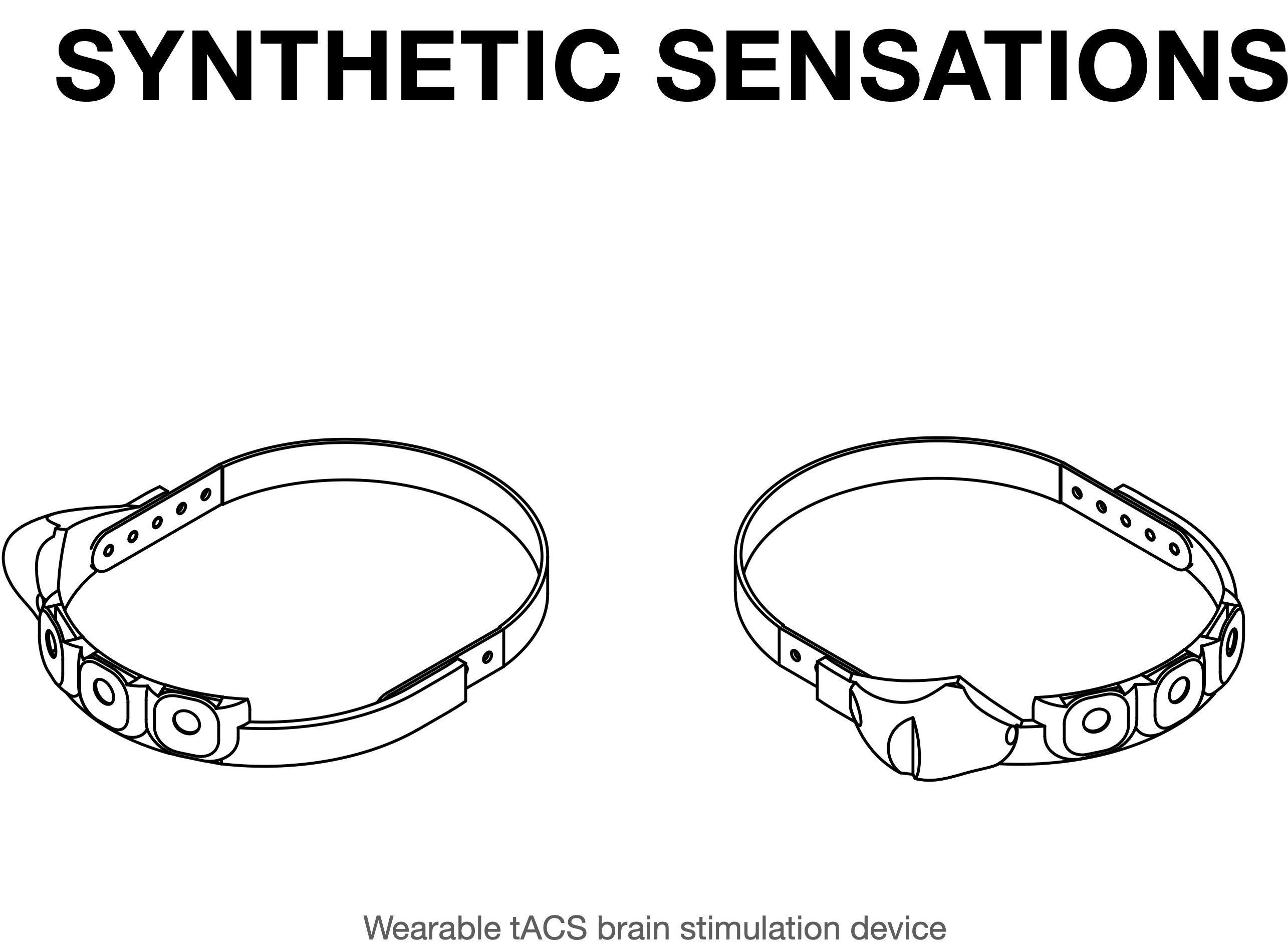
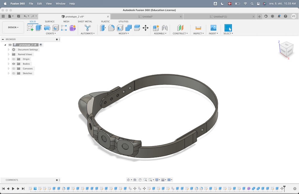
Design of Wearable Housing
I imagened the final form factor of the stimulation system to be a compact wearable headband. After measuring my own headsize, I started sketching out a simple design for the wearable in Fusion360. Satisfied with the design, I 3D printed the wearable on a Formlabs Form 3 printer with Preform. Find a picture of the Fusion 360 design below.
Final Prototype
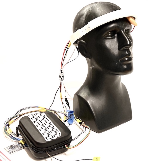
Finally, I combined all the steps above into one integrated design containing both the electronics, wearable design and wet sponge electrodes. I had to buy the wet sponges and make sure that the end of the cable fit into the wet sponges. I also bought saline solution to make the wet sponges conduct better. Find an image of the final prototype below. For future versions of the system an integrated PCB without breakout board components will be designed. The electronics in a future version will also be housed inside the wearable to avoid long dangling cables.