04 Electronics Design
AI AMULET

[DISCLAIMER: Unfortunately I was sick for an entire week which halted my progress...]. I later went back to this week (around week 9) to complete the assignment.
For this week, I wanted to build a simple blink device and have the blinks be morse-code of something. To develop the concept around what my circuit board might conceptually be, I used Open AI's text generation model, GPT3, to generate concepts. Asking the AI model what would be a good outline of my PCB, I got the output that the morse-code device would be a "mystical amulet".
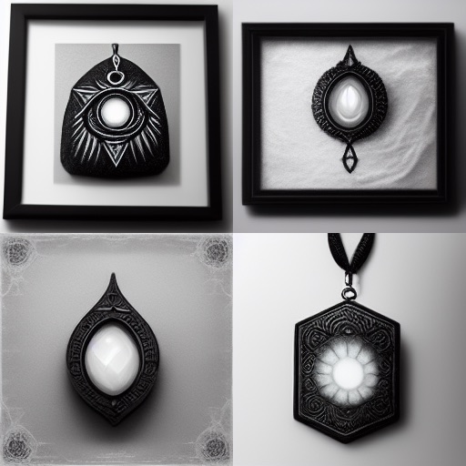
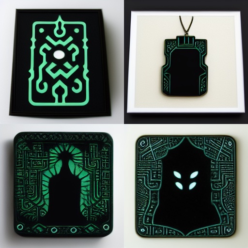
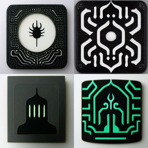
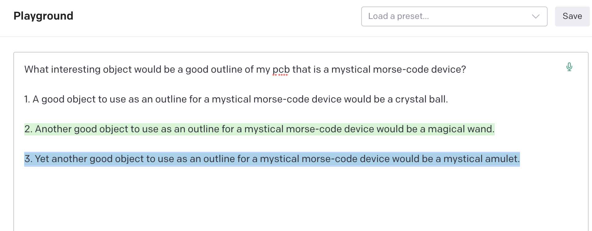
From the idea of the morse-code device being a mystical amulet, I fed this text prompt into the image AI generation service "Midjourney" and generated potential PCB board designs. The prompts were "mystical-amulet-black-on-white-background", "mystical-circuit-board-amulet-black-silhouette-on-white-background", and "mystical-circuit-board-talisman-black-silhouette-on-white-background". I chose to go with the green necklace amulet.
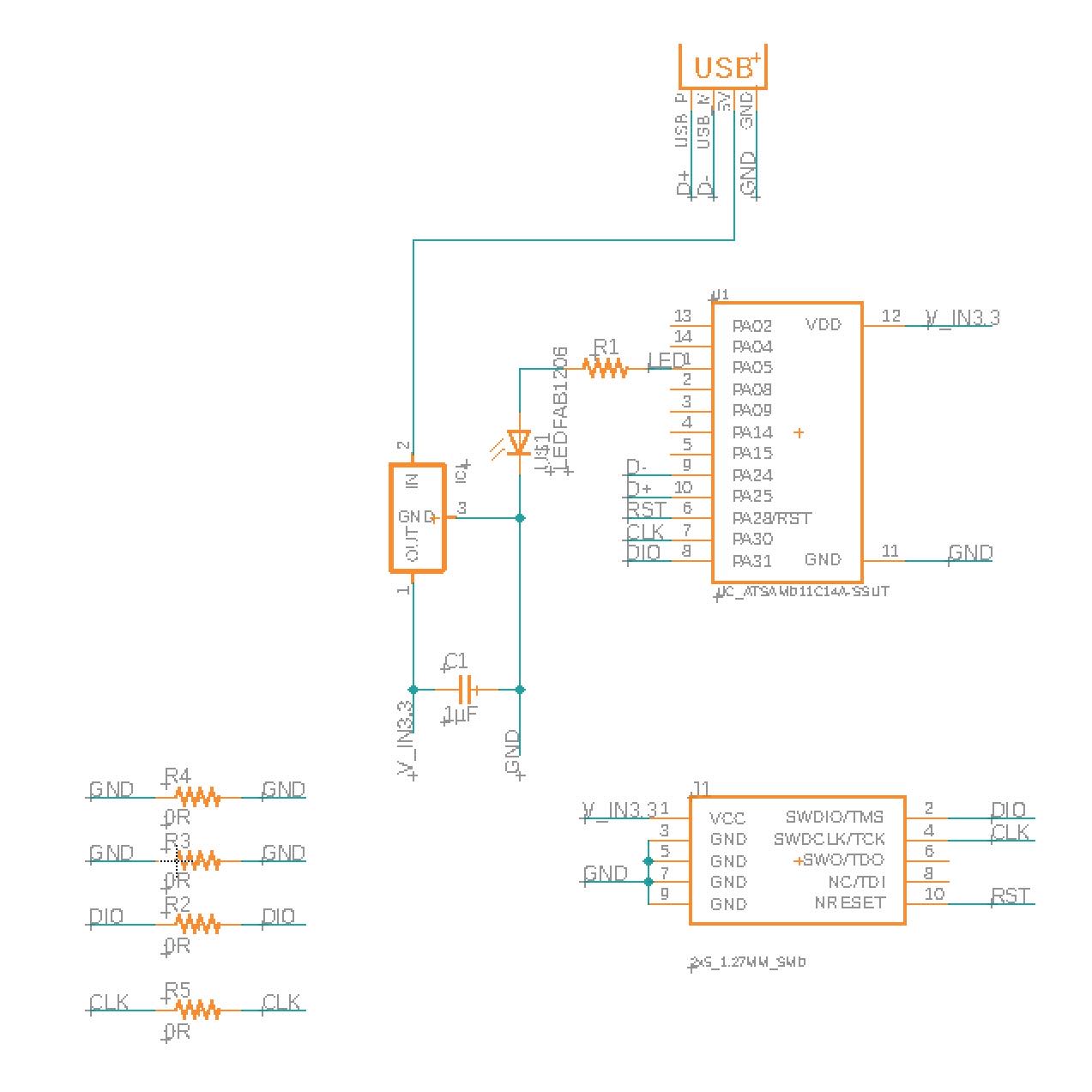
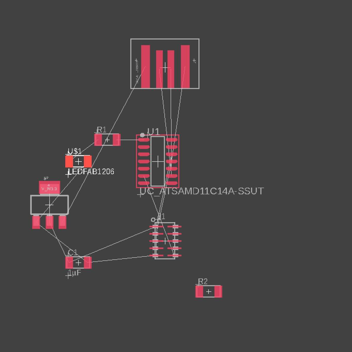
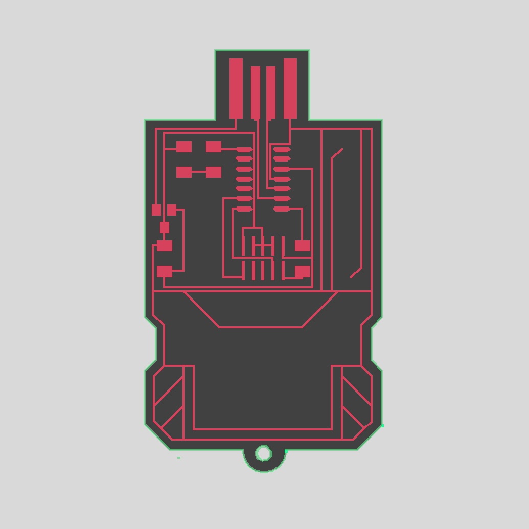
After a bunch of tutorials on Youtube to understand the fundamentals of Electronics design (such as capacitors and resistance), I began using Fusion 360 Eagle to recreate Neil's blink board design. First, I found all the components in the library. Next, I had to net the components to ensure that they all got the proper input voltage, were connected to ground as well as each other in the proper ways. I chose to use the microcontroller SAMD11C14A which uses an input voltage of 3.3V. I used a voltage regulator to change the voltage to 3.3V, attached an LED to pin "PA05" with proper resistors, and attached a 5x2 JTAG header. When the components were added, I routed all the components properly. After spending a few hours on components and routing, I had not saved my progress and Eagle chose to randomly crash on me. This meant that I lost all my process and had to start from scratch. When I had routed all the components properly, I made sure that the design followed the AI generated image design.
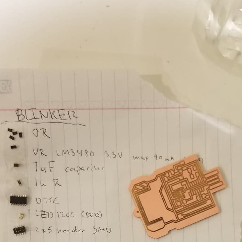
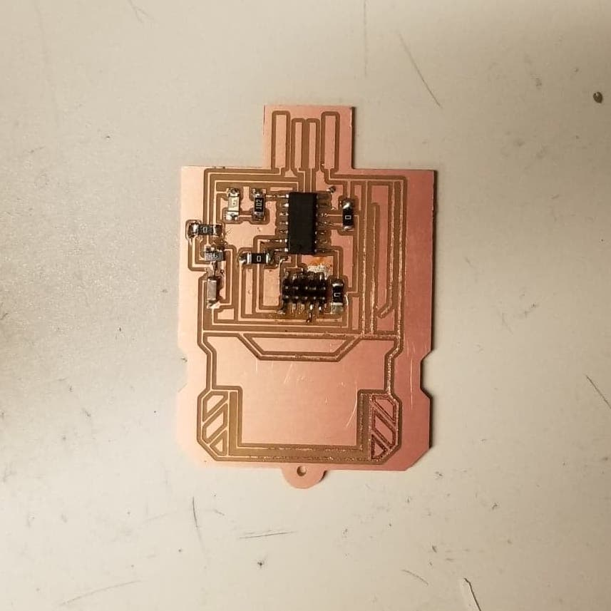
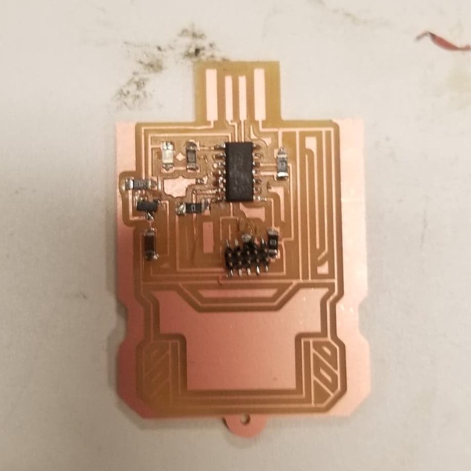
After the board was milled, I then started collecting the components for stuffing the board. I then soldered the board. During the soldering process, I practiced using copper tape to remove solder. With the stuffed board, the tried to install the bootloader but kept getting an error. I then tried to remove the connector from the board, and that broke the board... I then spent 2 hours re-milling the board and stuffing it again. I still could not install the bootloader successfully, and when I tried to remove the connector from the board -guess what-, I (again) ended up breaking the board apart... I suspect that the PCB traces were too tiny for the JTAG header connector. For the future, the design will feature wider connector copper areas to enable a stronger soldering.