Week 4 - Electronics Design
Preface
Remember Week 2? I said I might design a PCB for my bathroom door. Here is my chance. The goal of this week is to use an EDA tool to design a development board to interact and communicate with an embedded microcontroller. I want to carry over the functionalities of my original circut while implementing bluetooth. Prior experience designing circut boards? None.
Learning Electronics Design
After the introduction of many tools for EDA in recitation, I decided to pursue Fusion360 and Eagle. The electronic design aspect of Fusion360 seems like another big challenge in Fusion360 to tackle and will continue to build my proficiency with the software. I began by mimicking the RP2040 design Anthony builds in recitation. For some reason all my parts are red compared to the yellow lines in his drawing.
My first electronic design is to bring my circut board from week 2 to Eagle. It looks pretty good to me. I wired it like how I wired my breadboard but for some reason the PCB document looks a little weird. Nothing is going to ground? In the process of debugging, I realize that I will actually learn more if I design a board that takes in the full functionality of the ESP32. Especially since I will need two of them for my bathroom light idea to work.

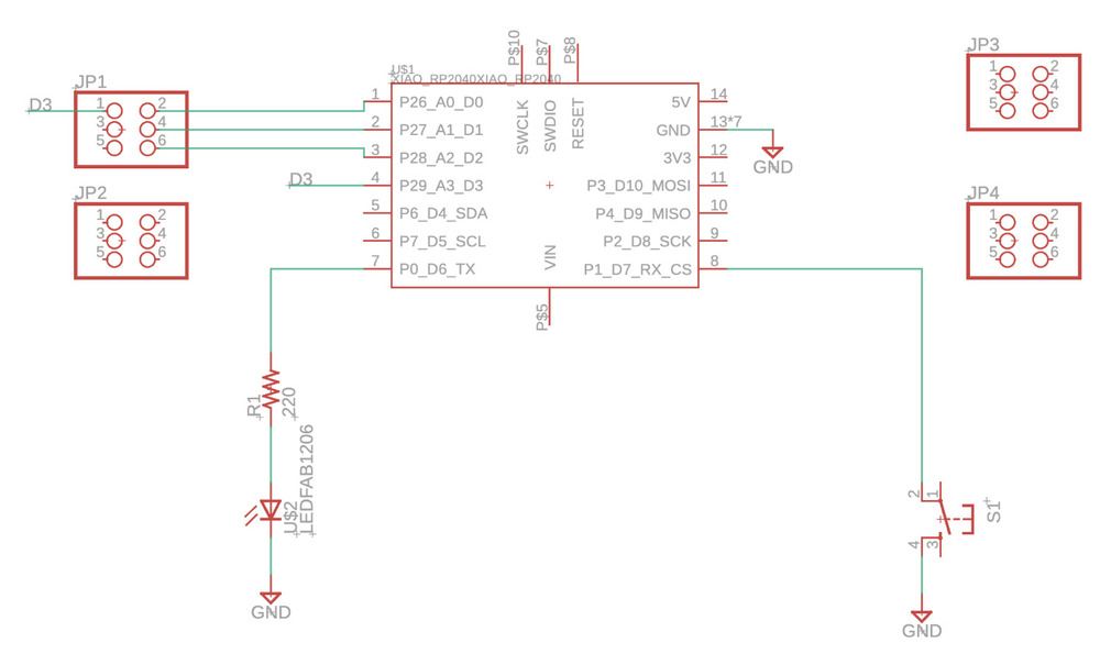
I was able to get a schematic for the “Fab-Xiao” from Adrián Torres. I downloaded the .sch file and opened it in Eagle. This schematic was made for the Xiao RP2040 but the introduction mentions that it can also be used for the ESP32-C3. Using this existing design, I will modify it to fit my ESP32-C3
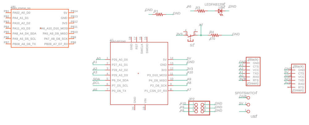
ESP32-C3 on the left, schematic of Fab Xiao with RP2040 on the right
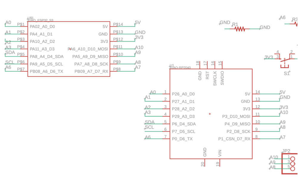
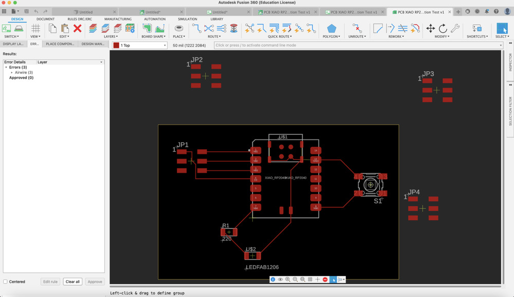
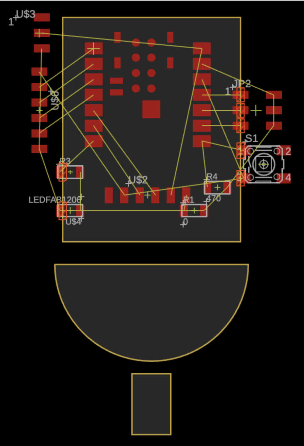
I copied all the names and put on nets on the ESP32. Then I deleted the RP2040 and viewed the mess in PCB mode.
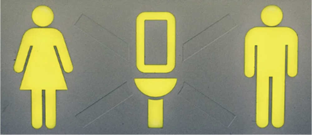
I found this neat airplane bathroom sign from Getty Images. But I think I will just take the middle and sketch my own SVG.
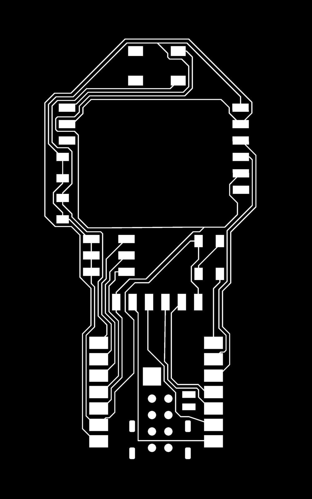
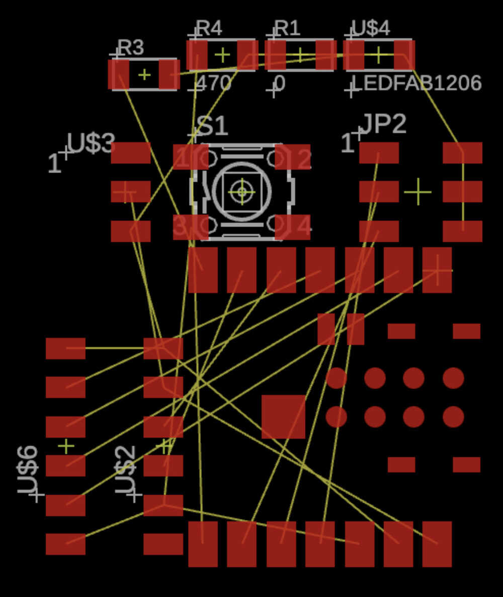
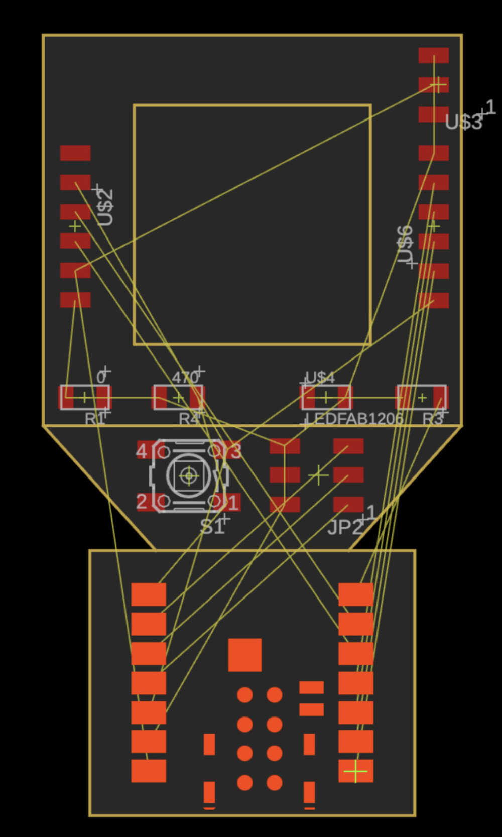
Let’s try to fit the PCB into the toilet design! I moved the components around generally and traced the board shape with outline polyline and outline arc in the PCB design. Then I realized that I want the USB-C at the bottom so I will reorganize everything.
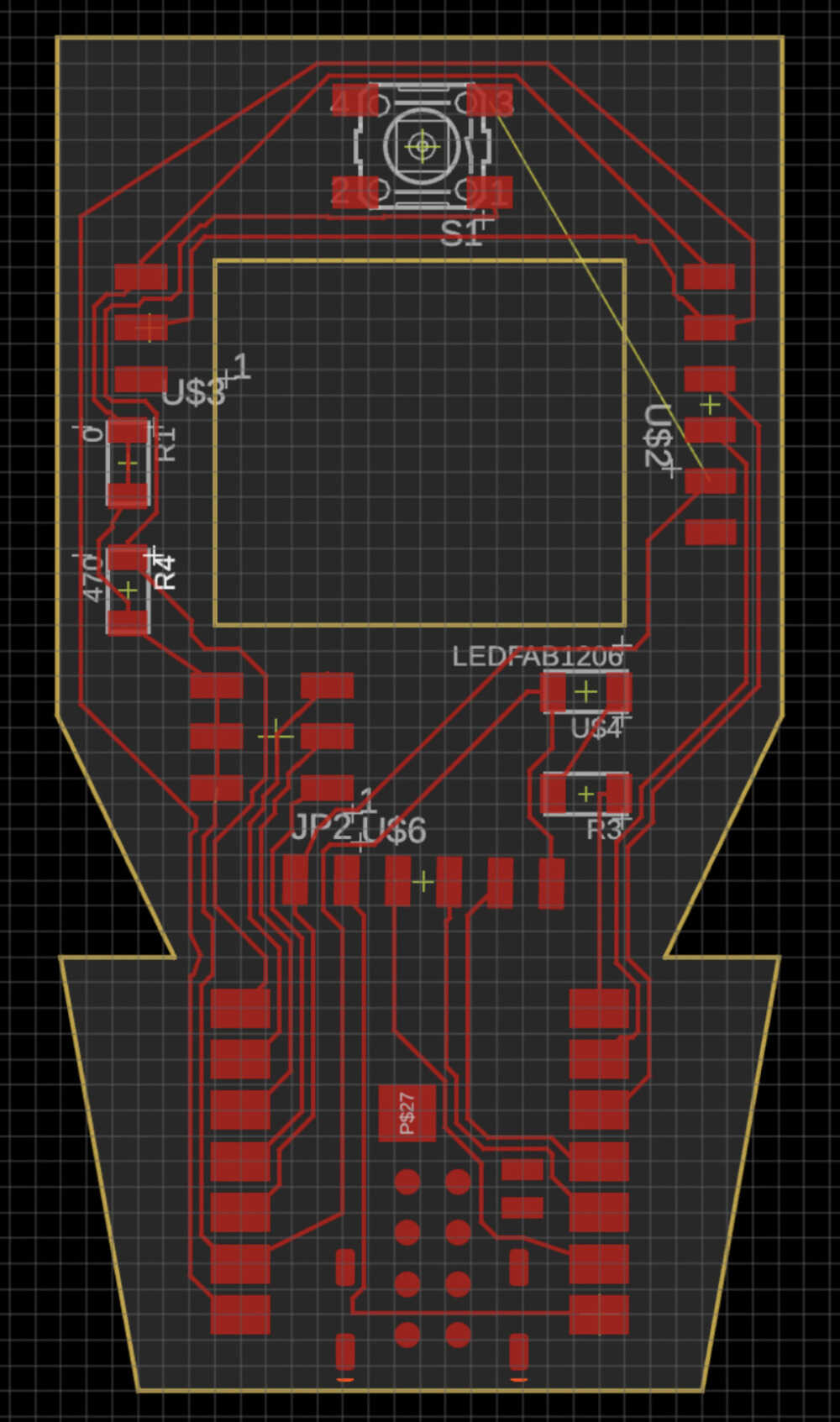
Curve sketching was a little wierd in PCB Design page so I made another version of the toilet.
I’ve spent so much time thinking and wiring everything. It has been kind of fun. Before I started messing around with everything, I changed all clearance to 16 mil. One trick I learned is that I can give connections a lot of space and then move them tighter using the arrow keys. Another thing I learned is that the yellow lines can be deceiving sometimes. Once I click onto the connection using route manual, it will show me all the parts for that connection to link, so I can actually pick another one that might be easier to wire. One connection left!
Finally! Woo!
To export my design, I followed the guide from Jake’s ECAD Demo.
Week 4 Final Thoughts
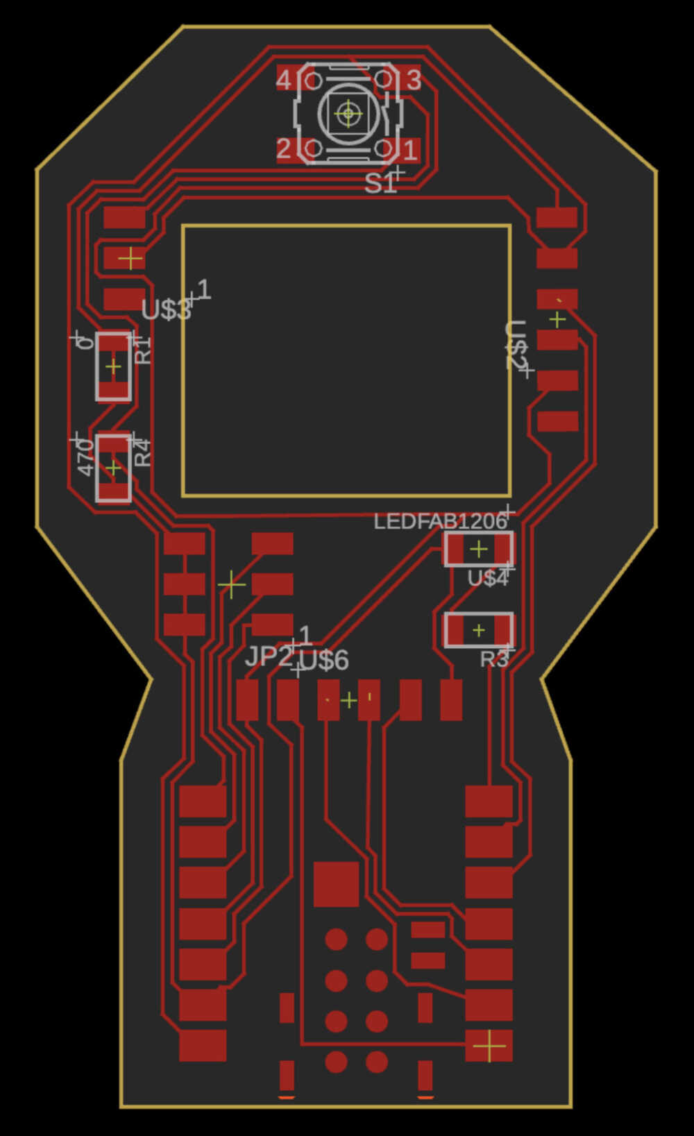
Here are my designs ready for fabrication next week!