A personalized board with a button and an LED.

Eagle
To design the board, I used a free (sorta) software called Eagle. It is pretty straightforward, especially when you have a library populated by past MAS.863 students for components. Eagles has two big views; Schematic and Board View. Before starting, get the library from the class repository. The Fab library has all the components you will need. Finally, before you start, get familiar with all the Eagle buttons. The hardest part about Eagle is all the ridiculous amounts of buttons that are necessary to do simple tasks.

Schematic View
In schematic view, you link all pins of all components using a "net." A "net" is a visual link between pins that provides guidance when you go into board view. You can also add labels to nets. Nets with the same labels are automatically linked (not necessarily visually in schematic, but definitely in board view). As you add components from the library, right click to rotate the component by 90 degrees before placing it. When the "net" is active, right clicking with make turns on the path. Also, once you connect a net to a component, when you move the component, the net will move with it.
Below is my schematic. It has a a button (switch), ATTiny44a, an AVRISP, a 1uF capacitor, a 20 mHz crystal, two LEDs, 3 10 KOhm resistors, 1 0 ohm resistor, and one FTDI header.

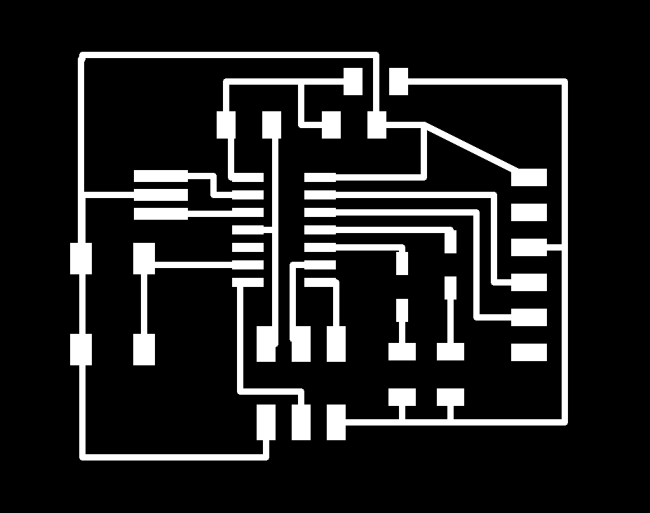
Board View
First of all, to get here, press the button on the top horizontal toolbar, not on the left toolbar. In general, when working in board view to design your board, you want to group things close enough to not waste material printing/milling, but far away enough to be easy to solder. Remember to give enough clearance between end mill paths. The Modelo machine has a 1/64 inch end mill (15.625 mil), so use at least a 16 mil clearance.
The main point of the board view is to use the route tool to remove the yellow lines (electrical connection) and replace them with routed (red) lines. Generally, space out your components how you would like them, and then start routing pins together. Remember that you can route lines in between leads of components.
Finally, before finalizing your board, use design rules. The fab library has a design rule library. To use it, the button is on the bottom left. Along with some other things, it will check distances of end mills and tell you if the board is millable.

Exporting
The outer line you see is just the dimension layer, not actually the physical circuit board layers. Dimension layers just control what you are exporting. To create the millable area, click the "rect" button, then select the milling layer (layer 46), and create a rectangle around the entire circuit.
To finally export, go to layers and only show one layer at a time. For the traces, show only the top layer ("display none top"). Go to file, export, select image, be suer to select monochrome, use at least 500 dpi, and then click ok. Do the same thing for the exterior trace (use "display none mill" to display that layer).

Production
In order to create the board, I followed the steps from one of my past weeks on Electronics Production. As in before, you start with a checklist. However, this time, I accidentally used a 1/32 inch bit for my traces because someone left a 1/32 bit in a 1/64 box. Being the noob that I am, I did not notice haha. It wasn't until 2 hours and 3 iterations of spacing my routes out later when I switch the end mill because it was not sharp anymore that I compared the two and realized this.


Anyways, I was finally able to mill my board and stuff it with components. I accidentally scratched my board at one point, so I used a voltmeter to ensure all routes were still continuous. Turns out they were all good.


And finally, the final board!
