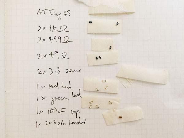
Electronics Production
This week was a relatively straight-forwardly technical, with less emphasis on design. The aim was to make a FabISP programmer from scratch: milling the PCB, soldering the components and programming the programmer (so that it can programme more programmers).
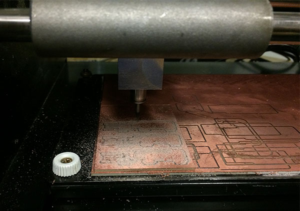
Steps to milling the PCB
Preparation: Open the server. It should display "status:socket open"; use "move to origin" to see if the machine is responding, and to set the origin point.
On the SRM20, if the lid opens when the machine is running, it will stop the operation. Use the Roland software to resume the programme that has already been sent to the buffer. The Roland software (VPANEL) will also tell you the exact position of the endmill.
Fixing down the material: Use doublesided tape (making sure material is clean of old tape). The board must not be at an angle. No dust on the plate, no doubling of tape, bubbles etc - as long as it looks and feels flat it should be OK. If it isn't flat it may break the endmill. Try to orient material so that three widths of the PCB can fit down its long side.
Get endmill holder and tighten the set screw with tool shank; the screw applies clamping force to the side of the tool. SRM20: there is another hole on the other side of the set screw. UBUNTU MACHINE: there are 2 set screws. Slide the tool up into the shaft as far as you can, and tighten the set screw gently.
Make sure endmill has a straight head and is not broken (sometimes broken ones end up back in the box). Don't drop the endmill, try be aware when the tip is, it's fragile.
Set the origin: Default origin is 10x10x10px. Set the x and y co-ordinates until it's at the front left corner of the material. Use the side window the check y axis. To set the z co-ordinate, loosen the set screw and hold the endmill so that it doesn't fall. z is the surface: just make sure endmill is resting on the material. Tighten the endmill. On the Ubuntu machine, use the UP and DOWN buttons to move the endmill.
Send the code: Hit calculate on "mill raster" to generate the PNG toolpath. Hit send to device. You may need to change the cutting depth slightly, but more likely the endmill or flatness isn't right.
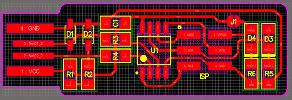
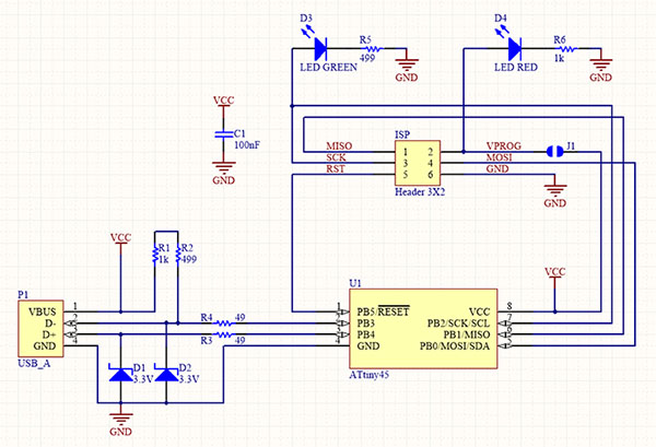
Soldering the boards
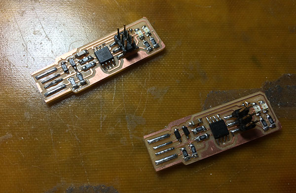
The next step was to solder the quite small components onto the PCB. Once the components were assembled and the board tacked down with a little masking tape, the soldering was actually relatively painless. What caused me problems was my basic grasp of electronics. Once I forgot to orient the processor chip using the small lasercut dimple in the corner, and twice I put the diode down the wrong way around (anode --> cathode!). Quite a pain to desolder using the braid, especially since these PCBs were not the most durable. In my attempts to desolder the six legs of the ATTiny45, the plastic began to melt, dissociating itself from the copper.
These hitches aside, I soldered two FabISPs without issue, and was relieved to find that the red LED came on when I plugged it in, at very least. In order to make the connection a little stronger, I took Neil's advice and applied some extra solder to the USB connectors, as well as cutting off a little square of packaging plastic and attaching that to the underside of the USB connector to give it some slightly more substantive padding.
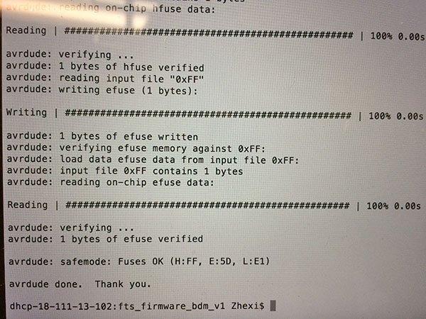
For some reason I had some trouble using the architecture shop's Ubuntu machine and programmer to configure my ISP, but I was later able to follow Brian's instructions to do so on my Macbook.