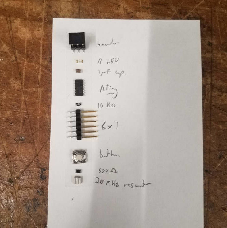
Echo Hello World Board
This week was another one that required less creativity, but it ended up being a really good one for mistakes. We were tasked with modifying an echo hello world board with a button and LED -- they don't have any functionality yet, but I'll add that in two weeks.
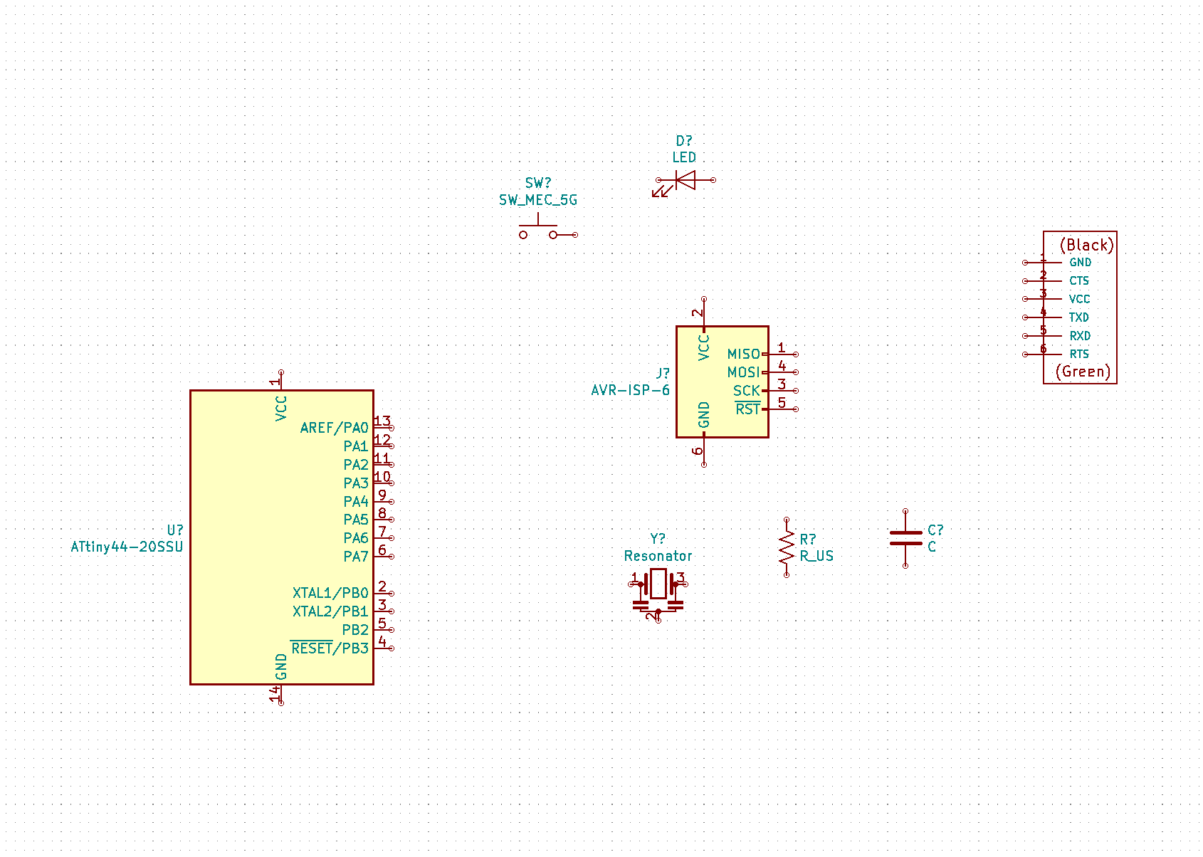
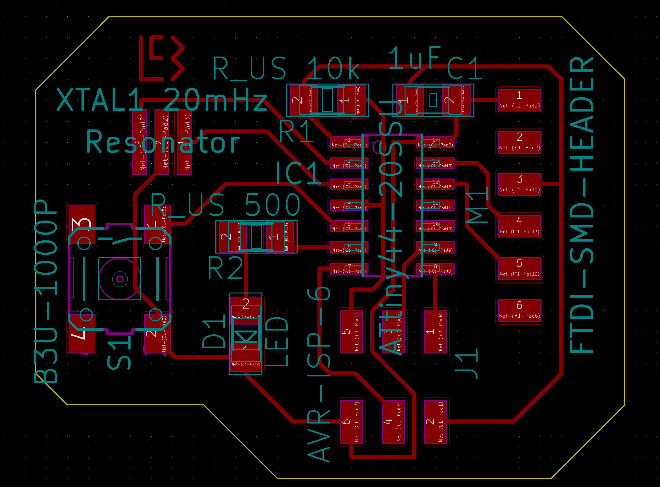
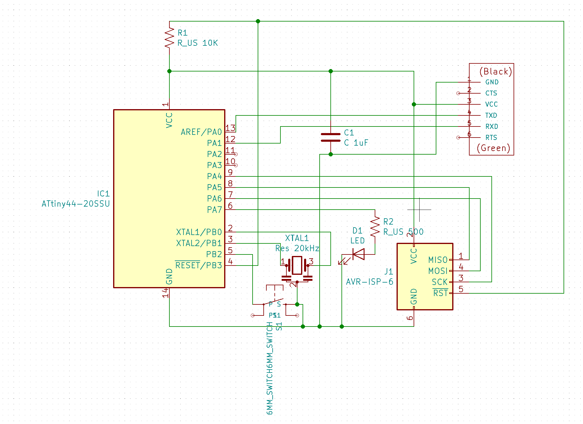
To begin, I remade the schematics of the original echo board. I used KiCAD, and had a bit of trouble managing the libraries I downloaded from DigiKey and the fab repo. I eventually found all the right symbols and drew out the connections.
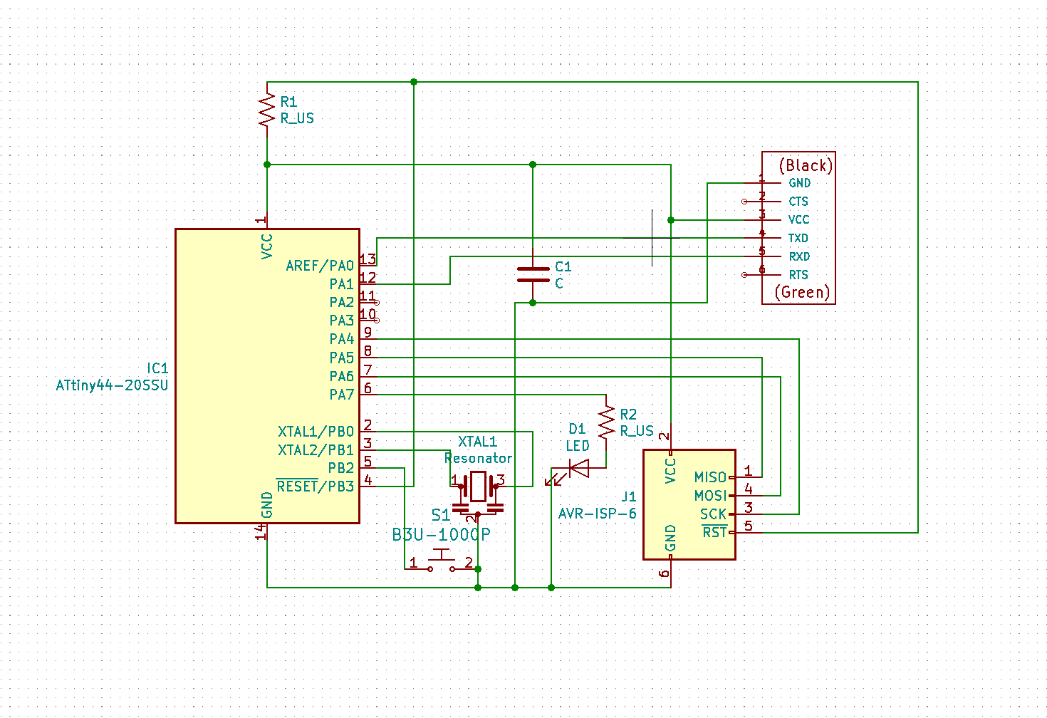
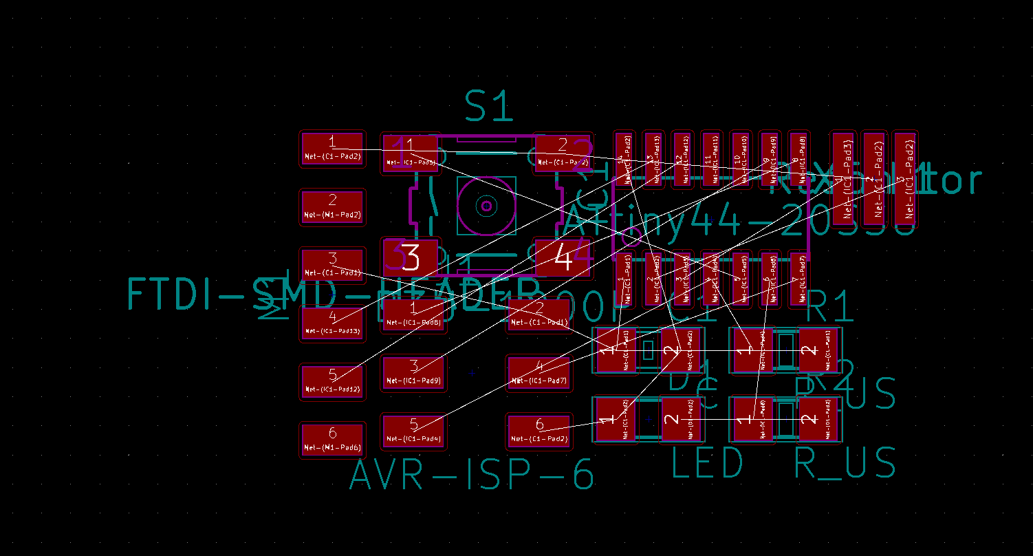
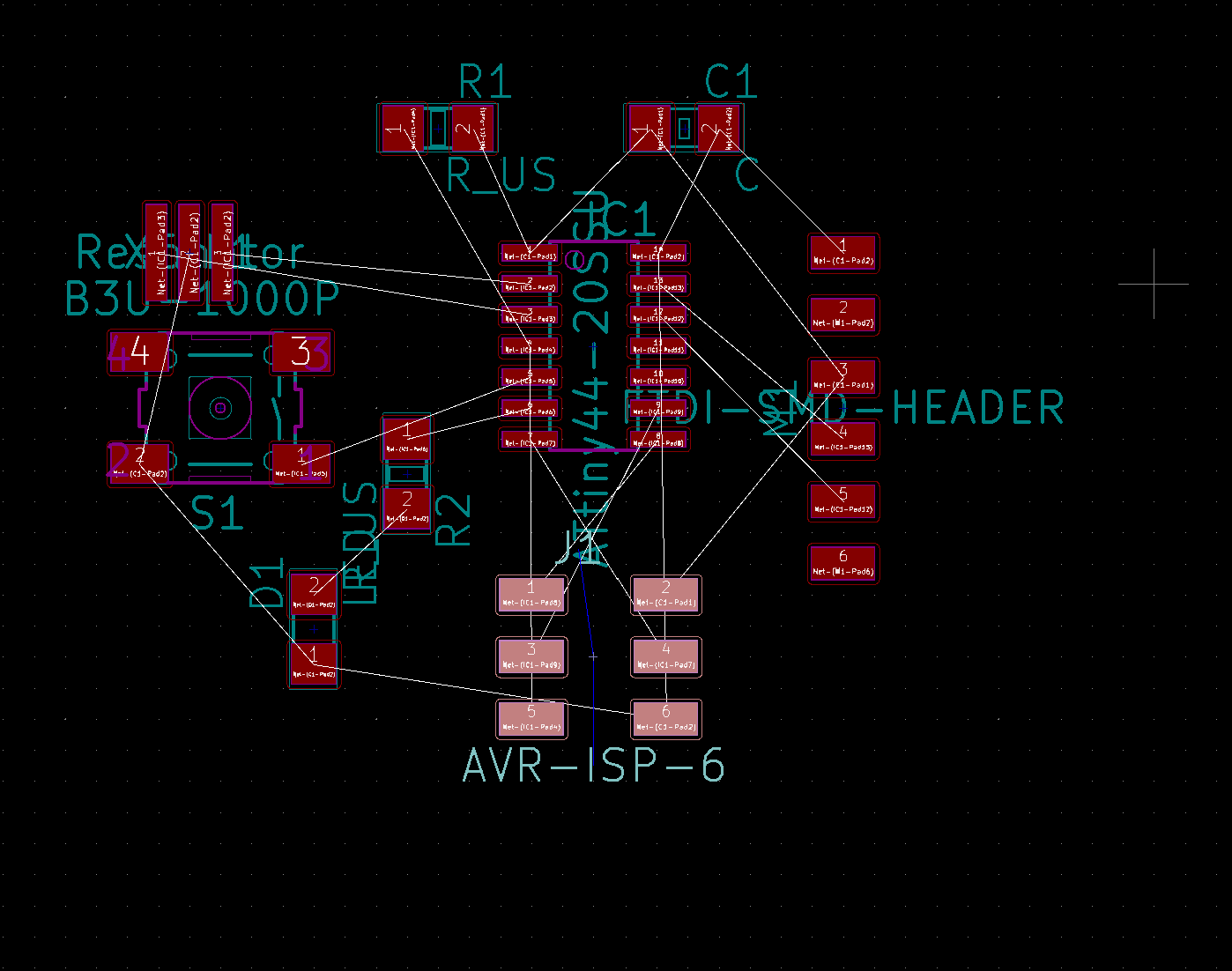
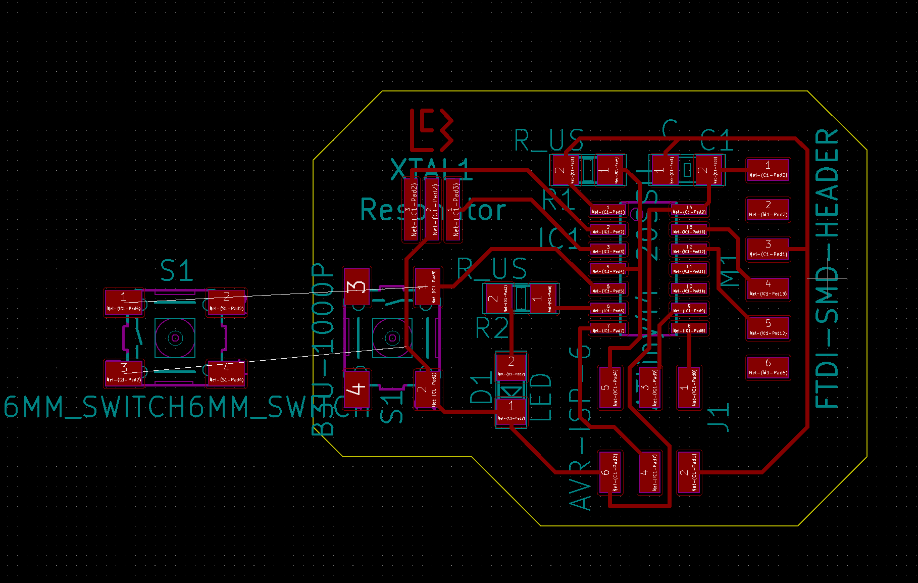
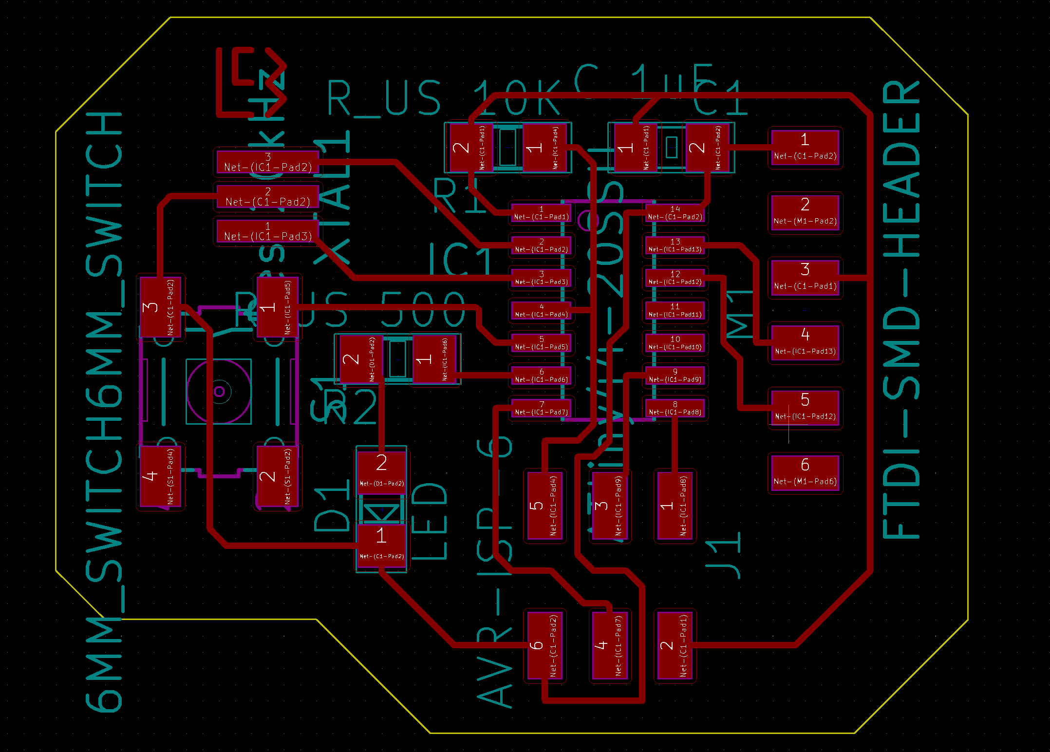
I saved the netlist and brought it into the KiCAD Board Editor. The rat's nest was pretty confusing to pull into the right places -- I used the original board layout for the unmodified echo board as a reference, which helped a lot. The grid was a bit finicky for laying out the traces, but I found that placing the lines down piece by piece could help, and a higher resolution grid reduced the excessive snapping. Marking the edges of the board was easy, at least.
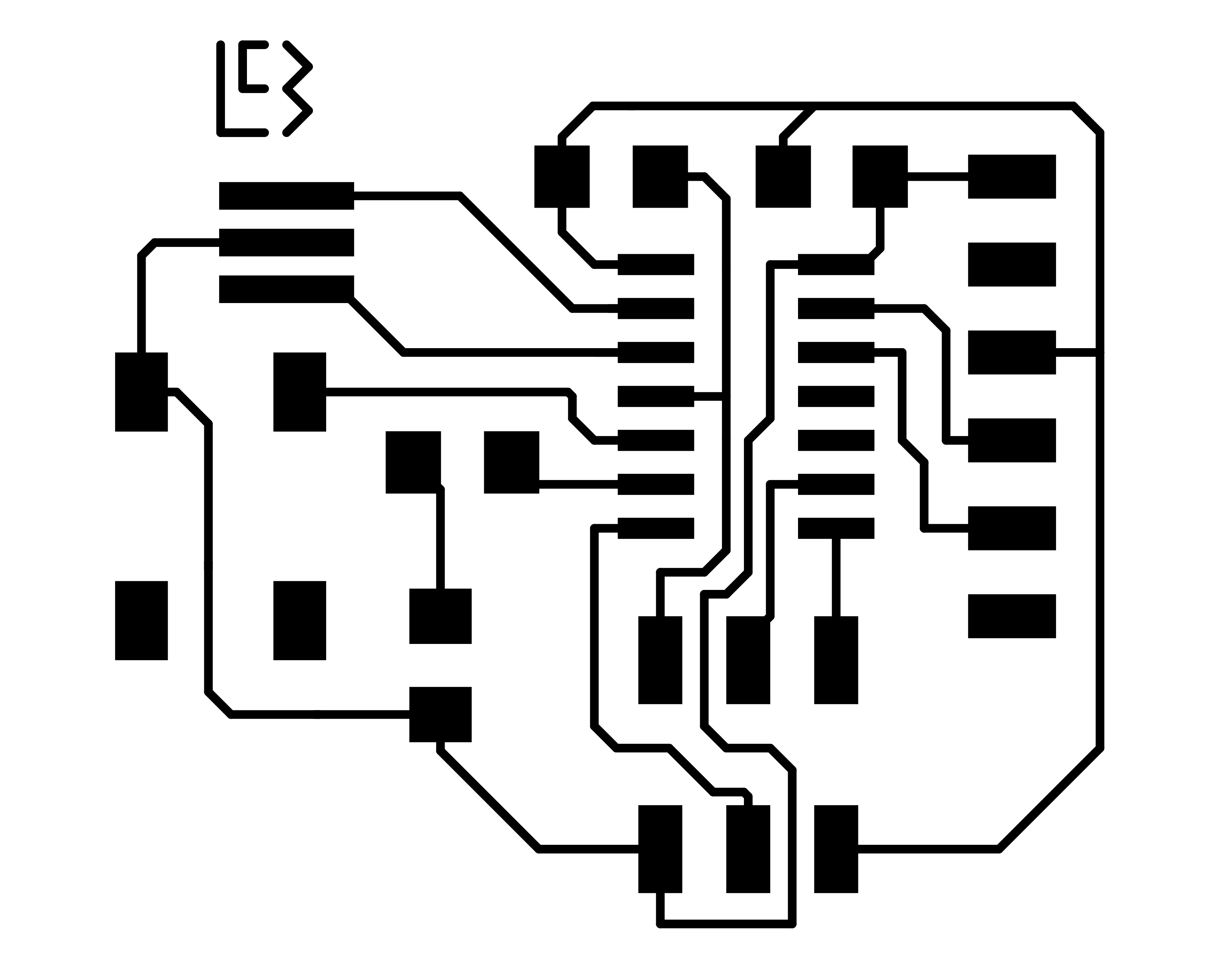
After exporting the traces to SVG files, I struggled a bit with inkscape to get them to load into mods properly. For one, I had some incorrect exporting options set, which pulled in the whole page I was working on. After that, I had a bit of trouble filling in the background as white so mods could invert it, and a bit of trouble with mods recognizing the edges of the board that were too close to the PNG edge. I solved the first by moving the traces into a layer on top of a rectangle in the background, and the second by widening the edge lines and keeping the image un-inverted.

The milling worked pretty well for the most part, but I noticed that some of my clearances were just barely too low, resulting in some connected corners that should have been separate. I took a knife to the ones I saw.
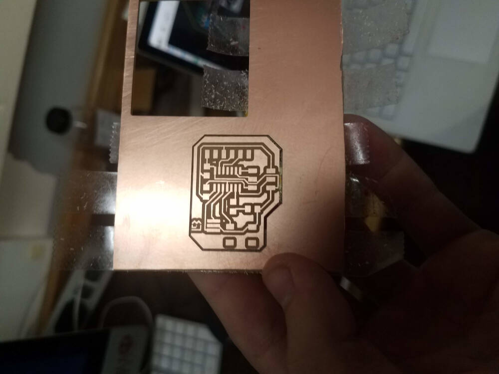
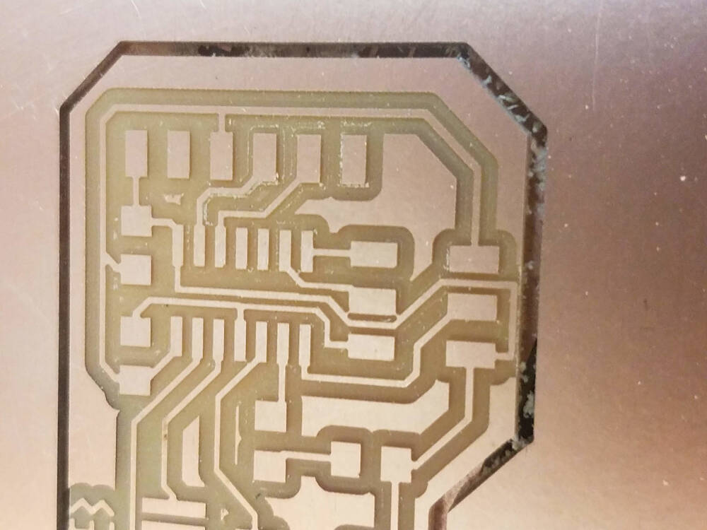
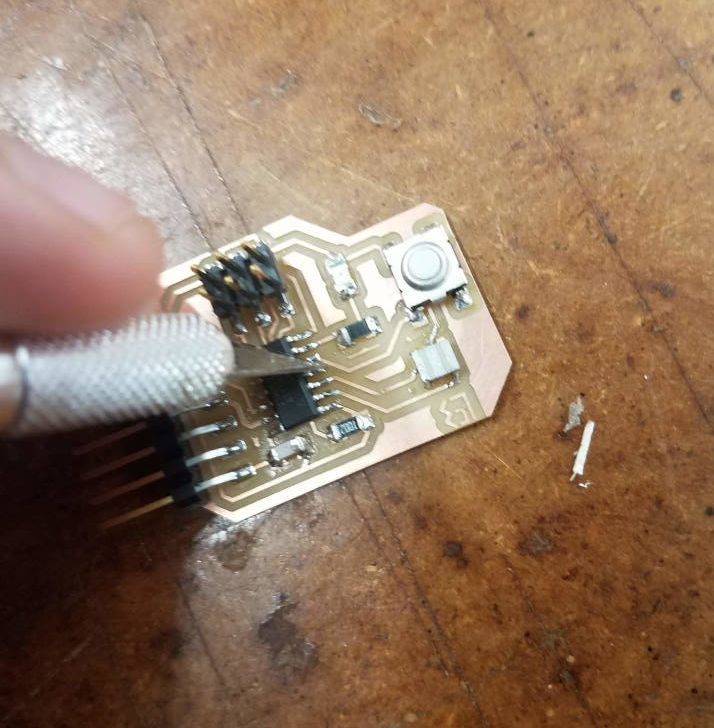
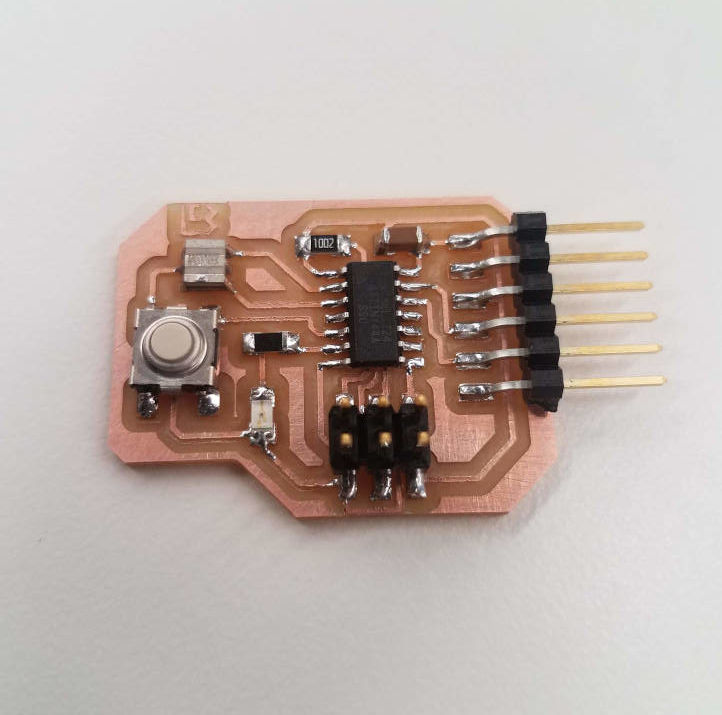
After laying out the pieces, I soldered all of them on, and some larger problems came up. Some of the corner connections hadn't been fully cut, so I worked through those with a knife. The multimeter was acting up, which I later figured out was an issue with being in AC mode while I was trying to use it for diode/connection testing, but it confused me at the time. Finally, if you paid attention to the earlier traces layout, you might have noticed (as I belatedly did) that the button orientation was off. I had made a mistake matching the correct footprint to an inaccurate symbol, which had set the button up just as a short connector as I had it. I couldn't get the rotated button to fit on the pads I had milled, and, with all these things combined, I thought it would be best to just try again.
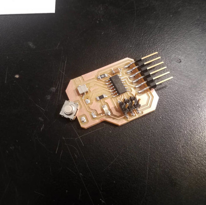
I updated the schematic, and was dreading having to re-route all the traces. Thankfully, KiCAD was super nice, and updating the netlist only added things to the board editor that I had added since before. This meant I could easily switch out the bad button layout with the good one. I gave the traces a little more clearance, and the board milled much better.
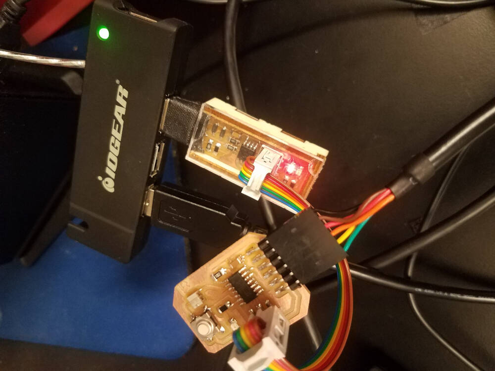
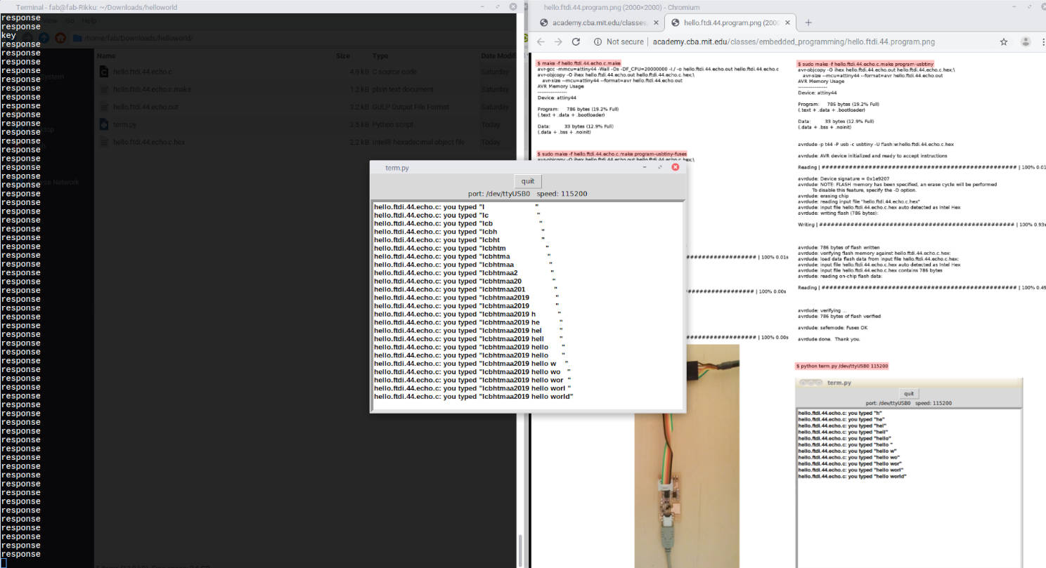
I tested more frequently as I went this time, and ran into no issues (especially after figuring out my AC/DC error with the multimeter). The soldering went great, and I programmed the board with my programmer from week 2, which felt suuuuper cool. After one unplug-replug, it all worked perfectly! I figured out that the board is storing 24 characters to repeat, but I couldn't get it to reset, so I think a fun use for the button and LED might be a reset switch -- holding the button down for x seconds turns the LED on and resets the stored string. I'll work on that in week 6!
I put some thought into the board setup for my final project, but I don't know enough about how the ATiny works with voltages and detection, so I left it as a rough workbook sketch for now. I'll document that along with the electronics programming for week 6.