SCROLL
finalProject 0000 0001 CAD 0010 cutting 0011 programmer 0100 3Dprinting 0101 elecDesign 0110 makeBig 0111 embedProg 1000 moldCast 1001 inputs 1010 outputs 1011 networks 1100 machine 1101 interface 1110 wildcard 1111 notes0101
Electronics Design
Sir, it’s shaped like itself and is as wide as it has width. It is only as high as it is and moves with its own legs. It lives on what nourishes it, and when the four elements leave it, its soul moves into another body.
Downloaded Eagle
Downloaded Fab parts library
Added it to Eagle > libraries on my Mac
Started adding components to my schematic
Neil's Components (in Eagle_Fav library):
- attiny44-ssu
- resonator
- res-us1206fab
- cap-unpolarizedfab
- avrispsmd
- ftdi-smd-header
My Additions
- 6mm_switch
- led
Here is Neil's example board:
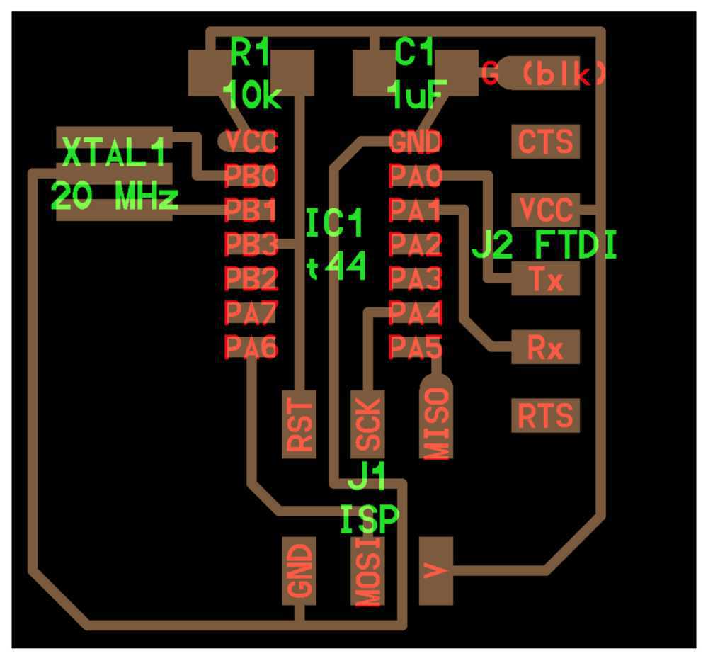
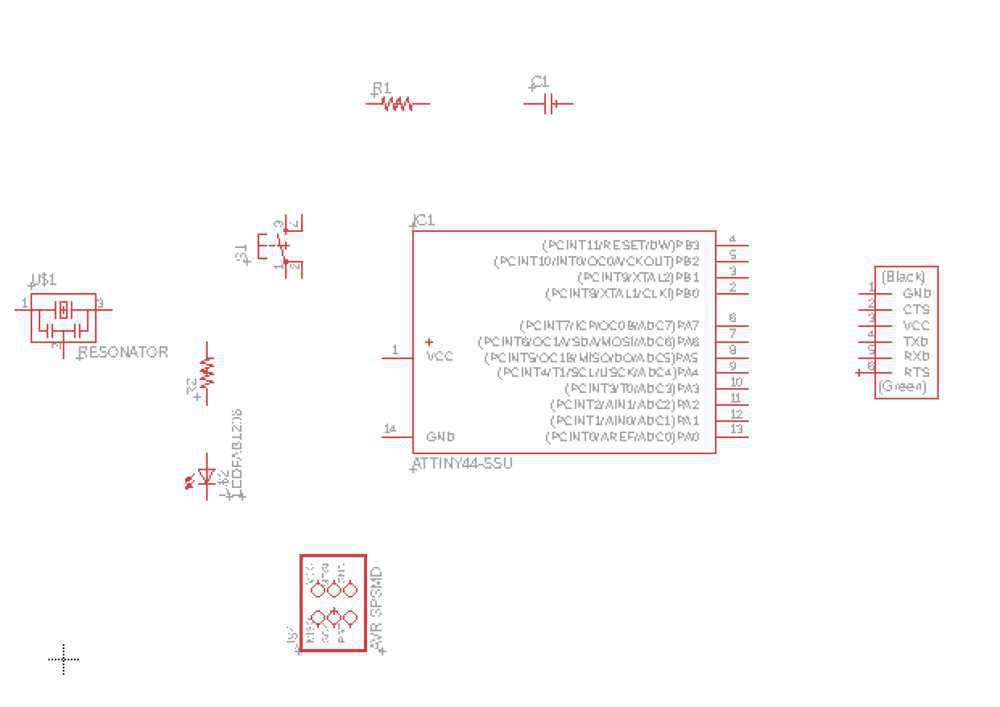
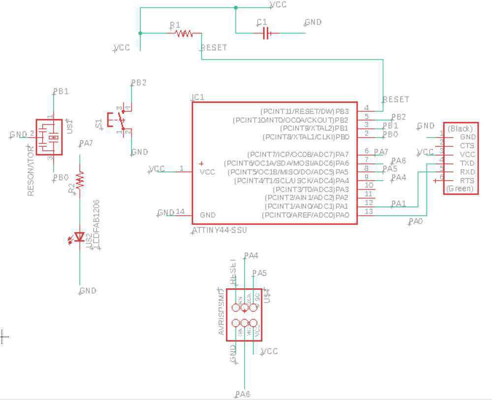
Schematic Attempt 1
A couple of nets (green lines) in this schematic are incorrectly drawn, but I don't find that out until later...
I am spreading all my parts out.
I figure that many people have already found a good way to organise these parts. I'm going to go through some students' pages from prior years.
Julia's page turned out to be a good guide.
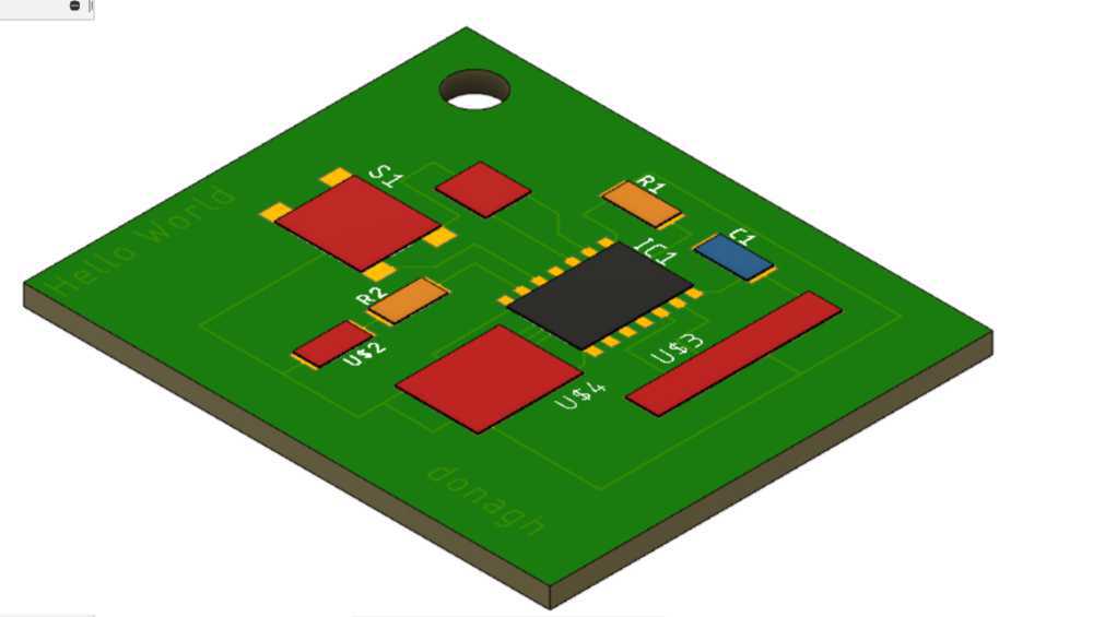
Here is my component layout following her example.

Going to try the auto route function first, just out of curiosity.
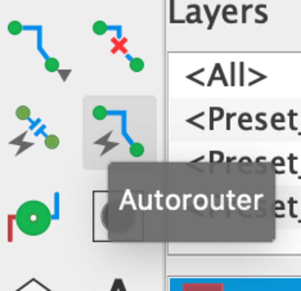
Unfortunately the auto-router reverted my board to a prior (ugly) configuration.
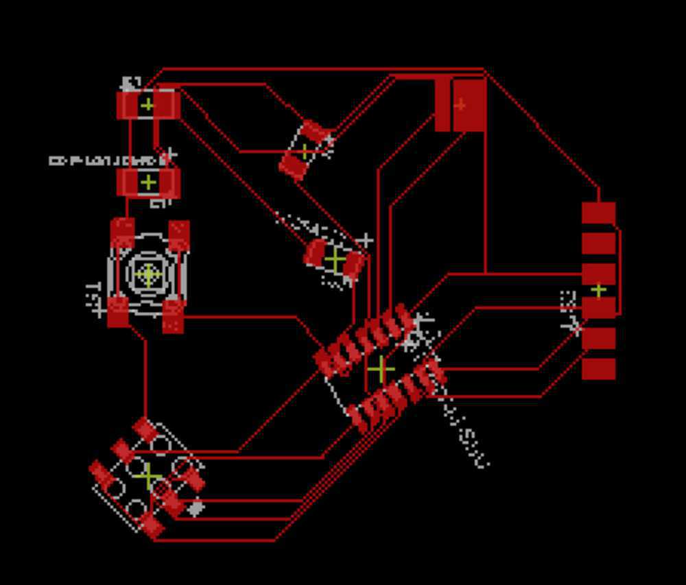
Back to the board drawing drawing board...
Good thing I documented my layout, because it won't let me command + z back to it.
Ok back in position, going to route by hand.
Just realised I have some of my schematics connected incorrectly. I could fix the two or three incorrect connections... or I could completely restart from scratch in order to drive home exactly how all this is supposed to be wired. I'm going to restart.
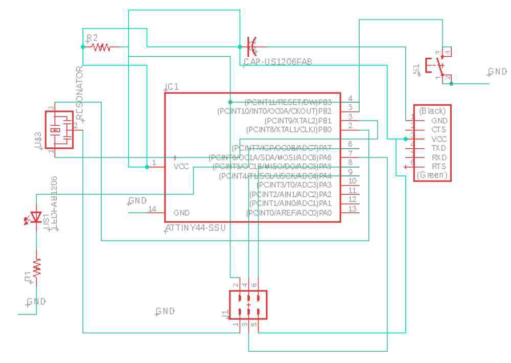
Attempt 2
Added in all the necessary components following Julia's layout.
Time to connect. I'm going to go top to bottom and try to understand the role of each component and why it connects to where it should. Disclaimer, I will describe what I think to be the case. Do not trust what I say, because I have no idea. If I'm misunderstanding something please get in contact with me and teach me!
I'm not going to draw the green lines to everything this time. Instead, I'm going to name each connection with it's proper terminus. I hope this will make it easier to understand.
CAPACITOR - this is here as a filter. It will reduce the 'noise' of the circuit by curtailing fluctuations in voltage. You can think of it like a ballon of air (thanks Rob!) that will expand to suck up the extra air in the system and shoot some air out to bring the amount of air up to the threshold. If the voltage rises above a threshhold (what defines that threshhold??) the capacitor will act as a sink for voltage. If the voltage drops the capacitor will release energy(?) to increase voltage.
One side connects to Voltage at the common collector (VCC). This is the power source.
One side connects to Ground (GND) because GND the voltage reference point.
RESISTOR (with capacitor) - I'm very unsure of the reason for this particular component. From what I can gather, without the resistor the charge would zap straight through the capacitor to GND. The resistor slows down the incoming charge which allows it to be stored in the capacitor.
- Branches off the wire from VCC (power) to the capacitor
- The other side connects to the RESET pin on the micro-controller.
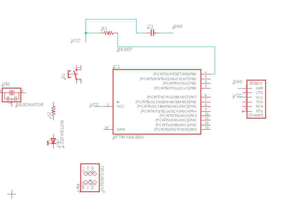
RESET - explain
- Reset on the micro-controller and reset on the ISP Header need to be connected
BUTTON - has four legs, but only two need be connected in our case.
- One side to a micro-controller pin (PB2)
- The other to GND
In series LED and RESISTOR
- Resistor is there before the LED so that the LED doesn't melt (why would that happen?)
- The series should begin from a pin on the micro-controller (PA7)
- And go to GND
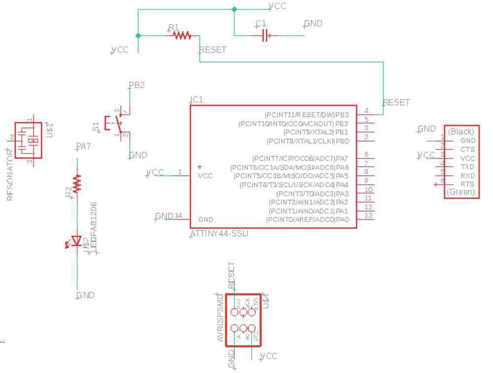
RESONATOR - explain
- 2 pin goes to GND
- 3 pin goes to PB1 pin on micro-controller
- 1 pin goes to PB0 on micro-controller (why?)
ISP HEADER - explain
- GND to GND
- RESET to RESET on microcontroller
- SCK to PA4
- MOSI to PA6
- VCC to VCC
- MISO to PA5
FTDI - explain
- GND to GND
VCC to VCC
- TXD to PA0
RXD to PA1
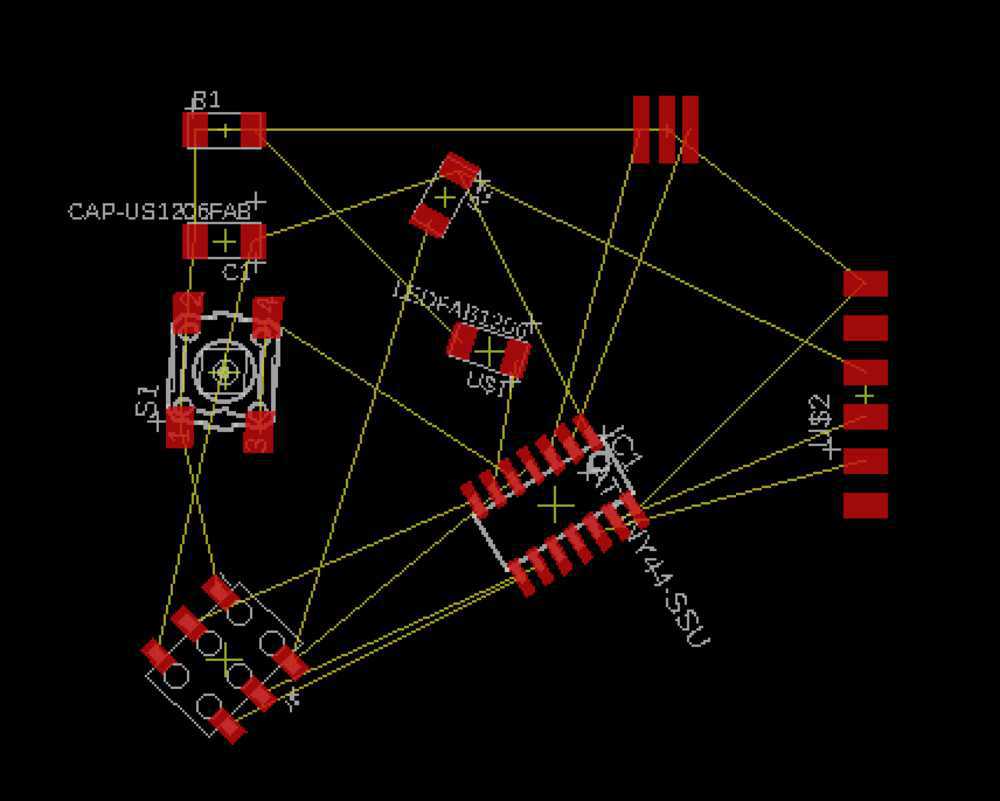
Routing
Switch to board view (button at top left of window)
I spread the parts out following Julia's example
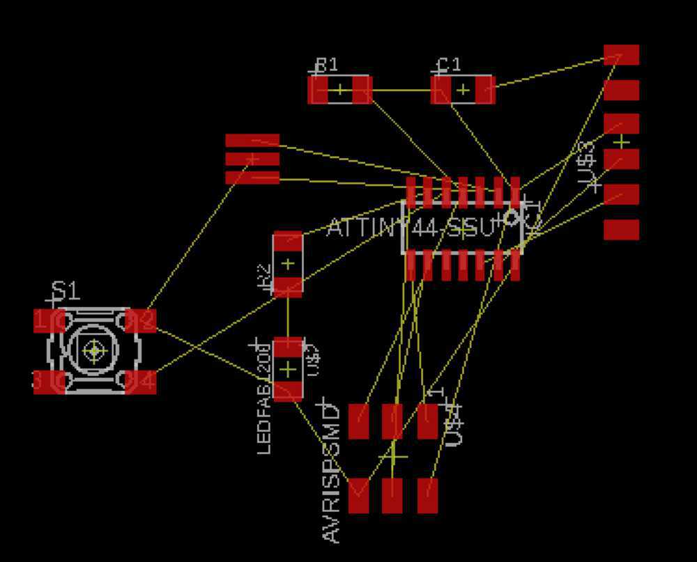
I hand routed the board using Neil's and Julia's designs as guides. Here is mine:
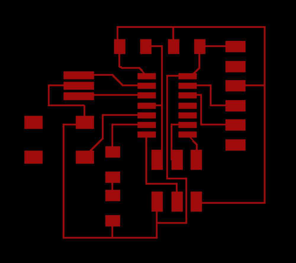
I was able to view the pads and traces without any other markings by toggling layers on and off in View > Layers.
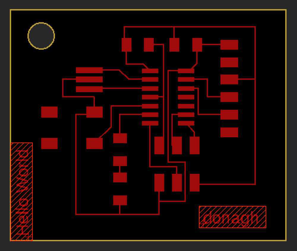
On the dimensions layer I am adding an outline, a hole for hanging and some ID text.
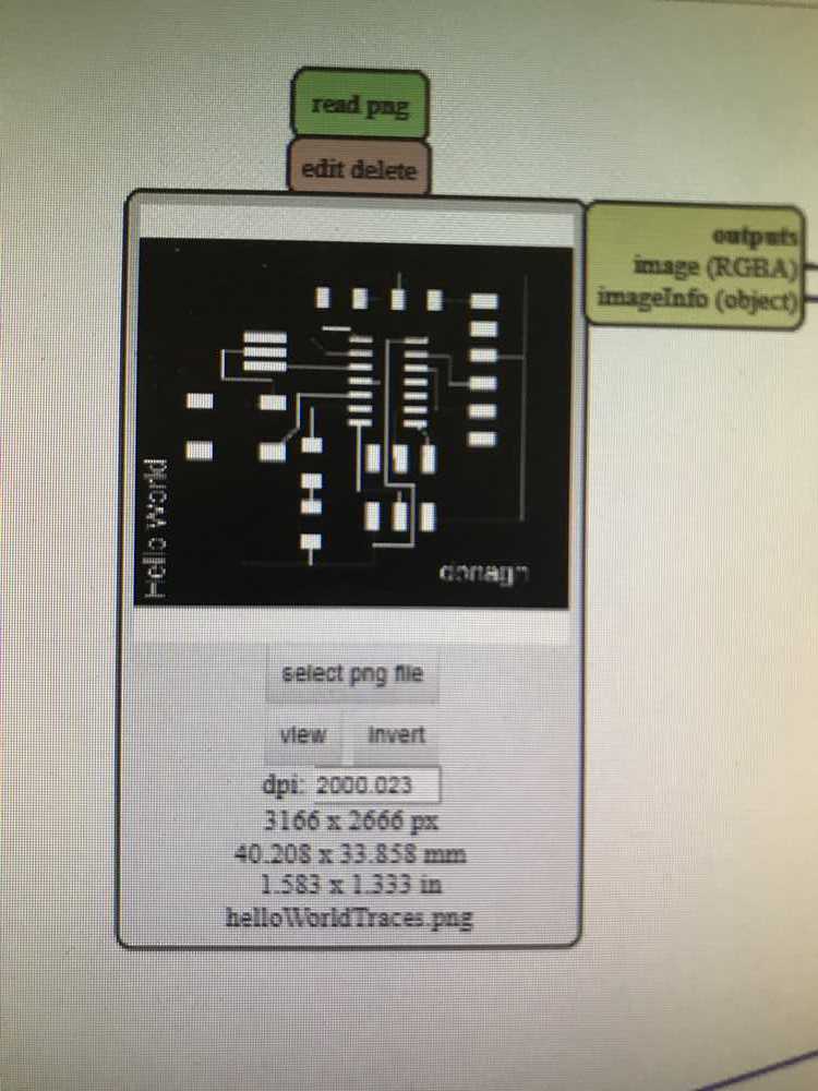
Time to export. I'm hiding all layers except for the top (where the traces are).
Then navigating to: File > Export > Image, making sure to tick the monochrome box.
I set the save location.
Made sure the image was exporting as a png
Set the dots per inch (dpi) to 1000
And clicked ok
Next in layer settings I made only the dimension layer visible.
And went through the same export process as the traces.
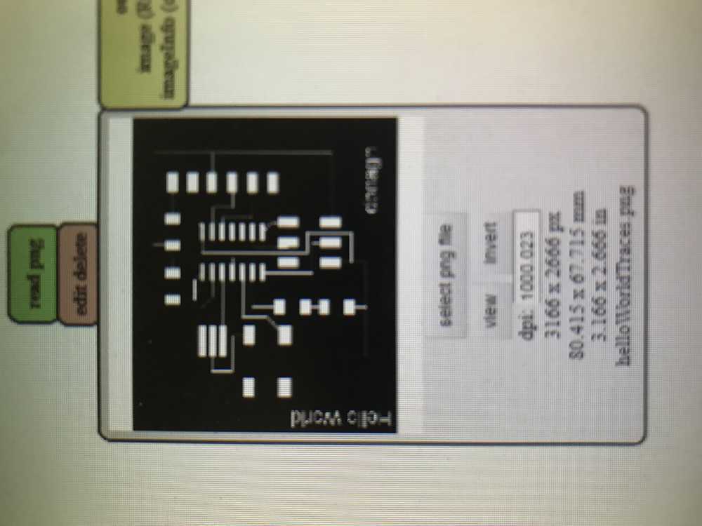
These were the resulting png files:


Milling
Uploading the png files to Google drive so that I can access them on the computer connected to the lab's milling machine.
Milling using the same process as I did for PCB programmer week
The origin for the first board is (90, 8, 0)
Running the machine
Stopped machine because 1) no white dust 2) the cut was way larger than it should be... looks like there was a discrepancy with the dpi settings in mods.
<img src"../../Downloads/iPhonePhotos/week5/individual/IMG_4132.JPG" width="500">
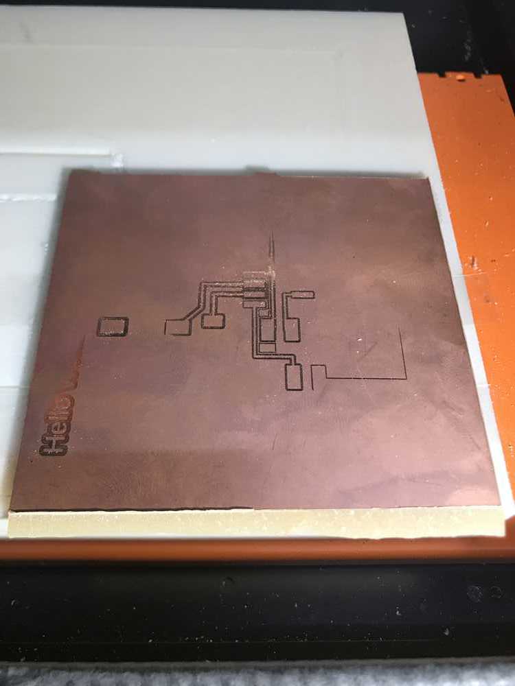
Rob told me that there is some bug in mods involving importing a png that was created on a Mac to the program. He said the dpi in mods, though it will read the same as the dpi of the image export, will actually be off by a factor of two. In order to correct this I multiplied the export dpi by two ( ) and put the new value into mods.
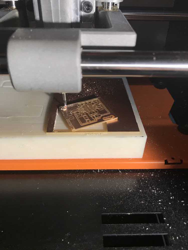
Rerun at the mill with a newborn and these new settings. I am seeing white dust now and the traces footprint is definitely more like what it should be. The board is flexing a bit every time the mill bit lowers onto it. I reckon our sacrificial layer needs a good milling over to level it again after the abuse we've been putting it through.
Had a mishap... The tape holding the board down was sliced all the way through and must not have been stuck down well enough. Luckily I was there to stop the machine before it ruined my board.
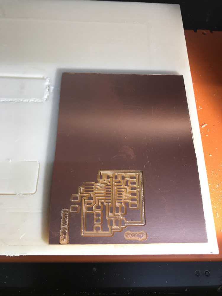
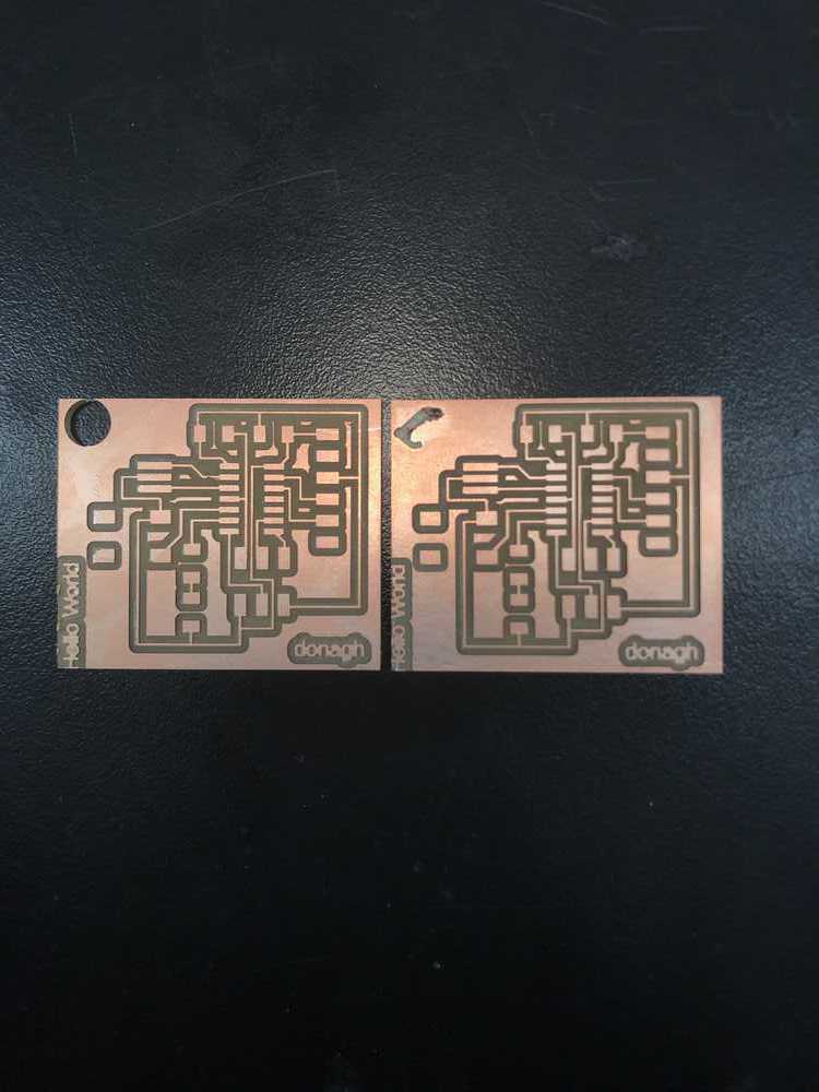
One board milled (and maimed)... The "Hello World" text didn't come out as I had hoped. It was too near the outline.
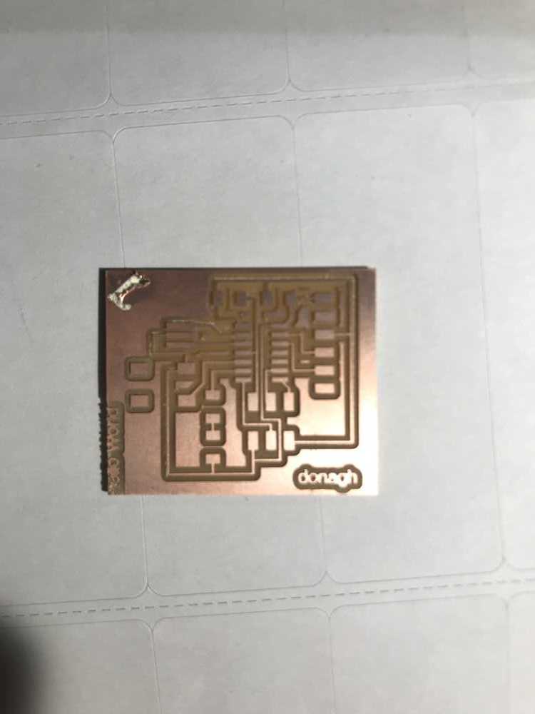
If I've learned anything in this course so far it's that I won't get things right on the first attempt. I'm going to make an extra board in case something goes wrong with the first.
I'm moving the origin back 1mm on the x axis in the hopes that the top of the "Hello World" text is not obliterated.
Soldering
To help orient my components on the newly milled PCB I pushed the design file from Eagle to Fusion360
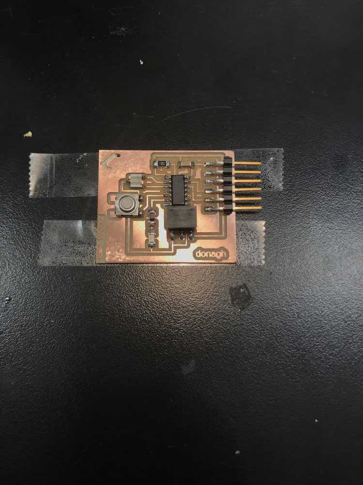
Using the same tools, procedures and lessons learned in (PCB Programmer)[] week, I prepared my board and began soldering.
Components:
- attiny44-ssu
- resonator
- res-us1206fab
- cap-unpolarizedfab
- avrispsmd
- ftdi-smd-header
Additions
- 6mm_switch6mm_switch
- red LED
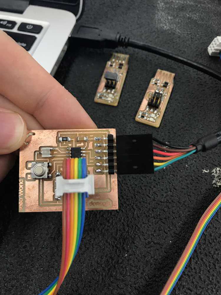
Finished Soldering
Programming
Julia's page is again proving invaluable.
I am downloading the C file and Makefile to my laptop from the course website. When I say downloading, I am copying and pasting the contents of these files into new files I made in Sublime. I then saved them under their respective names on my desktop. I have since realized that I could have just right clicked and saved as.
I am plugging my programmer from a couple weeks ago in to one of my mac's USB ports and using a FTDI to USB cable I am connecting my new board to another USB port.
Then using a header cable to connect my board and programmer, making sure that the wires are connecting the same pins on each (eg ground to ground)
Using ioreg -p IOUSB -w0 | sed 's/[^o]*o //; s/@.*$//' | grep -v '^Root.*' to list connected USB devices I can see
New board shows up as TTL232R
I am running make -f hello.ftdi.44.echo.c.make in the directory with the c file and Makefile I downloaded.
This created a .hex file in the same directory
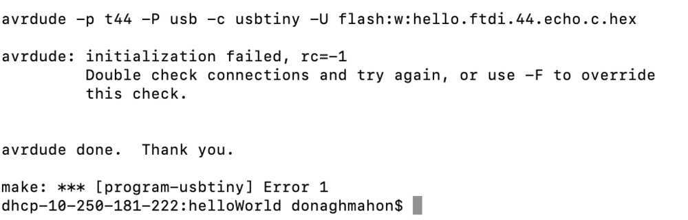
Now to send this file to my board:
Running: 'make -f hello.ftdi.44.echo.c.make program-usbtiny'
I got this error:
Playing around with the connections and then rerunning the command.
Eventually got this:
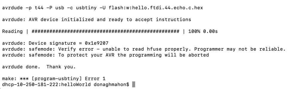
Googling around to find a solution and/or the cause of the error.
In different forums I am seeing references to "clocking" a board. I have twice seen a suggestion to add -u to the command to bypass the fuse checks, but judging by the terminal output it looks like a -U was added to the command in the make file.
I am checking the make file and indeed many lines include the -U, granted a capital U is not the same as a lowercase u. Odds are that it is something I have done wrong rather than an issue with the files.
I just keep running the make command in the hopes that something magically happens.
I did get a new error this time:
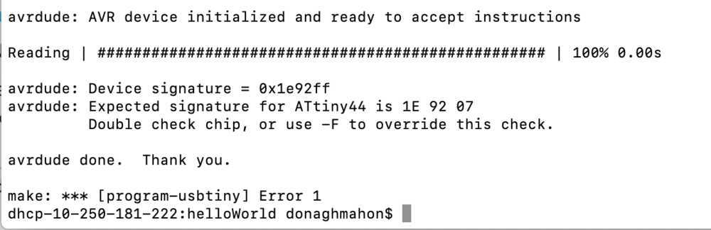
Tried my old switching the USB ports trick.
The make command seemed to have done something as I just got this output:
I ran the make -f hello.ftdi.44.echo.c.make program-usbtiny-fuses command and got the "Verify Error" again...
I think I need to call it a night and ask Rob about this tomorrow.
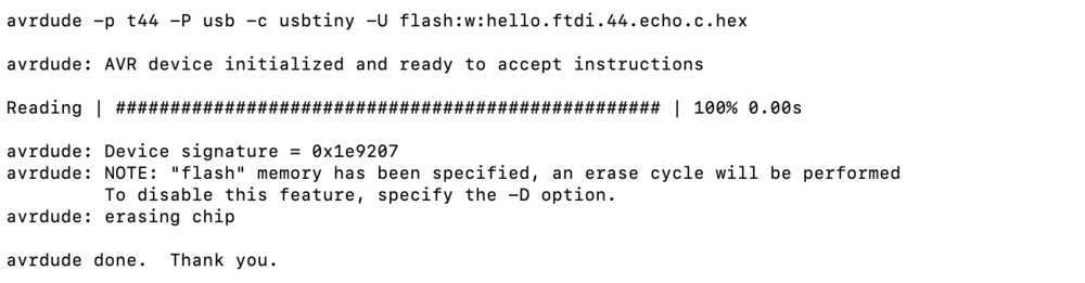
It's Monday morning and I'm back in the lab. I asked Rob for his assistance and he immediately points out that my FTDI connector is on backwards (the black wire is ground and so should be connected to my ground pin)... duh. I adjusted the connection to the below.
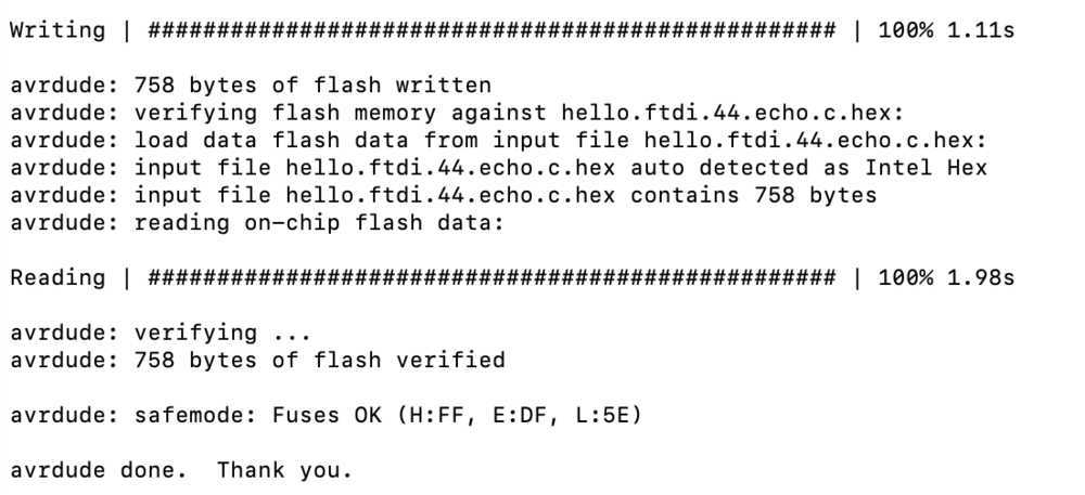
Running: make -f hello.ftdi.44.echo.c.make program-usbtiny
This is the output:
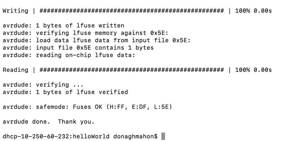
Running: make -f hello.ftdi.44.echo.c.make program-usbtiny-fuses
Output:
Disconnecting the programmer
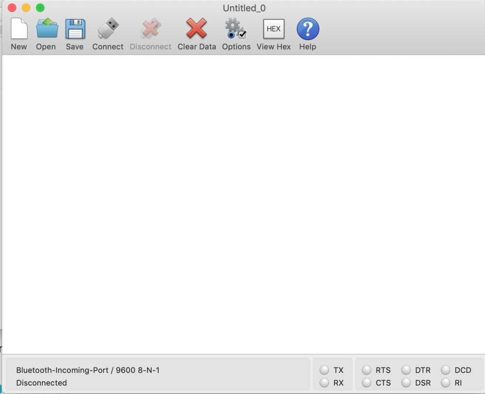
As per Rob's suggestion I am downloading coolTerm to communicate with my Hello World board.
CoolTerm window looks like this:
I navigated to the options menu and set the following
Bitrate to 115200
Port to usbserial-FTADUGMM (my board)
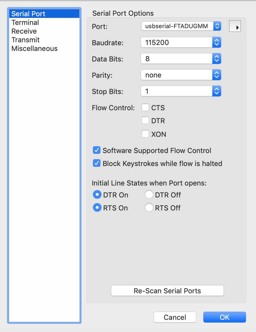
I clicked 'Ok'
Then 'Connect' on the top menu
The bottom menu then read:

At this point I just started typing characters and the board returned them to me!
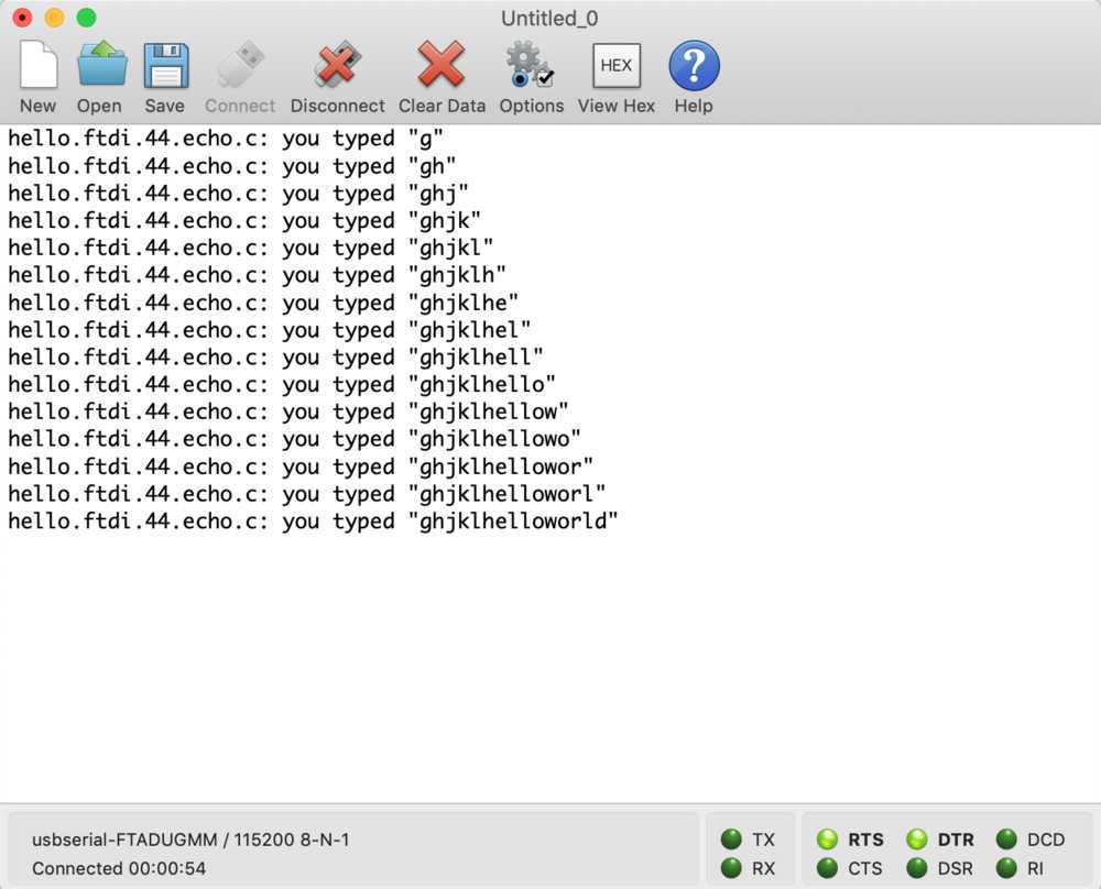
Success!