SCROLL
finalProject 0000 0001 CAD 0010 cutting 0011 programmer 0100 3Dprinting 0101 elecDesign 0110 makeBig 0111 embedProg 1000 moldCast 1001 inputs 1010 outputs 1011 networks 1100 machine 1101 interface 1110 wildcard 1111 notes0011
PCB Programmer
Group assignment:characterize the design rules for your PCB production process.
Individual assignment:make an in-circuit programmer by milling the PCB, program it, then optionally try other PCB processes.
Group Assignment
Characterise the design rules for your PCB production process.
Individual Assignment
Make an in-circuit programmer
References:
I used Brian's page as a reference for the following processes.
Characterising the milling machine
I downloaded the traces test file from the course website and loaded the png into Mods. I wanted to test cutting the png with both the 1/32 inch and 1/64 inch bits, even though I was pretty sure the 1/32 inch bit wouldn't be able to cut the majority of this file properly due to being too broad.
First I cut the file using the 1/64" bit. With the following Mods settings
I then simply switched to the 1/32" mill bit without changing any settings (other than the cut origin).
This is what I got:
As you can see the the 1/64" bit successfully outlined all of the lower, protruding traces. No such luck with the upper medians. The bisecting troughs were only cut in the last 5 blocks (0.16 and up). This shows that throughs thinner than 0.16 cannot be cut by the 1/64" bit.
As for the 1/32" test, some serious things went wrong. Firstly, there was a huge stretch of copper in the middle that was left untouched, despite either side being cut. My best guess is that this is due to the fact that I left the 1/64" settings entered in mods in place. Amongst other things, this would cause the machine to attempt milling traces the bit was too wide for. The untouched strip of copper in the middle could be the result of the incorrect tool depth setting (meant for the 1/64" bit), a bump under the PCB or a loose mill bit.
I chaged the tool width in the 1/64" setting to match the width of the 1/32" bit(0.0312), keeping the rest the same and ran a third cut.
This was the result:
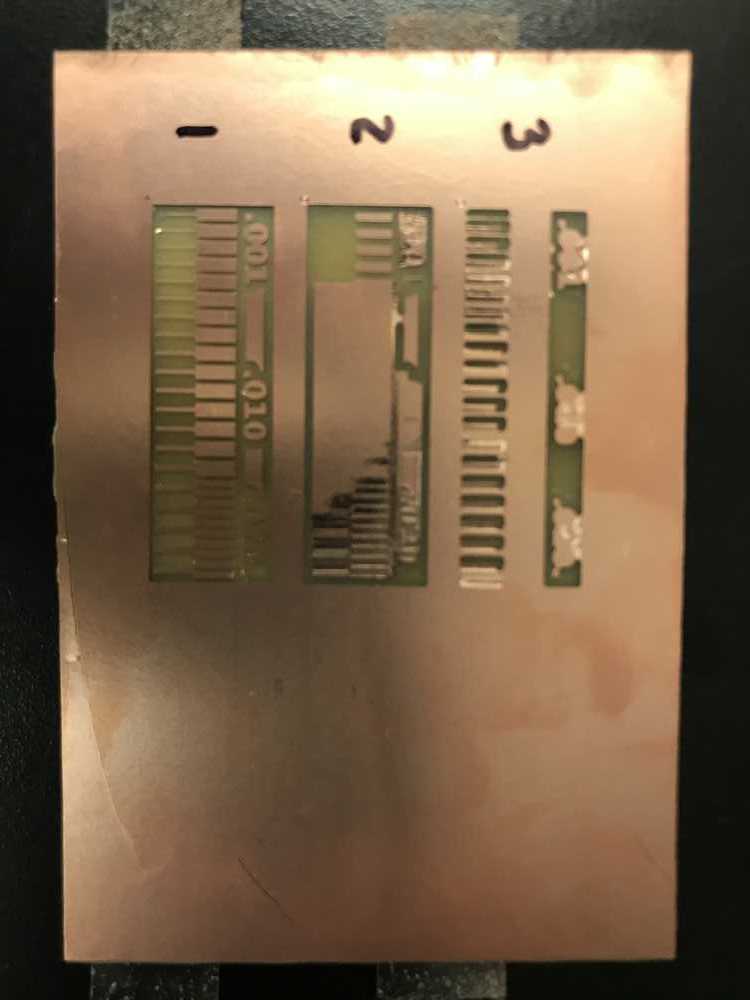
Conclusion:use the 1/32" bit for cutting all the way through the PCB or for striping large areas of copper. Use the 1/64" bit for circuit traces.
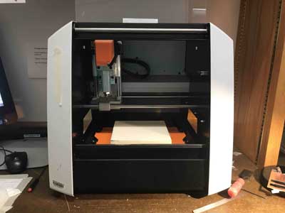
Milling
Steps:
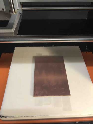
Cleaned off the "sacrificial layer" (white block) in the Roland milling with a blunt chisel. I'm doing this to prevent tiny lumps of left over material underneath my PCB tilting it, throwing off the cut.
Applied strips of double sided sticky tape (non-overlapping, so as not to tilt the board) to the back of the PCB.
Stuck the PCB down inside the milling machine
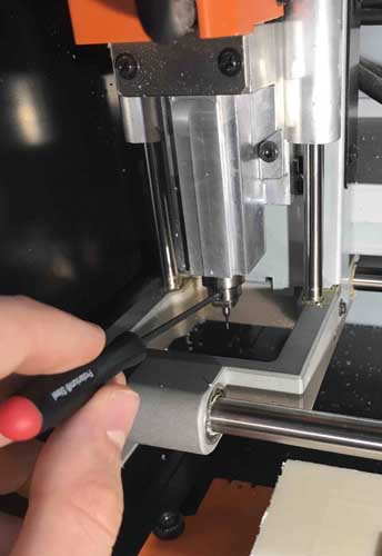
Examined the machinery to check for anything out of order. Specifically, paid attention to the mill bit currently inserted. I am going to cut the tracks of the circuit first and then cut the deeper outline after. This is important as cutting the board out of your larger piece of PCB first will increase the liklihood of your substrate moving around during milling.
The 1/32 milling bit was inserted in the machine, but I needed the finer 1/64 bit to mill the tracks. Time to switch the bits.
With my left hand I reached under guide rails and held the bit to be removed. This is important as when the securing screw is loosened, the bit is realease from the mill and, thanks to gravity, falls out. These bits are not only fine but extremely brittle, hence, shatter easily.
With my right hand I unscrewed the screw holding the bit in the machine. It only took a half revolution as the screw is only meant to be tightened to "snug", not as tight as possible.
Due to the awkward wrist contortion necessary for reaching under the guide rails and up to the mill bit - it is necessary to reach under, rather than over, the rails as the bit needs to be lowered out of the chuck (the part that holds the bit in the machine) after it is released - I was holding the bit like a cigarette between two fingers, underestimating the weight of the bit. When I unscrewed the chuck screw, the bit fell straight through my fingers and landed in the bed of the mill with a clatter. Luckily it did not break. Lesson learned.
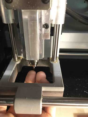
I held the 1/64 bit in the chuck and retightened the screw until just snug.
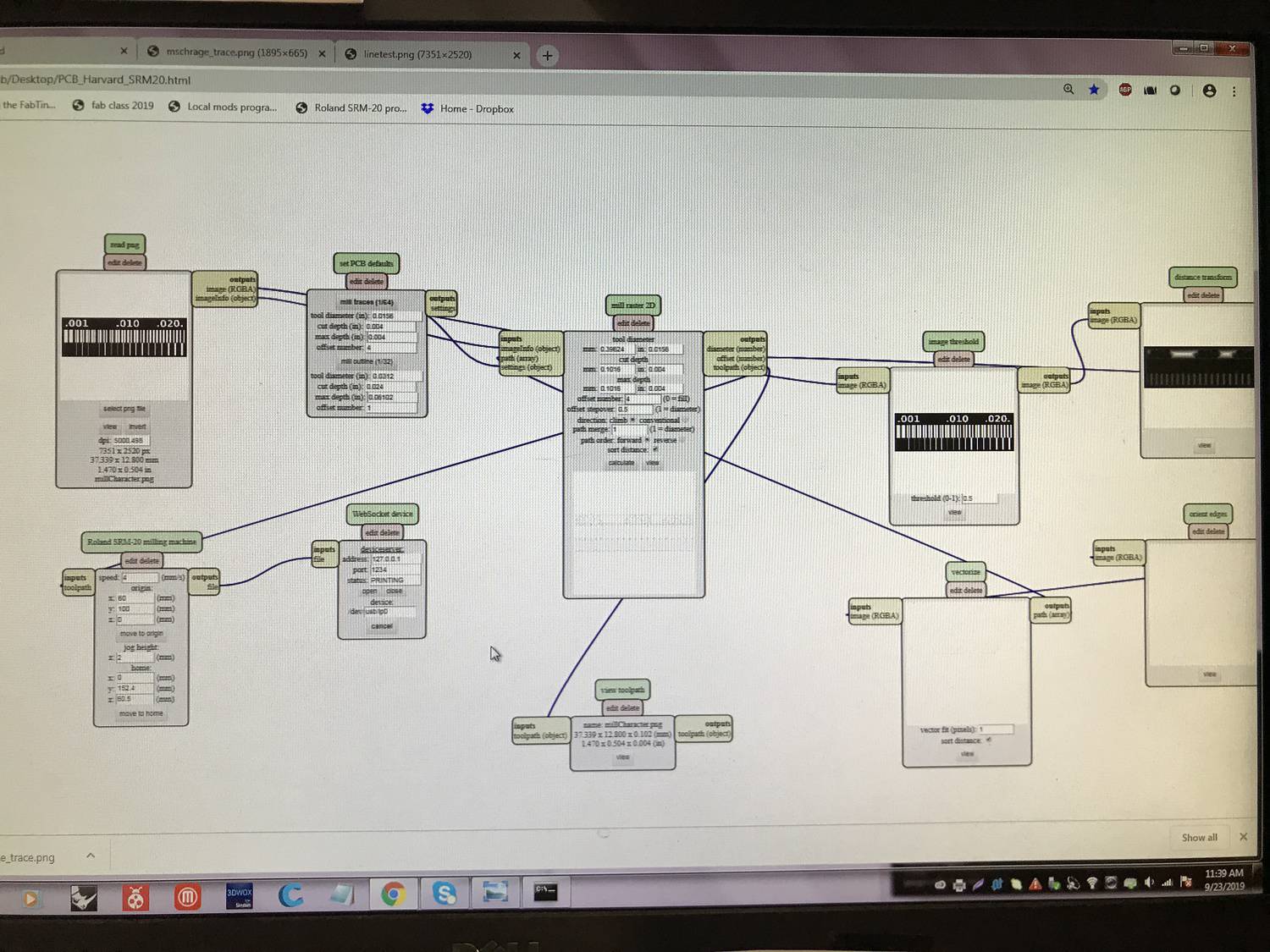
I started up mods on the nearby desktop and uploaded the traces png from Brian's page.
I set the origin to a desirable location (77, 35, 0) - I am record the origin point so that what I go to cut the outline I can set the bit to start in the same place so the properly line up the outline around the traces.
Holding the bit, I unscrewed the holding screw and slowly dropped the bit down until it rested on the copper.
Holding the bit down, I retightened the screw to snug.
Pressed calculate and then send to printer. The mill did its thing.
When the job was complete, I waited 5 seconds before opening the machine door. Opening withing 5 seconds causes the machine to go into a mode which prevents operation. The mill would then have to be turned off and back on again to continue working.
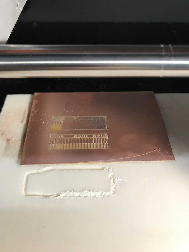
I vacuumed out the debris and examined the job
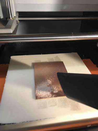
Judging by the spindles of copper spirling off the board, the 1/64 bit may be too sharp for its own good. A more worn bit will give a clean cut without the spindles.
I closed the door to the machine, changed the origin to (77, 65, 0) and repeated the process for a second and then third (77, 90, 0) board. I had a feeling I would need some extras in case something went horribly wrong during soldering.
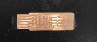
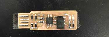
Here is the PCB after the last cut
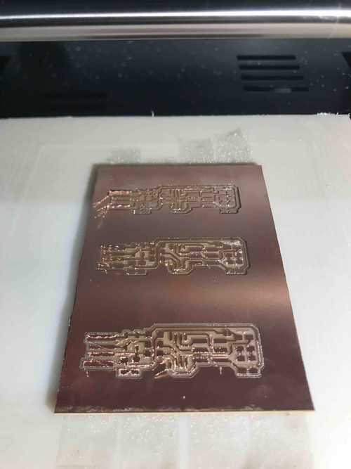
Time to cut the outlines.
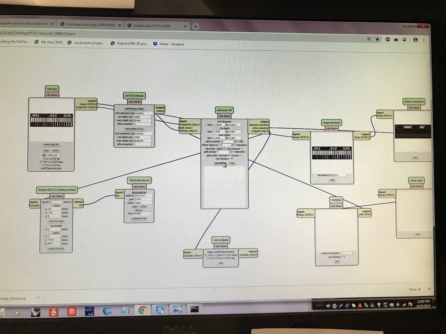
Loaded up the outline png from Brian's page into mods
Left the origin the same as my last cut - working in the reverse order this time.
Pressed calculate
Just after I started the machine I realised I had forgotten to change to the 1/32 inch bit, which will do the deep cutting job better. I emergency stopped the machine and changed the bit the same way I had earlier.
In the 'set PCB defaults' module in mods I switched to the lower setting buddle labelled "mill outline (1/32)
Recalculated and sent to printer.
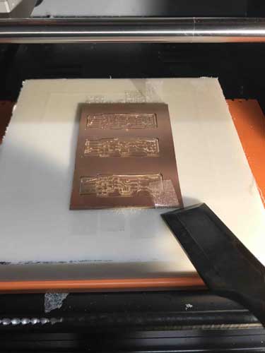
After each outline was cut, I vacuumed up the debris and changed the origin to origin that was used to cut the traces of the next board.
Here is the PCB after all the cutting and the blunt chisel I used to carefully remove the PCB from the sacrificial layer.
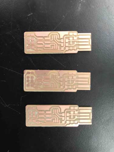
Here are the three boards:
Soldering
Steps:
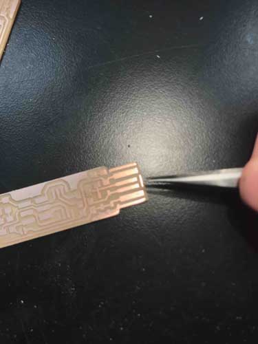
First I sanded the copper side of the PCB with 400 grit sand paper in order to remove the copper spindles and burrs.
Using sharp tweezers I scraped off the excess copper at the tip of the USB connectors
Washed the board with soap and water, then dried.
Rinsed the board with isopropanyl alcohol and dried again.
I forsaw that soldering these tiny parts would be a finicky affair and it would probably be helpful to limit the amount of moving pieces. I stuck a strip of double-sided sticky tape onto the work top and placed the board to be worked on on top.
I gathered the tools and materials (save for the components) I would need for the task.
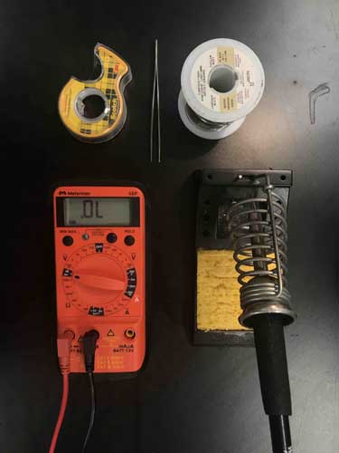
double-sided sticky tape, sharp tweezers, 0.5mm solder, multimeter, soldering iron
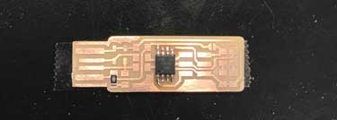
I places the microprocessor on the board first as it is easiest to work from the inside out to prevent having to reach around components in the way later in the process.
The best technique I found for soldering was:
place a dolop of molten solder on the iron
place the iron, dolop down, on the copper just away from the component leg to be soldered
introduce more solder to the copper area between the iron and the leg. It should flow over the leg and surrounding copper pad.
lift iron off
Here are some progress shots:
The components were trickier than expected to maniupulate. What was expecially frustrating was that as soon as the solder touches a loose component, the component would be pulled towards the iron and all the work I put in to place the component exactly where I wanted it was for nothing. I did get better at repositing the components as I was soldering with the end of my solder wire.
As I went on my joints were getting shiny and smoother. It was satisfying to see.
Eventually all the components were in.
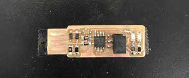
Following the suggestion on Brian's page I then covered the USB connection prongs with solder in order to build them up higher off the board to have a better chance of reaching the connector in a USB port
Brian's documentation suggest adding a thin plastic layer to the back to further thicken – I couldn’t find any plastic packing in the lab so I began cutting some canvas I found to add to the back – however quickly realized the fibrous constitution of the material was not ideal for sticking inside a computer – some fibers may fall off inside
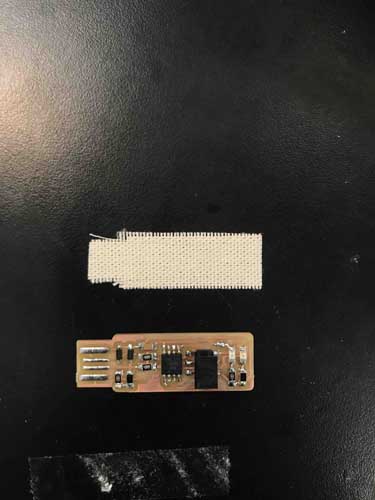
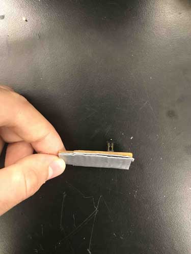
I found some duct tape and used that to build up some thickness on the underside of the board. It is a little too thick (and ugly). Next time I will stick only two layers directly onto the back of the PCB.
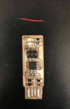
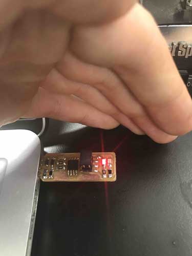
Into my laptop it goes!
Red LED shines, one victory in the bag.
Time to see if I can flash it using a working programmer
Turning this hunk of parts into a programmer
Following Brian's instructions, I am setting up the proper development environment on my mac.
Downloaded and installed CrossPack
Downloaded the firmware source code and extracted the zip file (See Brian's page for these steps and source code).
In terminal: cd into the fts file
ran 'make'
.hex file appeared
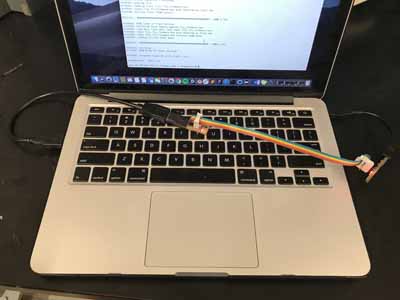
I connected programmer to my mac via usb extension cable
THE FOLLOWING IMAGE IS NOT HOW TO SUCCESSFULLY COMPLETE THIS STEP! However, it is what I thought I had to do.
This is where I ran into issues. BE WARNED BRAIN'S PAGE, while an amazing resource, one I would be lost without, SKIMPS ON THE FOLLOWING VITAL DETAILS!
Figured out by trial, error and a invaluable assist from Victoria, this is what I did to get the board programmed.
You must connect your unprogrammed board to one USB port in your computer
Connect the working programmer to another USB port in your computer
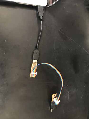
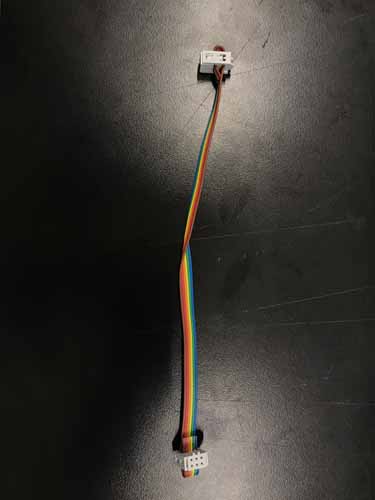
Connect the programmers to each other via a ISP cable like this one I made.
This IS how to configure these connections:
Make sure that the wires in the cable are connecting the ISP header prongs to their same respective progs in the other programmer.
You will know you have done this correcty when the red LEDs on both programmers light up BRIGHTLY. If they are glowing dimly, the connection is not in the correct orientation.
Next I ran 'make flash'
Several times terminal would give me "Error: Could not find USBtiny device"
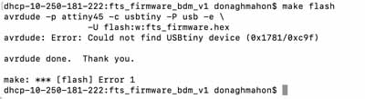
This caused quite a bit of frustration, but I eventually figured out that if everytime I got that error I switche the USB ports the programmers were plugged in to, I wouldn't get the error anymore. This most likely had less to do with the swapping and more to do with rigging the connections between all the boards and cables so that signals could flow again. I will say that while I know that is probably true, it was uncanny how the swap worked every single time whereas physically moving the cables around and pressing connections together without swaping ports never did.
This would have all been very nice to know from the get go, but instead I spent along time trouble shooting. This trouble shooting consisted of:
soldering up two more boards
trying to flash those unsuccessfully
checking all my componesnts using a multimeter (silver lining: I learned about continuity).
tested continuity between Vcc and GND – no beep like the page says would occur if there was continuity hower the multimeter is reading .519 ohms for my new board and 1.267 for my old board – the above page says anything over .3 ohms indicates continuity. The “working” programmer in the lab gives reading of .516 ---- seems like I should be good to go with the 0.519 ohm board. I later found out that the copper had almost completely worn away on part of the 1.267 ohm board. This could have been the cause of the high reading.
I discovered this terminal command for listing USB devices connected to your device: ioreg -p IOUSB -w0 | sed 's/[^o]*o //; s/@.*$//' | grep -v '^Root.*'
The most reliable USB connection came from adding USB connector housing to one of the boards
The second best connecting board had two layers of duct tape applied on top of eachother on the back of the PCB.
Eventually, all my boards were consistently being recognised by my laptop. I could then flash them and run 'make fuses' along with the subsequent commands outlined on Brian's page.
Using the USB listing command, the programmer shows up as USBtinySPI

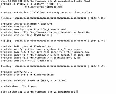
Successfully flashing looks like this:
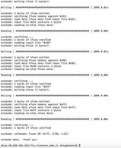
Successfully running 'make fuses' looks like this:
I went through the entire process with one board, used that to program the second then used that one to program the third.
When all were working, I repaired the board with the worn trace using some wire and solder.