PCB Design
Two weeks ago we fabricated a PCB board without knowing much about how the board itself works; This week we get to design a PCB ourselves.
Solving tricky problems at each step, I eventually managed to design and layout my board in KiCAD, milled it, stuffed it, figured out why the heck it did't work (with a lot of helpful help from Zach the TA), flashed a binary onto it, and wrote my own little program (a binary number calculator using the 1 button and 1 LED, scroll to the end for video demo!) via the Arduino IDE.
Due to my work in previous weeks, many people expected me to come up with a procedurally generated PCB. However, since I was completely unfamiliar with the medium and the design process, I was more anxious to produce something that works at all. Therefore, I went with the standard approach to produce a minimal and functional board first, and maybe save the fancy stuff for later when I'm more confident with the medium.
Schematics
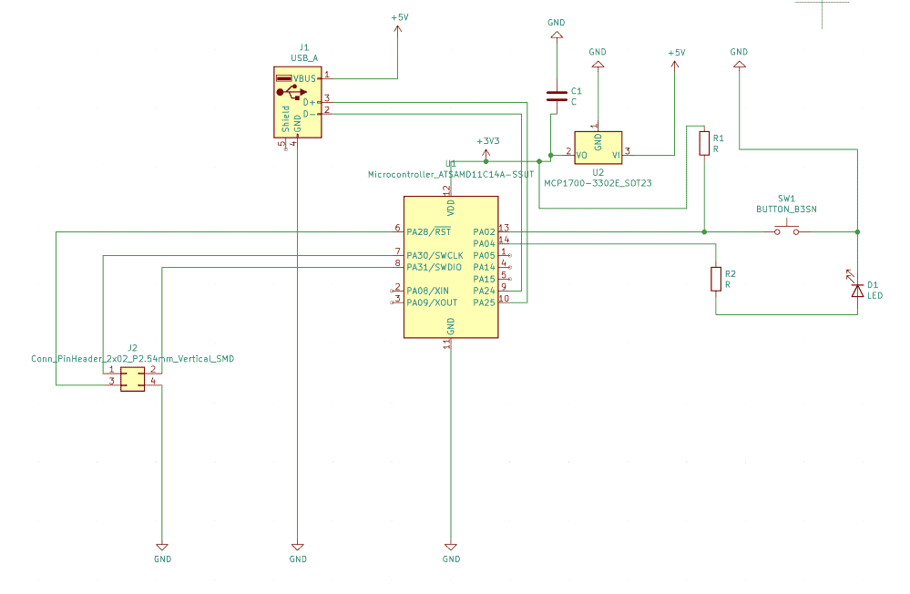
My first step was to look at Prof. Neil's reference board and guess what each part correspond to in KiCAD. Few of the names perfectly match; but I don't want to get stuck, so I decided to take my chance at guessing for the time being, and later check with the TA's.
Though I learned at recitation that we can use labels in place of some wires to reduce mess, I decided to stick to as few as elements as possible in case there're unknown catches, so I used wires all the way.
I added a button and a LED, as required by the assignment.

I thought my messy ball of yarn looked kinda cool. But when I showed it to Jake our TA, he pointed out the fact that it is completely unreadable. So following his advice, I cleaned it up by using “GND” and “5V” labels wherever the wires go those ways. Jake took a quick look again and spotted my error, which was that the wire after the pull-up resistor after the switch should go to 3.3V instead of 5V.
Layout
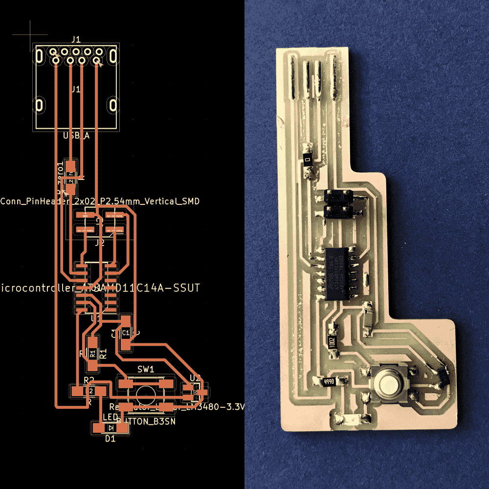
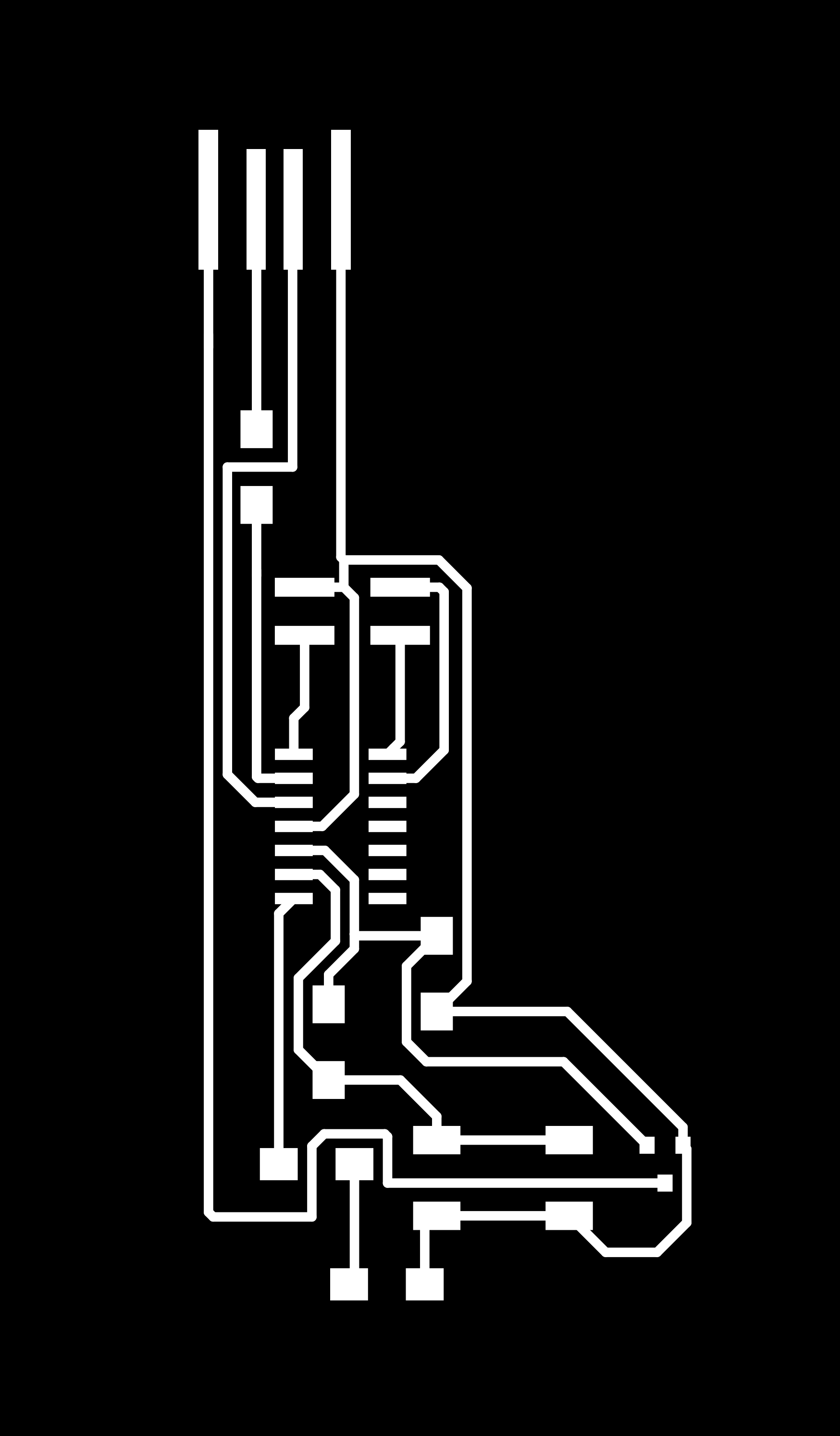
Before checking the schematics with Jake I was already working on the layout (you can see in the first schematic above there're two “useless” resistors which I used as jumps in the layout).
It was a very hard topology puzzle, to find a way to wire all the parts minimizing the number of jumps. But I enjoyed it a lot, in fact, I think it is more fun than many puzzles. My reasons are:
- For each distinct PCB schematic, laying it out is a new puzzle never before solved.
- Unlike many puzzles that have roughly two states, unsolved and solved (when you figure it out you totally figure it out; when you can't you really can't), solving PCB layout is rewarding all the way, like when you reduce 4 jumps to 3 jumps, 3 jumps to 2 jumps, etc. And you can call it a day whenever you feel happy with what approximate solution you currently have.
Three times, three times I started over with completely different layout, after feelings of hitting local optima…
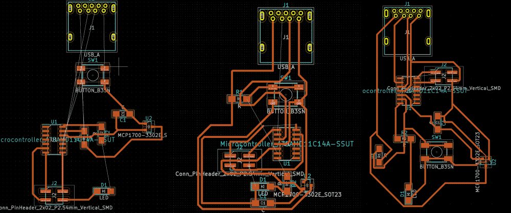
… before finally reaching my best design below, which only uses a single jump. In fact, that one jump might be inevitable given the order of the USB pins and those of the microcontroller -- but you never know, perhaps there exists a perfect design! Anyways, I was very proud of myself for the time being.
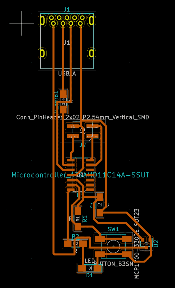
My guiding principle was this: A wire can go under many parts like capacitors, resistors, pinheads, etc. These are “free” jumps, move these parts to critical places so that the free jumps can be used as much as possible. If there's a part without a wire passing underneath, it's a waste!
About KiCAD: as an open source software, it is surprisingly usable. Everything makes sense and I never felt lost or confused. I like it a lot better than FreeCAD, blender, inkscape and gimp. (Or maybe it is because it is the only ECAD software I've ever used, so I don't know what “good” means). My only complaint is that when moving the parts, the wires just stay where they were. In layout mode perhaps it is difficult to program a smarter behavior, but in schematic view it shouldn't be. That said, being “dumb” is still much better than attempting to be “smart” and failing. Maybe I'll also give EAGLE a try next time for comparison.
Export
The next step was to export binary images of the traces and the outline, so they could be milled by the machine.
My board involves a USB connector, the footprint of which doesn't exist in KiCAD by default. So I came up with a simple hack: I took the PNG files of Neil's outline and traces, chopped off the USB part, and pasted it onto mine in photoshop. I took good care to make sure the image resolutions match, and the positions perfectly aligned.
(Later the USB footprint was uploaded by the TA's for the class, but I already finished fabricating the board)
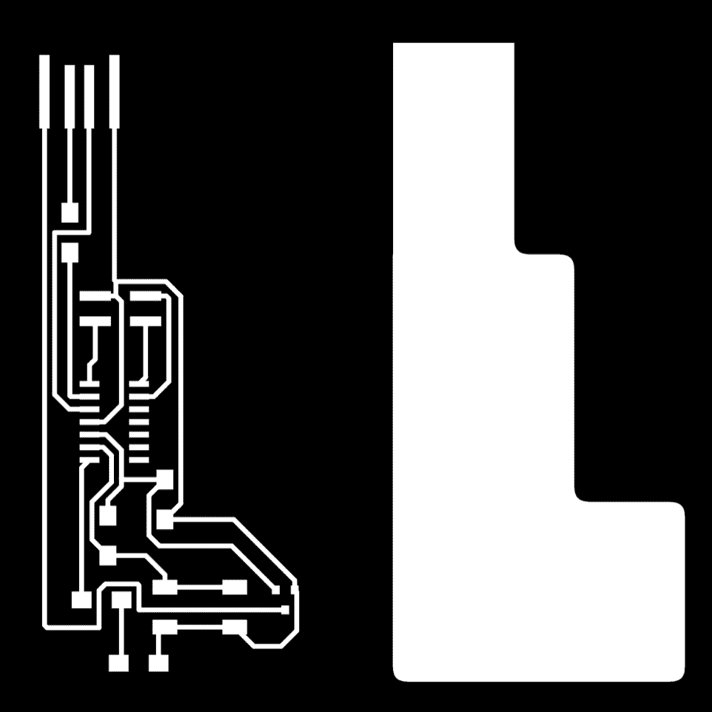
I drew the outline in photoshop too, since the shape drawing functionality seems to be a bit limiting in KiCAD. At one point I made the outline into the silhouette of a foot, but decided it was silly. I settled on a minimal shape that encapsulates the traces, with chamfered corners.
Milling
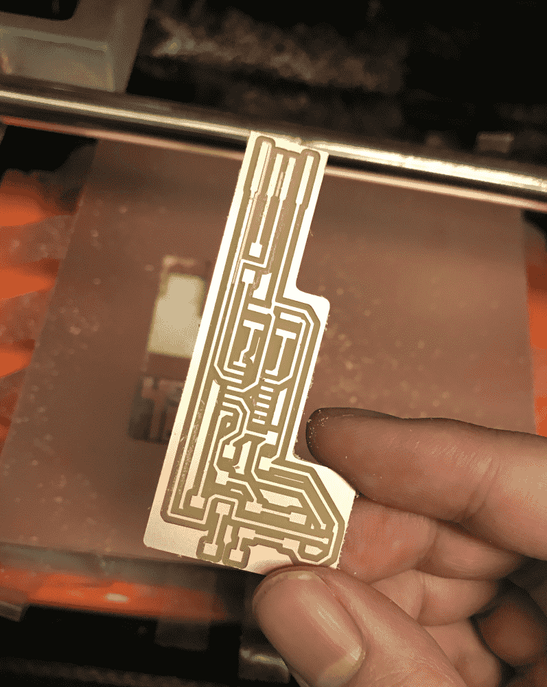
Now that I had my traces, the next step was less unfamiliar. Recalling what I learned 2 weeks ago, I stuck a board to the scrap board which was stuck to the bed in Roland SRM20. I installed the 1/64 end mill and zeroed it. I started the server and loaded my traces into mods. It didn't work because I forgot to turn the machine on. I turned on the machine, retried, and with a loud vroom it started working.
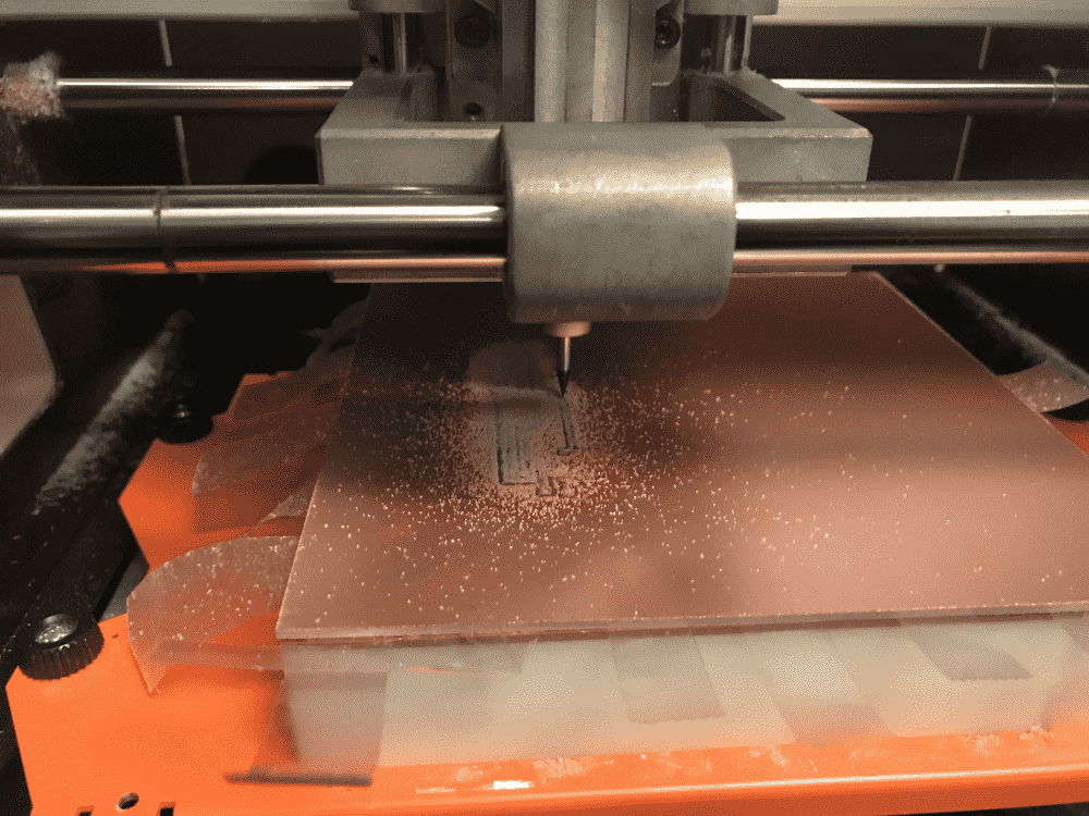
The first pass didn't quite mill through one corner of the design, which was probably because the board wasn't level enough, coupled by that my design had a somewhat large area compared to last time. So I re-calibrated the endmill near the part where it didn't go through, and re-ran. This time it came off clean.
On one hand, it is difficult to tell if the board is level by eyeballing (as far as I know, I was following the right steps to lay down the board). And the endmill only drills down by barely a millimeter, so it seems that one needs a considerable amount of luck to get a clean, moderately sized board in the first run. On the other hand, just running it twice doesn't seem to have any side effects besides extra time cost, so I guess why not?
Using the trick Neil described in class, I managed to peel off the extra copper surrounding the USB with much ease compared to last time.
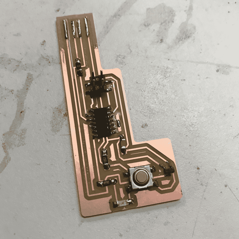
Soldering
This time less clumsy and less annoyed, I started to discover the poetic nature of the soldering experience. When the iron parted the blob, it was as if time had stopped, and the flowing solder, like water frozen, was trapped in its transient moment for eternity. Or as if under the stare of the gorgon, the slightest gestures made by the iron were petrified into silvery sculptures. A wisp of smoke fled, silently, like a sigh. But when the iron came down again, it gave back life, melting river ice in spring time, and the solder once more flowed.
There were a few parts that I wasn't sure about when stuffing. How many ohms should the resistors be? Which way is the cathode in the LED? Luckily, Zach our TA arrived just in time for office hours and helped me figure out:
- R=V/I
- Tiny green mark on the LED denotes cathode.
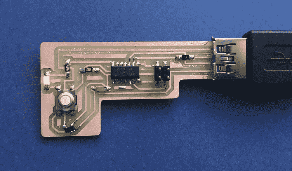
I remembered that Neil recommended using business cards for thickening the USB to improve connectivity, but I couldn't find one nearby and was keen to prove the board working, so I again smudged solder blobs on top of the 4 USB pins.
Debugging
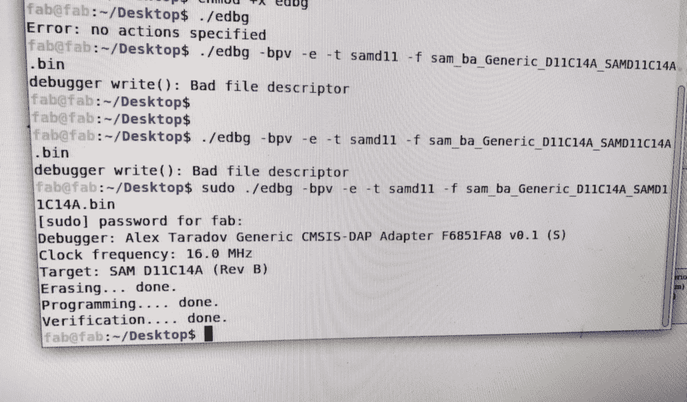
With Zach's help, I plugged the USB into my computer along with the programmer, installed edbg, and attempted to flash my board with a binary (sam_ba_Generic_D11C14A_SAMD11C14A.bin).
However, not only edbg refused to acknowledge my board, smoke also came out from the regulator, and the regulator turned brown and hot. Apparently, it was tourched. Zach did some checks with voltage meter, and advised me to replace it.
I didn't know the correct way to desolder, and while Zach was busy helping my classmates, I tried by melting the solder with the iron and lifting it with a tweezer. The problem was that there're three pins on a regulator: when I liquified the second one the first solidified again, etc. Eventually I stabbed and burnt the regulator so badly, that it shattered into pieces, and only then I was able to remove it.
I soldered a new regulator, and… it was torched again! It turned hot and brown with smoke coming out, much like the first time. Zach realized that there must be something wrong with my design!
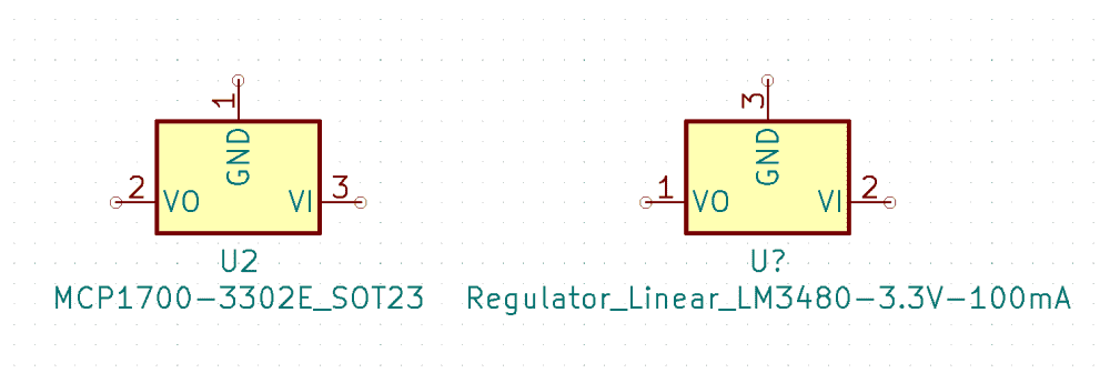
It turned out, that I placed the wrong regulator in my schematics. It was by a different manufacturer. The packaging, the schematic shape, the footprint, the physical appearance, the functionality were exactly the same, BUT, the numbering on the pins were different!! What?! What wicked person thought this was a good idea?
I thought I had to re-fabricate the board. But Zach said there was a cool hack! I could solder the regulator rotated 120°. The pins would barely touch the pads but it's still possible to do. In fact, he had to perform the same trick 3 weeks ago.
This time he also taught me the correct way to desolder, which was to lift the board with a tweezer by the part to be removed, and to blow it with a hair dryer.
With some patience, I soldered a crooked regulator onto my board. It didn't look ugly -- it gave some dynamism and flavour to the otherwise axis-aligned parts.
However, edbg was still giving the error message, claiming to not have received valid response from the board. Zach tested the board on his Linux machine, and it turned out that the board was working! The problem was either with my mac or my edbg installation.
So I used the Linux machine in the PCB shop to flash my board. I did some commandline frobbing and all went smoothly. I have my board!
Programming
I completed the fabrication and flashing on Saturday and was planning to visit Zach's office hours again on Sunday, to learn about how to program the board to do something.
However, it occurred to me that many of my classmates were still struggling with finding the correct parts and drawing the schematics. I thought they would need the TA's help much more than I do; plus I already received a lot of help on Saturday. Therefore, I thought it would be more moral (and fun) to figure out the programming part on my own.
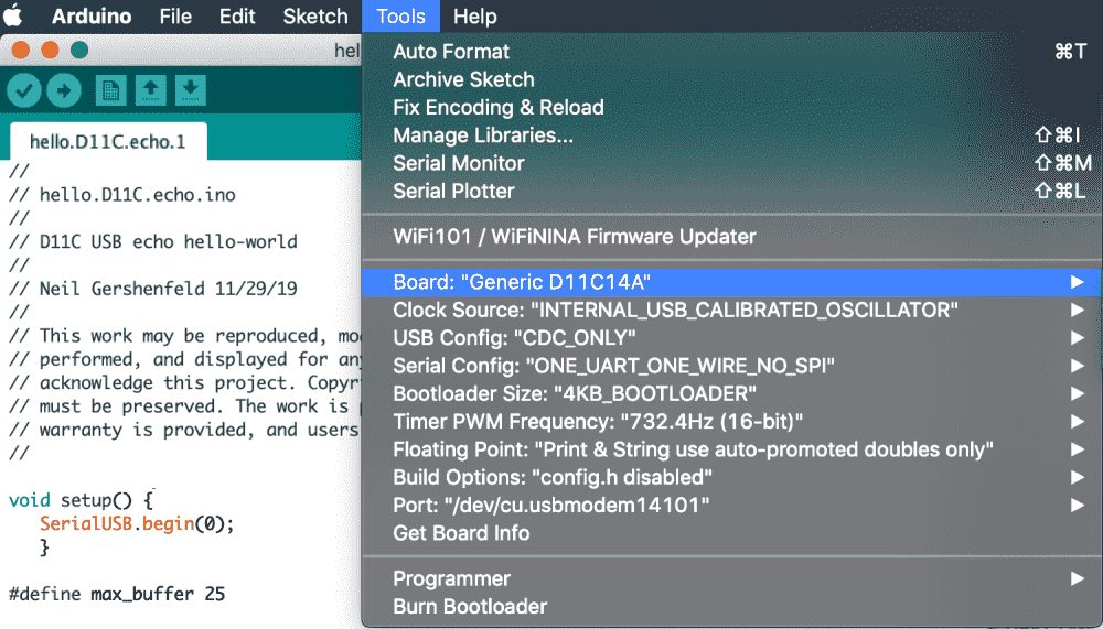
Initially I had no clue, but then I discovered the "SAMDino" post by Adrián Torees linked on the course website, which gives clear explanation on how to use the Arduino IDE to program a SAMD11C board. I also took a peek at the echo.ino program and the accompanying video on the course site.
The process involved adding this board manager URL and downloading the “board package” (which I assumed to be similar to installing a software library) in Arduino IDE. Then specify the right board (SAMD11C) and the port in the menu. The rest was just plug and play!
Just moments later I got the LED and the button on my board hooked up to my program, so that when I press the button, the LED lights up.
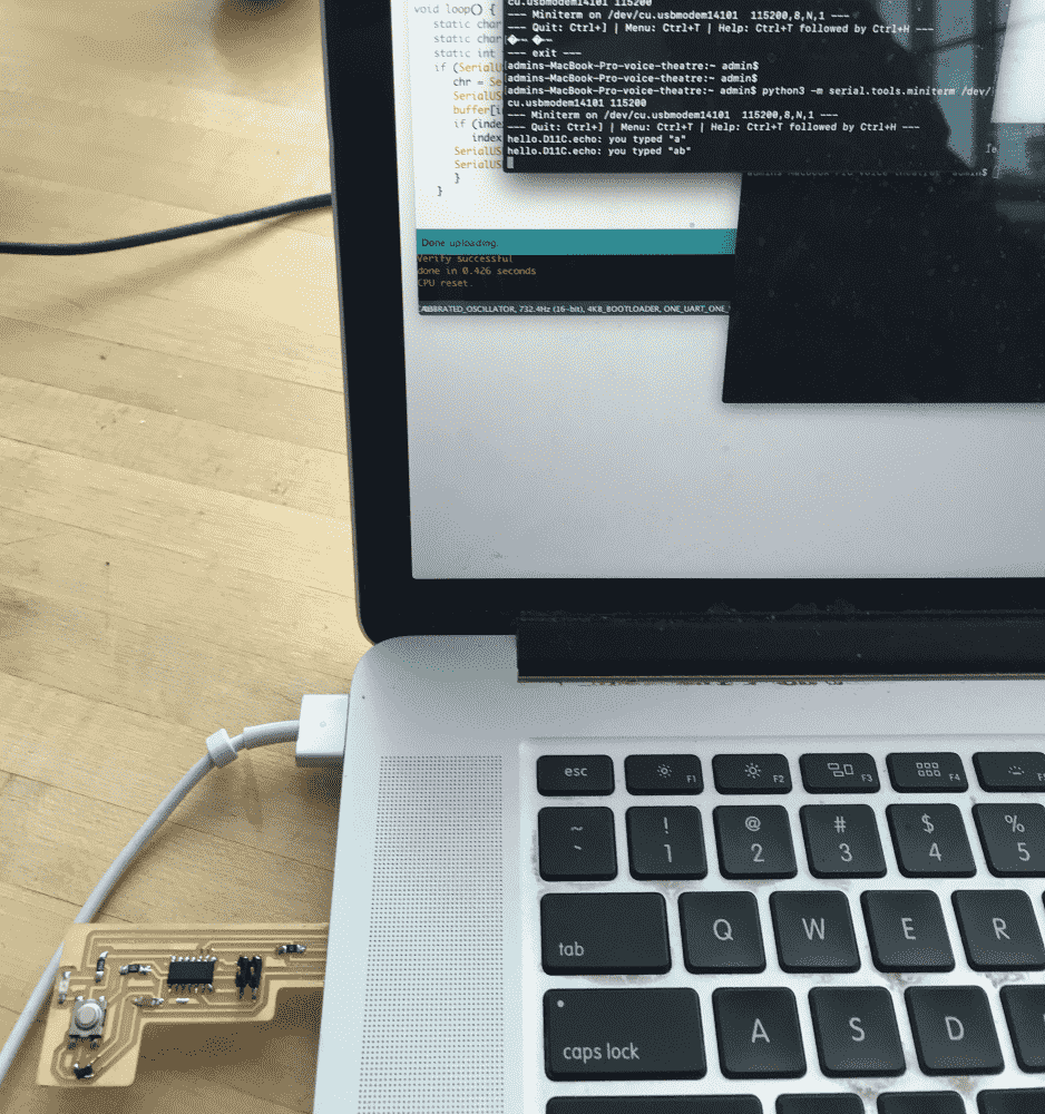
I was so happy. I've been programming very complex things for some years but somehow, just lighting up a LED with a button still made me so happy. I never felt so happy for a while. I guess it's partly due to all the troubles I went through, from designing to fabrication to debugging etc.
Naturally now I wanted to do something cooler than a light switch. But limited to 1 button and 1 LED, what could I make?
While thinking, I ran all the way to microcenter and bought myself some cheap USB hub and extension.
After I came back, I wrote a calculator that could be operated with 1 button, and output results with 1 LED. The user enters the numbers to be added, digit by digit, in binary, with a long press indicating a one, and a short press indicating a zero. The board outputs the result by blinking: a long blink means one, a short blink means zero. A super long press of the button indicates end of input, switching the state from entering the first number to that of the second, and from the second to read out.
In the video below I demo my calculator. (Note that when the user is inputting the numbers, the LED goes off when the button is pressed; this way the LED is always on while idle, making it easier to notice the board is working. However, it might look a bit confusing to spectators watching the video, especially since the button is obscured by the thumb pressing it).
I guess it is probably the most useless calculator ever, because converting numbers into binary and back is a more difficult task for most human beings, than adding two numbers together.
You can find my code below:
// calculator.ino

int n_int_bits = sizeof(int)*8;

const int pin_led = 4;
const int pin_btn = 2;

int btn_state_prev = HIGH;
int btn_state_curr = HIGH;
int btn_down_t0 = -1;
int btn_down_dt = 0;

int btn_thresh_super_long = 1800;
int btn_thresh_long = 700;

int nums[2] = {0};

int mode = 0;

int result;

void print_msg(String s) {
  if (SerialUSB.available()) {
    SerialUSB.print("["+String(mode)+"] D11C says:  ");
    SerialUSB.println(s);
  }
}

void setup() {
  pinMode(pin_led, OUTPUT);
  pinMode(pin_btn, INPUT);
  SerialUSB.begin(0);

  re_init();
}

void re_init(){
  mode = 0;
  digitalWrite(pin_led, HIGH);
  nums[0] = 0;
  nums[1] = 0;
  print_msg("ready.");
}

void btn_down(){
  print_msg("btn down");
  digitalWrite(pin_led, LOW);
  btn_down_t0 = millis();
}

void btn_up(){
  print_msg("btn up");
  digitalWrite(pin_led, HIGH);
  btn_down_dt = millis() - btn_down_t0;
  print_msg("(was down for "+String(btn_down_dt)+"ms)");


  if (mode < 2){
    if (btn_down_dt > btn_thresh_super_long){
      print_msg("next state");
      mode++;
    }else if (btn_down_dt > btn_thresh_long){
      print_msg("entered 1");
      nums[mode] = (nums[mode] << 1) | 1;
    }else{
      print_msg("entered 0");
      nums[mode] = (nums[mode] << 1);
    }
  }
  print_msg("curr num: "+String(nums[mode]));
}

void update_btn_states(){
  btn_state_curr = digitalRead(pin_btn);
  if (btn_state_curr == HIGH && btn_state_prev == LOW) {
    btn_up();
  }else if (btn_state_curr == LOW && btn_state_prev == HIGH){
    btn_down();
  }
  btn_state_prev = btn_state_curr;
}

void blink_short(){
  delay(150);
  digitalWrite(pin_led, HIGH);
  delay(400);
  digitalWrite(pin_led, LOW);
  delay(150);
}

void blink_long(){
  delay(150);
  digitalWrite(pin_led, HIGH);
  delay(1000);
  digitalWrite(pin_led, LOW);
  delay(150);
}

void readout(){
  int i, d, skip = 1;
  digitalWrite(pin_led, LOW);
  result = nums[0] + nums[1];
  print_msg("result: "+String(nums[0])+"+"+String(nums[1])+"="+String(result));

  delay(2000);
  for (i = 0; i < n_int_bits; i++){
    d = (result >> (n_int_bits-1-i) ) & 1;
    print_msg("bit "+String(i)+"="+String(d));
    if (d){
      skip = 0;
      blink_long();
    }else if (!skip){
      blink_short();
    }
  }
  delay(2000);
  re_init();
}


void loop() {

  update_btn_states();

  if (mode == 2){
    readout();
  }
}
Perhaps not my neatest program, but it works!
I noticed that the Arduino IDE reported that I was using 94% of the 12K total storage space. I wonder how much of that is generated bloat compiling from .ino, and if I could directly program it in C or assembly? I'm interested in fitting complex programs in small storage. I guess it's definitely possible; Perhaps it involves edbg, and some specialized version of gcc. Hopefully I'll learn how to do that in the coming weeks!
Downloads
My design files and outputs can be downloaded below: