This week, we had to program our board to do something. The board I made didn't really work, so I had to get help to make a basic board. The electronic components part of this course has been incredibly difficult for me to understand. I started from the basics in order to build up my foundational knowledge. The first step involved understanding the function of the components. I've linked the video that proved most helpful below:
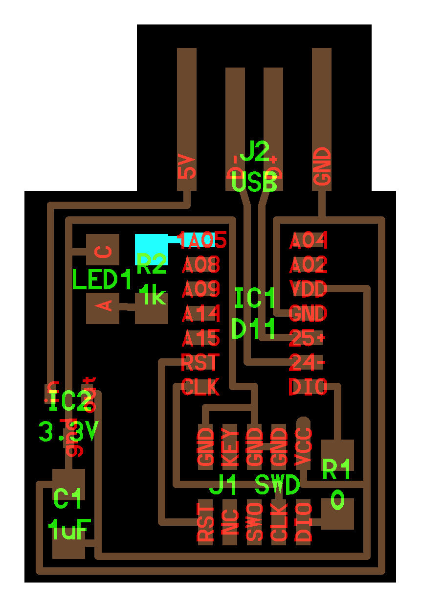
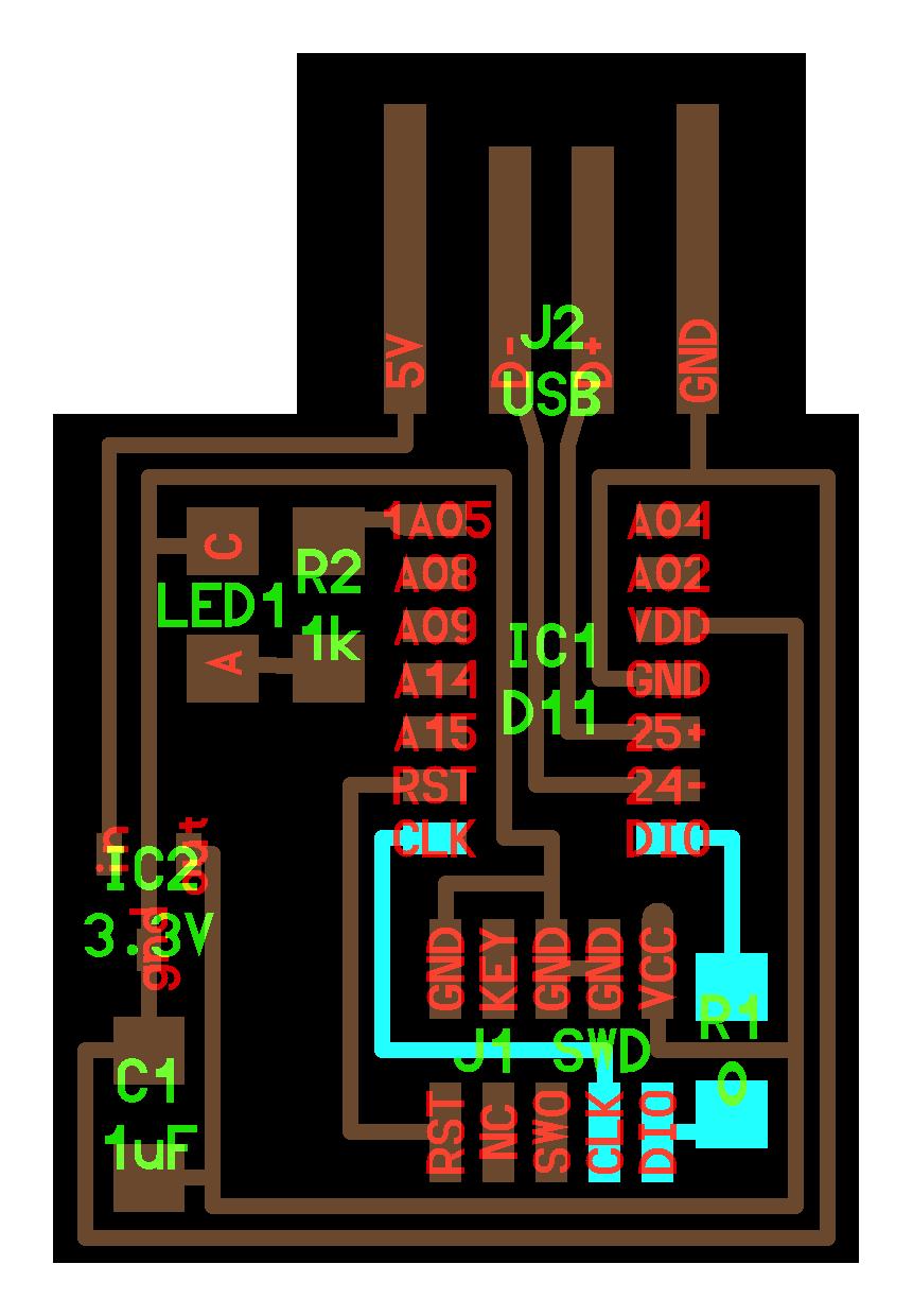
Beyond understanding the basic components, I had no idea about the layout of components on a board. I tried to "trace" the traces from the SAMD11C and ATtiny1614 in order to make sense of things (since those were simpler than the ESP32). One of the most important things in retrospect was referencing the datasheet for the microcontrollers. The placements of connections felt arbitrary before looking at the data sheet.
Reading through the schematics posted on the course website prove nearly inpenetrable at first. I am not sure whether I am alone on this, but I thought I should document my learning process.
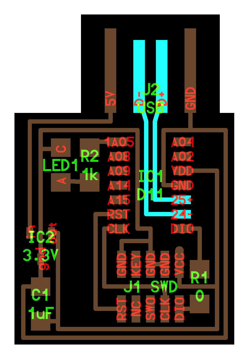
Based on my tracing, I found there to be three main "tracks" when building a circuit board: (1) Sending Power; (2) Debugging/Programming; and (3) Adding components.
I started with power. I looked at the D11C schematic, since I knew the power was coming from the USB connection. So I traced the 5V connection down to its first destination.
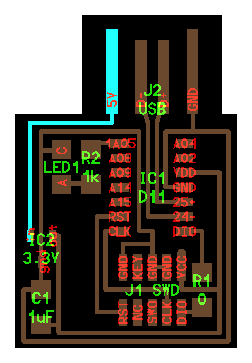
That led me to the voltage regulator. The voltage regulator is rated for 3.3V, and there is an input, output and ground pin (based on the completed version). The input pin was connected to the power 5V source. But how do we know to get a 3.3V regulator? Good question! That wasn’t known to me until I looked at the datasheet. The one for D11C is almost 1,000 pages, but thankfully the specifications are at the top. There is a part that talks about operating specifications, which is between 1.62V and 3.63V. 5V is outside that range, so we just needed any voltage regulator rated in between that range. Looking at the trace, the out pin of the voltage regulator should connect to a capacitor and then to the other
components that need power. The capacitor helps with consistency I guess?
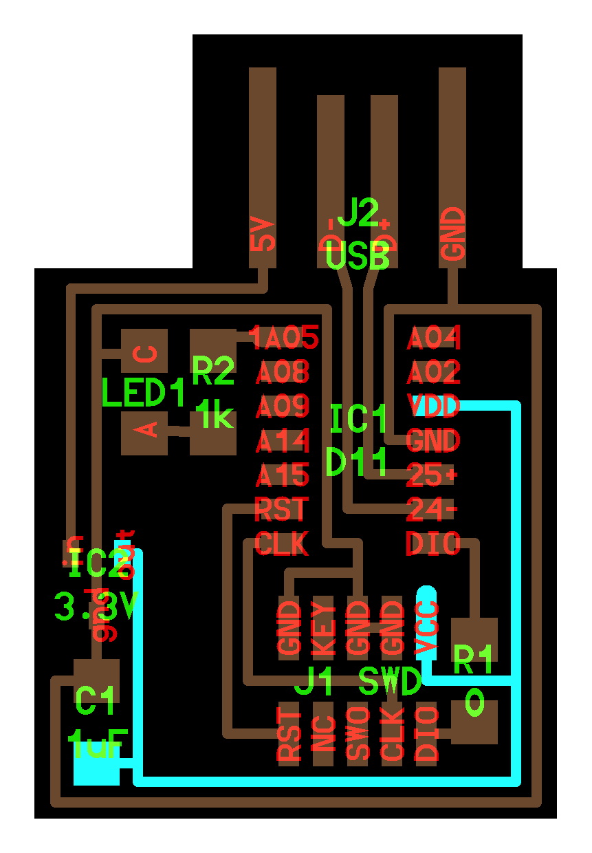
Notice that the capacitor touches at two points on the board. The part that receives the regulated voltage is also directly connected to the other components that need power. There are pins specifically for power on the serial/debugging/programming components and the microcontroller. For the microcontroller, these can be found in the manual. The SWD/FTDFI/USB all seem to have standard orderings (so you can replicate what is on the hello boards). The capacitor node that isn't directly connected to the voltage regulator is grounded.
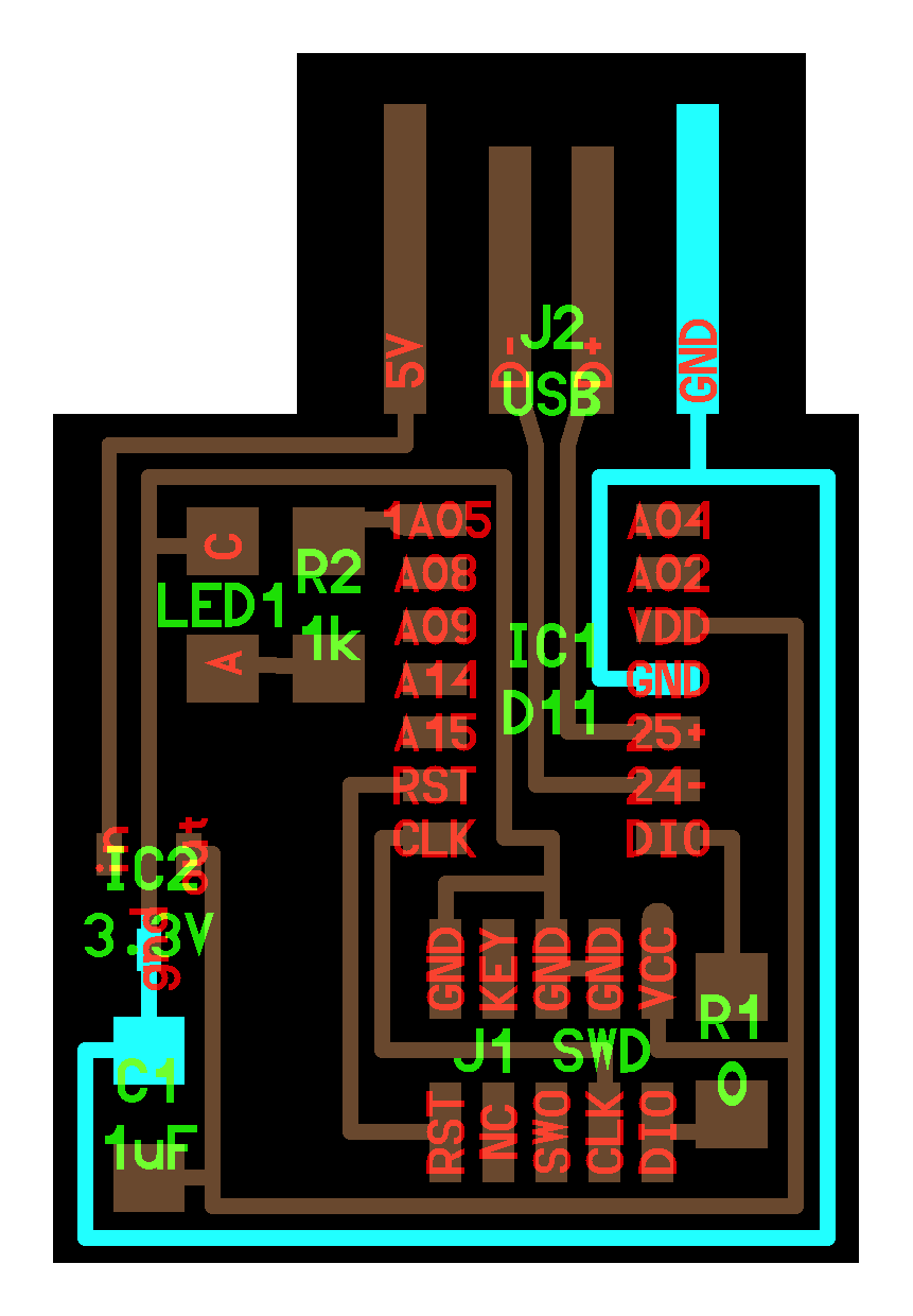
There were certain components that had grounds connected to that side of the capacitor, including the debugging/programming/serial components, the microcontroller, and the voltage regulator. In practice, I think the rule is just that things need to be grounded to some common connection. For example, if we trace the LED connected PIN, we can see that the LED is also grounded to the SWD component:
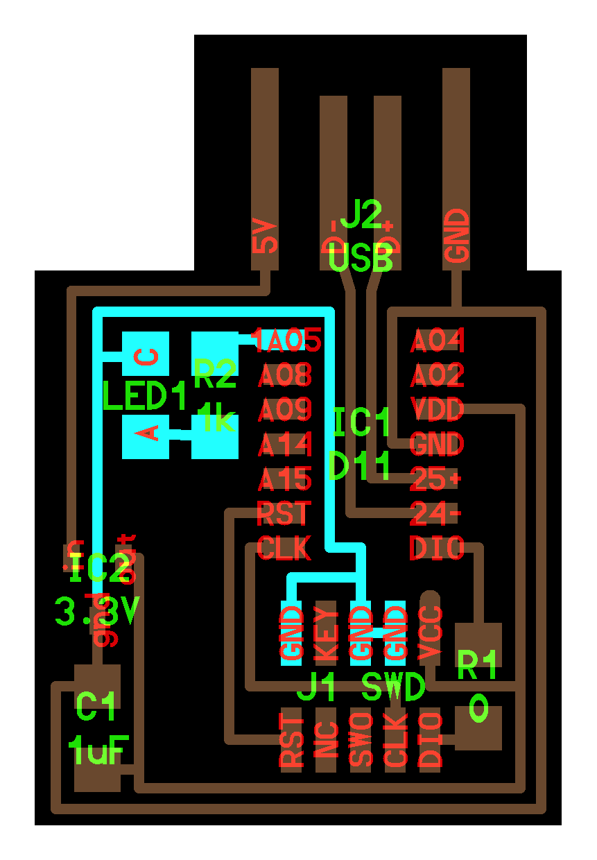
If we go slightly back, we also see that LED components need a resistor (either before or after the connection).
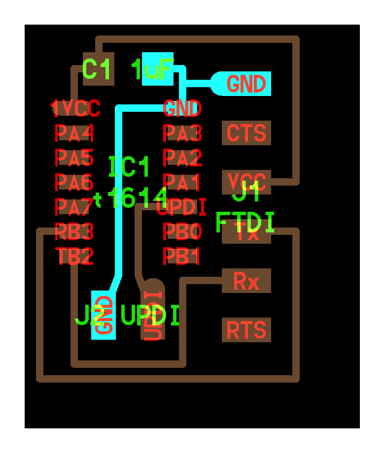
The ATTiny doesn’t have a voltage regulator. I thought this ruined the inductive learning, but then I checked the manual and saw that 5V is within the operating range. So a regulator wasn’t needed. It was still the case that the capacitor received the source power (in this case, coming from the FTDI component and not USB).
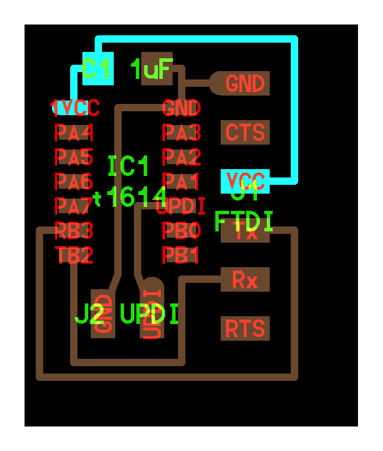
Here, we also see that the grounds are connected:
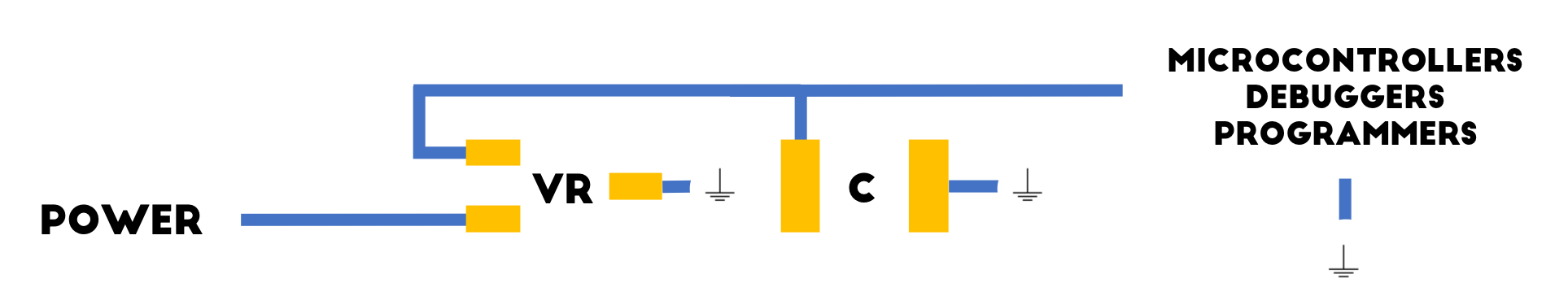
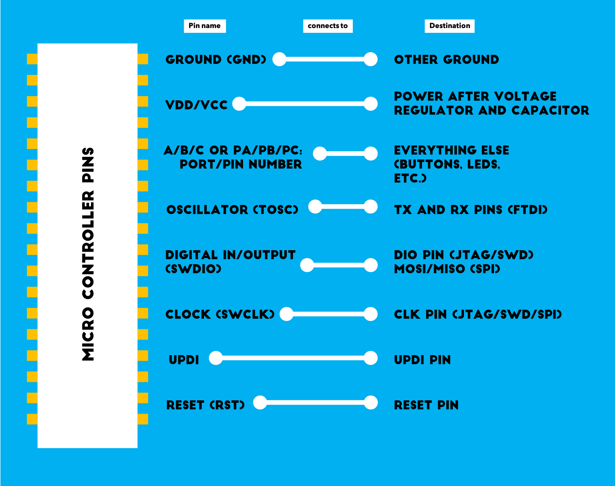
Based on these observations, I made a diagram to help myself when designing a circuit board:
Debugging, programming and serial communication were even more confusing to understand because the two boards were using different Programming components. But what even is programming and debugging? I think the simplest answer is making and transferring software (the program) from one device (like my computer) to another (the board). The components on the board are used in order to allow that transfer to happen. It seems like there are two things a board might need. The first is a serial component, which allows communication between your computer and the board (the component also supplies power). This is accomplished through USB/TTL, or FTDI when there is no USB/TTL port on the board. Starting with USB on the D11C, I saw that there were D+ and D- pins connected to pins on the microcontroller.
Reading through the pins diagram in the D11C datasheet, the pins that D+ and D- were connected to seemed to
just be non-descript digital pins.
Next, the FTDI on the 1614. There were two pins that weren't connected to anything else on the board. These were CTS and RTS (the latter I think should actually be DTR based on diagrams I looked at).
.png)
These seem to just indicate to the computer that the device is ready to communicate and transfer data. Next, the FTDI had Tx (Transfer) and Rx (Receive) pins. These pins transfer and receive data. Looking at the 1614 data sheet, it looks like the Tx and Rx pins on the FTDI were connected to OSC (oscillating/clock crystal pins). This has something to do with the internal clock. I'm not sure what they specifically do, but I guess it's good practice to link the Tx and Rx with the OSC Pins on the microcontroller. There also seem to be 2 oscillator pins on the D11C, so I'm pretty confident that this is a good convention.
Adding everything I learned together, I created this diagram for my personal reference:
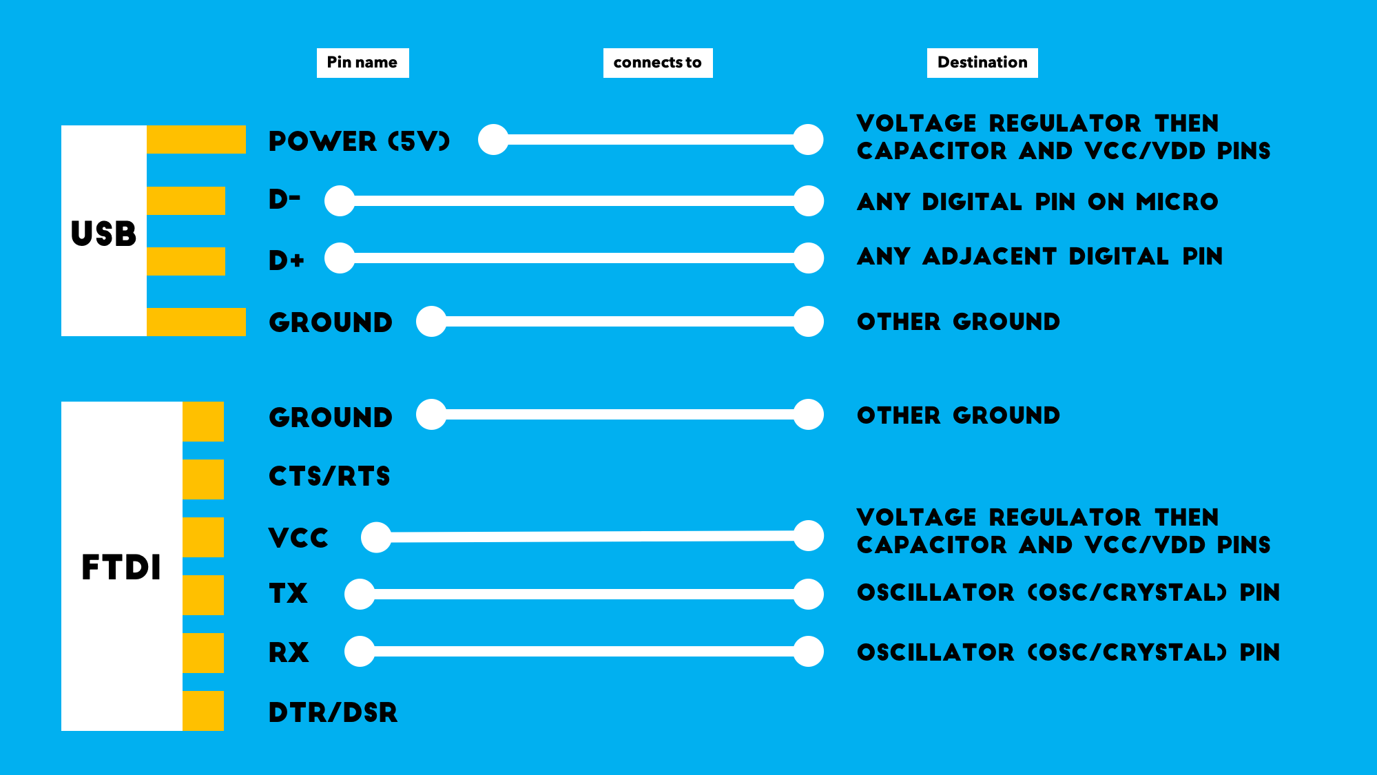
The second thing a board needs is a component that allows you to debug and program things onto the board. The components that enable this are things like JTAG/SWD, SPI, UPDI, etc. These things need power it seems, so they may have VDD/VCC ports.
Starting with SWD/JTAG on the D11C. JTAG (and its alternative SWD) are debugging and programming interfaces for a circuit board. They have 10-pin and 20-pin versions, and the layouts are standard (so, thankfully, you only need to understand it once). For the 10-pin, the top row has three grounds, a key (which just helps you see the position of the component) and a VCC (power connection).
A SWD/JTAG also has a reset pin, which is connected to the microcontroller's reset pin.
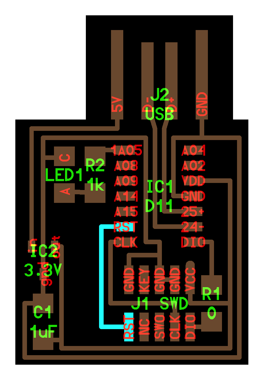
This does what it sounds like: restarts/resets the board.
In order to transfer information between the board and the computer, SWD and JTAG has DIO (Digital Input/Outpit) and CLK (Clock) pins on the bottom row:
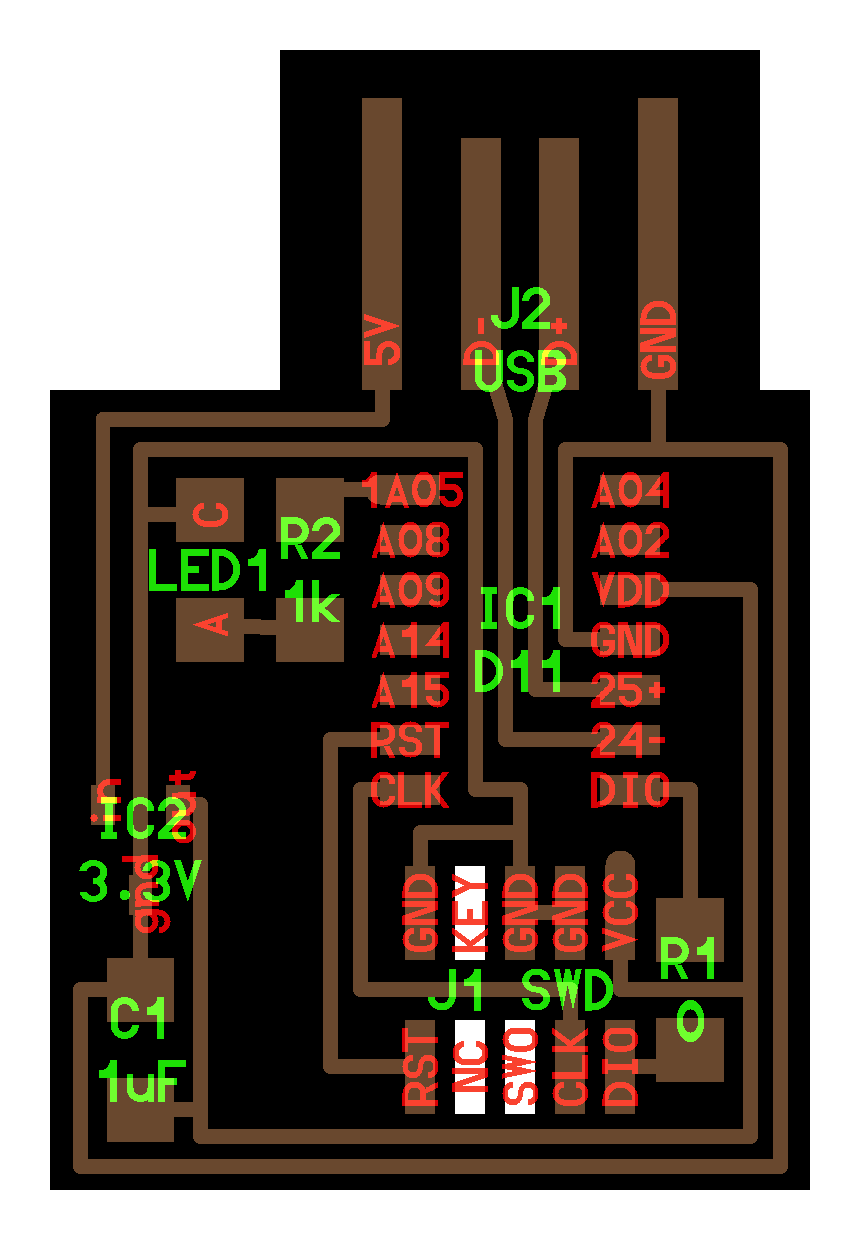
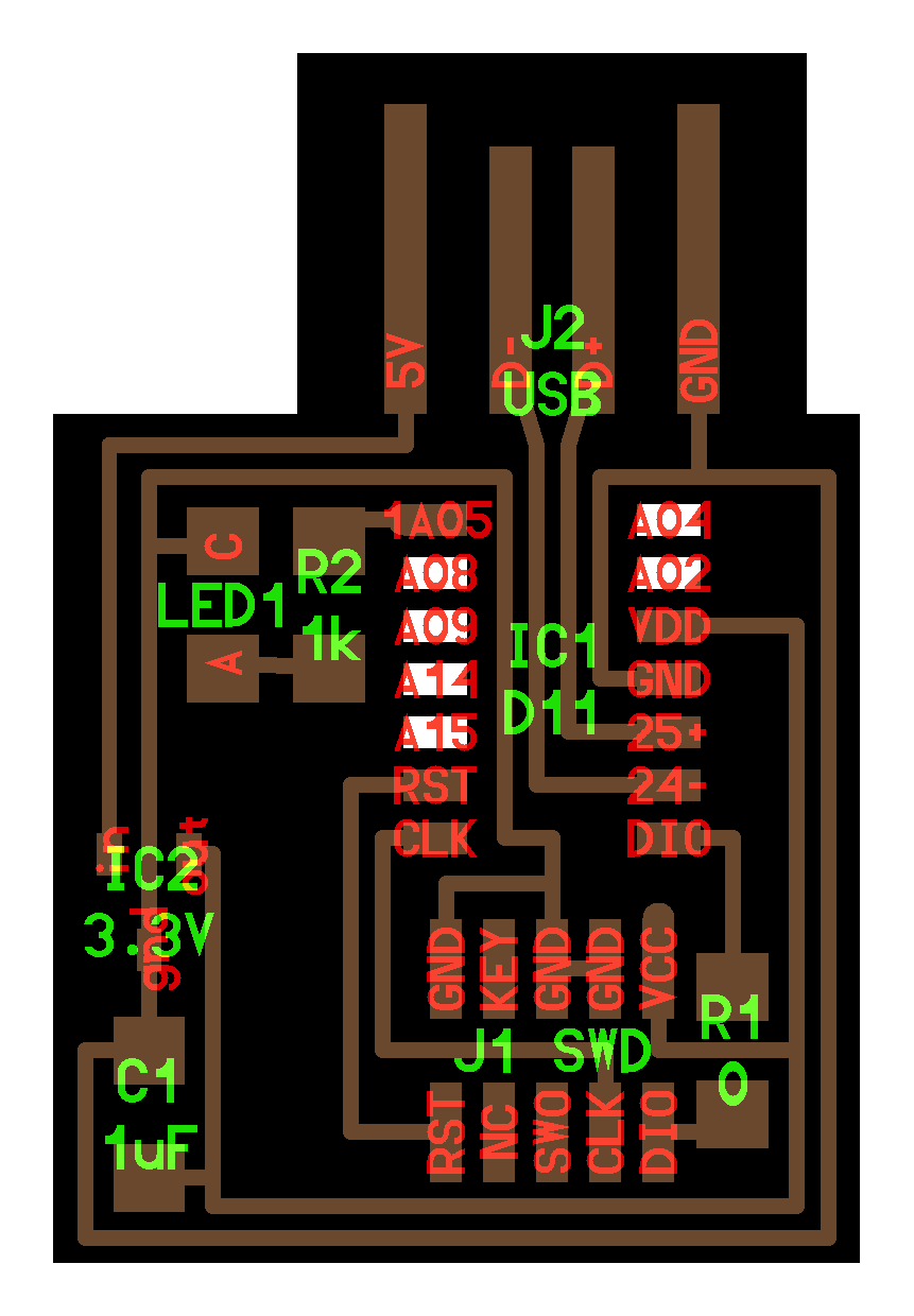
I had to dig a bit in the D11C data sheet to find whether there are pins specifically for SWD/JTAG. There are: Pin 30 is SWCLK (which connects to CLK on SWD/JTAG) and Pin 31 is SWDIO (which connects to DIO on SWD/JTAG). Your mileage may vary with other microcontrollers. The SWO and NC pins aren't connected to other things on the board. As mentioned before, the KEY pin doesn't do anything except let you know which way the component is.
Next, the UPDI interface on the 1614. This one is fairly simple, since the UPDI pin only has one connector:
.png)
There is a UPDI/RESET pin designated on 1614 (check the data sheet).
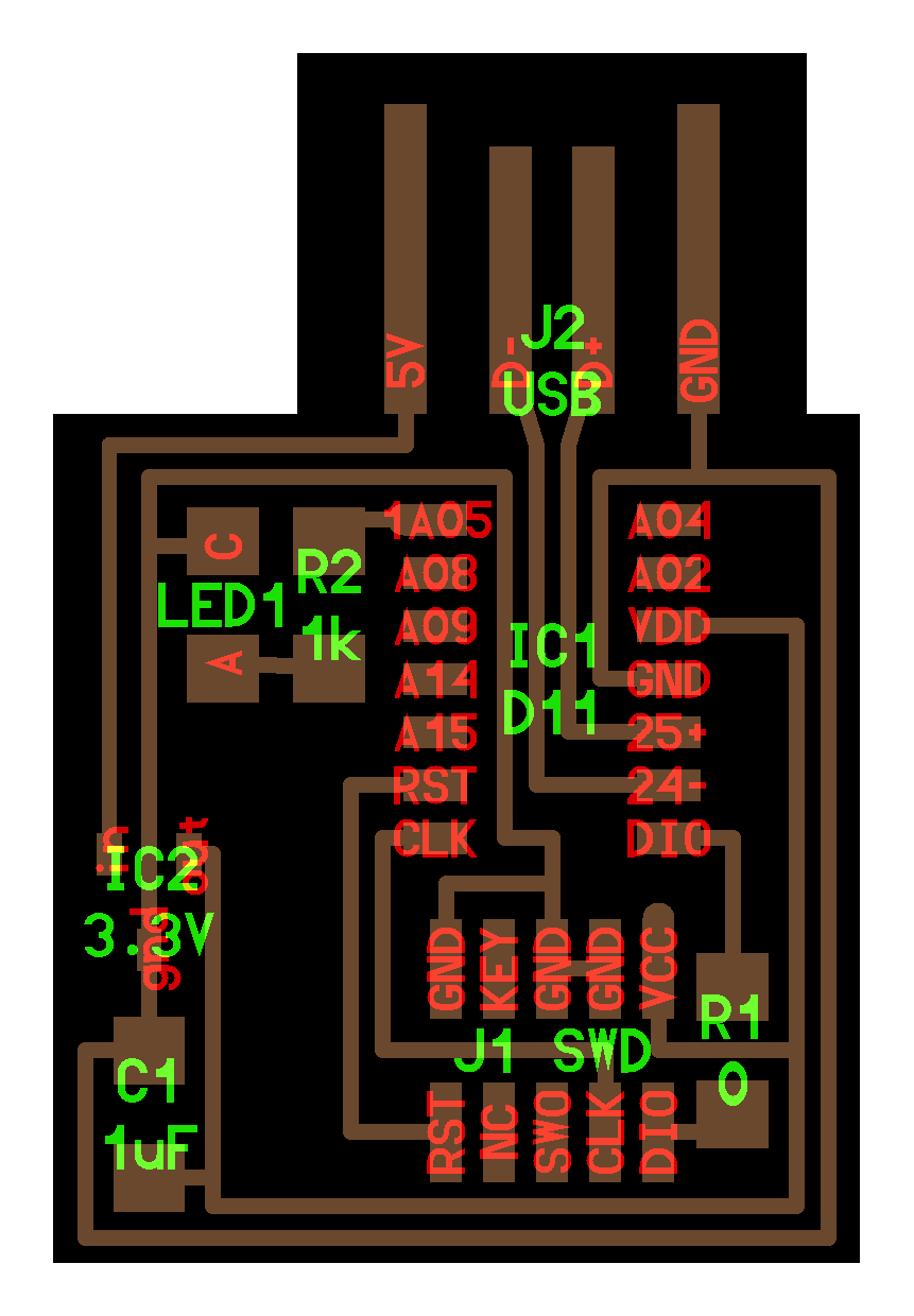
Next, comes adding components. Even after adding serial and programming components, there are still plenty of pins on the D11C microcontroller.
These pins are probably where other components (LEDs, buttons, etc.) are located. I think it might be possible to add a button on any of these ports. The main challenges then are positioning the part on the board so that its connection trace isn't too complicated and/or space-hogging and choosing between an analog or digital pin. Digital pins are for ON/OFF or HIGH/LOW components (like a button), whereas analog takes on many values. I made one more diagram to help me understand what needs to be connected to the microcontroller before I start adding things:
Once I get my board, working, I can put this all into practice. I think for the next few weeks, I want to work on creating the fan modules for my final project. I think having a temperature sensor that triggers the fan would be doable given my skill level.
Since we had to program our board to do something, I decided to use a stepper motor module. I wanted something cheap that only consumed 5V. I decided on the popular 28BYJ-48, since it had a lot of helpful documentation online. I realized that stepper motors also required separate driver boards. This was the module available.
Stepper Motor Module
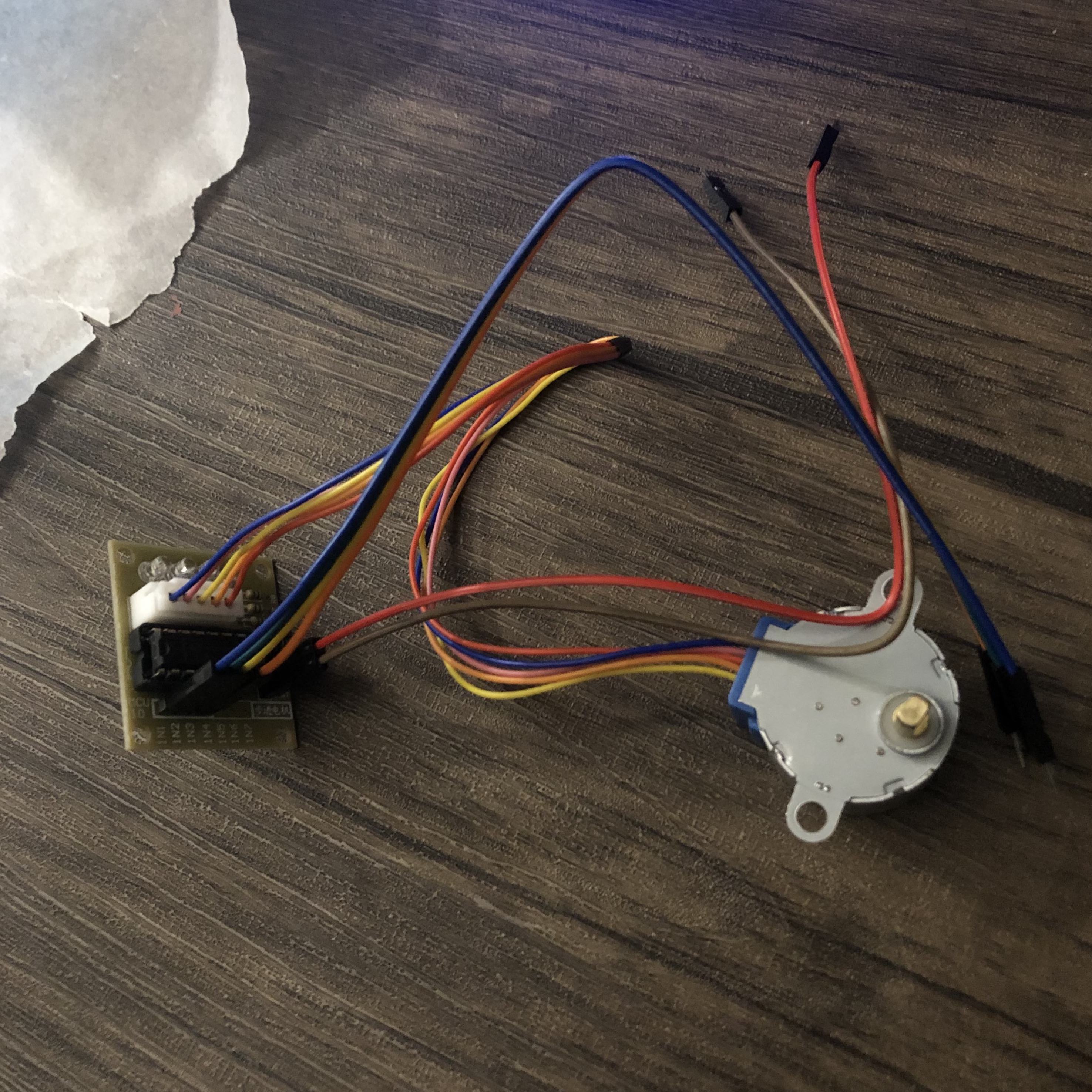
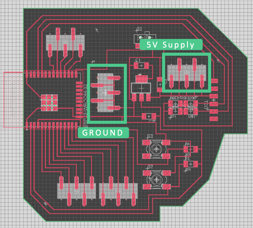
On top of needing a 5V power supply, there were four separate components that needed to be controlled by my board. Because my board had both ground and 5V connectors, this was fairly simple (see Week 5 for the board schematics and download)
My board
I had to remember to switch the board into programming mode and reset the board. There were two Arduino sketches that I had, based on the stepper motor manufacturer example and an Arduino example.
You can actually see the white LED blink as the board is being programmed:
Programming Blinker
At first I was nervous because nothing was happening, but that was because I forgot to take it off programming mode. The stepper motor worked!
Slow Rotation
Word of warning for the next time: I need to get a separate 5V power supply. Thankfully my board wasn't ruined, but I think I messed up my USB port on my laptop because the motor drew too much power.