Week 05 — Electronics Production
Milling, Soldering & Testing the Sun PCB
Overview
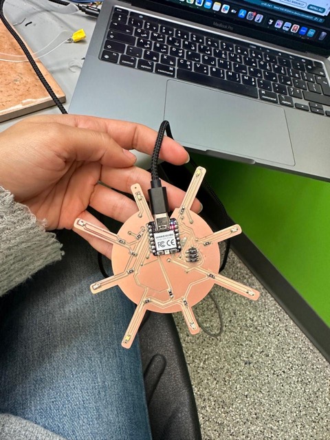
This week, I fabricated and programmed my sun PCB designed in Week 04. The process involved milling the board on the Other Mill, hand-soldering tiny SMD components, and debugging electrical connections to bring the design to life.
Learning Objectives
- Group Assignment: Characterize the design rules for in-house PCB production process
- Individual Assignment: Make and test an embedded microcontroller system that you designed
- Extra Credit: Make it with another process (laser/vinyl)
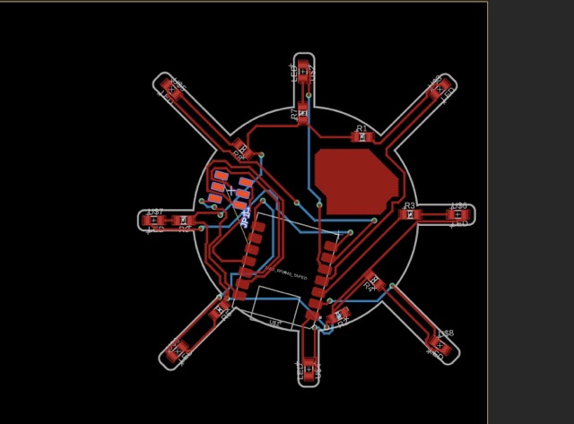
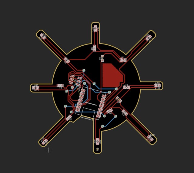
PCB Design from Week 04
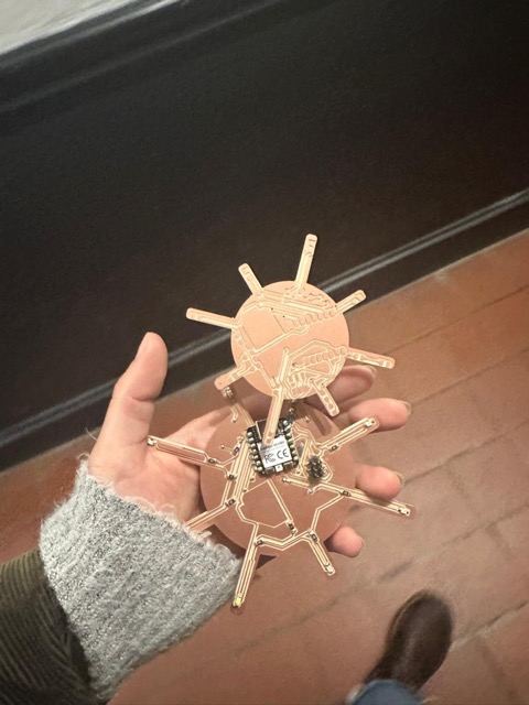
I designed a sun-shaped PCB pendant with a Xiao RP2040 microcontroller and eight LED rays. The design includes a 3×2 connector for future inputs/outputs (capacitive touch will be implemented during Input Week). This was designed in Fusion 360 Electronics.
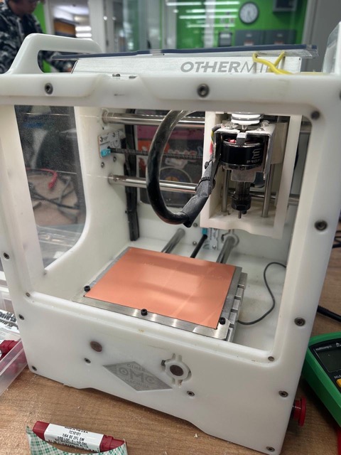
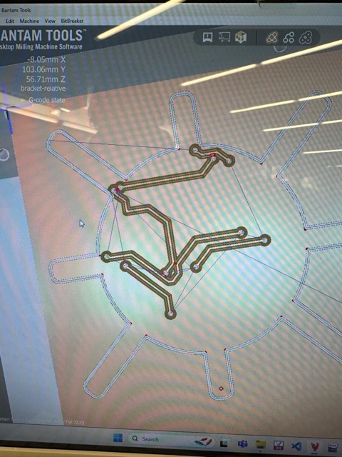
Milling on the Other Mill
I used the Other Mill (Bantam Tools) to mill my PCB on FR-1 board material. The Other Mill has a good UI and runs native .brd files from Fusion 360 Electronics.
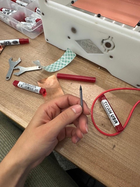
Other Mill Setup Process
- Home the machine: Press "Start Homing" - the mill drives and figures itself out
- Load file: Open .brd file (Fusion/Eagle format) or Gerber files
- Prepare board: Cover entire FR-1 board with tape, align left-justified
- Set placement: X-Y position with 1mm buffer from edges
- Tool setup: Start with 1/32" PCB end mill for traces, then 1/64" for tight spots
- Locate tool: Use locating bracket to set Z-height (FR-1 = resin & paper stiffened)
- Start milling: Mill all visible layers - the software highlights areas where tools can't reach
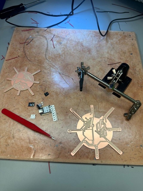
First Attempt - Misalignment Issues
My first mill was unsuccessful due to misalignment between the top and bottom layers. When milling double-sided boards, precise alignment is critical, and I struggled to get the fixture positioning correct.
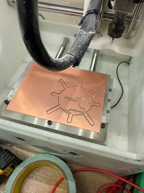
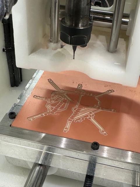
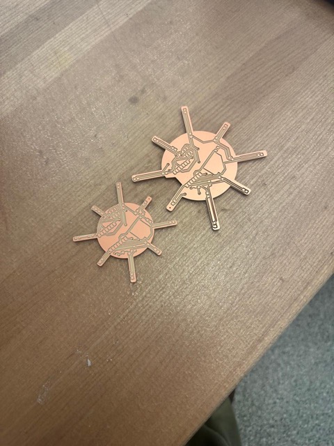
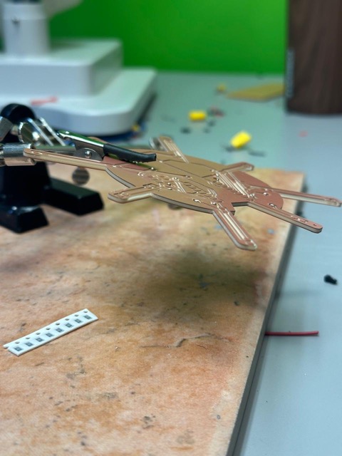
Second Attempt - Success!
For the second attempt, I went bigger with the board outline and cut a space for the USB connection so I wouldn't need to move the microcontroller position (which would have required rerouting everything). This strategic redesign worked!
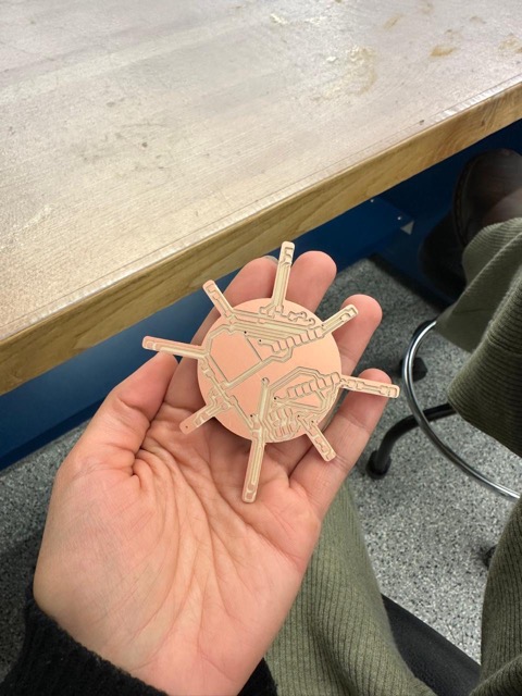
PCB Design Iteration
After the milling challenges, I made design improvements to give components more space and improve routing (the paths that electrical nets take on the board). The rays shooting out from the sun center needed wider traces for easier milling.
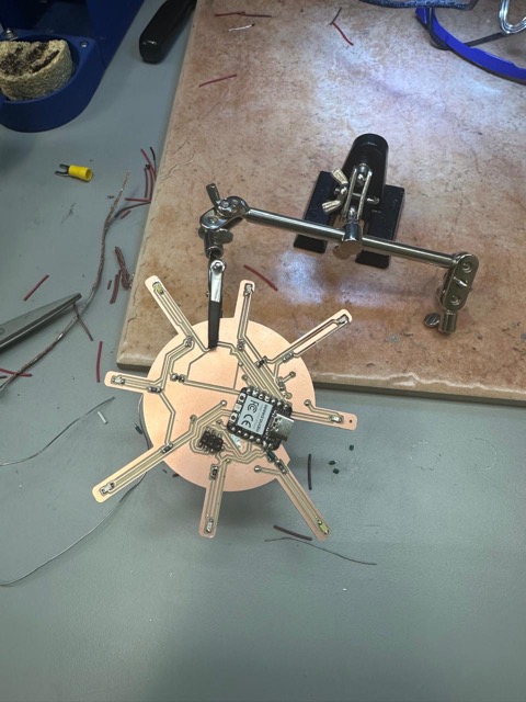
Soldering & Debugging: The Learning Curve
After milling, I moved to component assembly. This was my second time soldering but my first time soldering a board I designed myself. Following my own schematic and making sure everything was correct required much more careful attention and debugging than soldering someone else's design. It turned into one of the most challenging—but educational—parts of the week.
Components from My Schematic
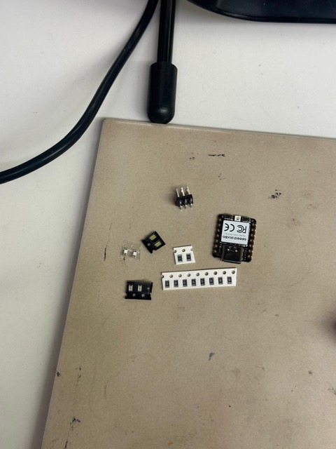
- 1× Xiao RP2040 module: The microcontroller brain
- 8× LEDs (0603 package): Tiny surface-mount LEDs for each sun ray
- 8× 470Ω resistors: Current limiting for LEDs (gives soft glow)
- 2× 0Ω resistors: Jump resistors for routing
- 1× 3×2 connector: For future inputs/outputs (capacitive touch in Input Week)
Initial Soldering Process
I started by soldering the Xiao RP2040 using flux, tacking corners first, then running solder along the castellated edges. Then I placed the tiny 0603 LEDs and resistors.
The Debugging Marathon
After soldering everything, I plugged in the board expecting it to work—but nothing happened. This began hours of troubleshooting with the multimeter (the "probe meter thing" that became my new best friend).
What I Learned About Multimeter Testing
The multimeter became essential for debugging. I used it to:
- Continuity mode (beep test): Check if traces were actually connected where they should be
- Voltage mode: Verify 3.3V was reaching the LED pins
- Resistance mode: Check if resistors were the correct value and properly soldered
- Diode mode: Test LED polarity and verify they weren't burned out
Key realization: Just because solder looks shiny doesn't mean there's electrical connection—cold joints are real!
Challenge 1: LED Orientation
The problem: Some LEDs weren't lighting even though voltage was reaching them. I spent a long time checking my code before realizing the issue was hardware.
The lesson: LEDs have polarity! The flat edge/short leg is the cathode (negative), and it must connect to ground. I had accidentally placed a few LEDs backward. Once I desoldered and flipped them, they worked immediately.
Learning curve win: I can now identify LED orientation by looking at the green markings inside the package (cathode side is bigger) without needing to find the flat edge every time.
Challenge 2: Ground Connections & Vias
The problem: Even with correct LED orientation, entire sections of my board weren't lighting. The multimeter showed no continuity between LED grounds and the main GND plane.
The lesson: Ground is not magic—it's just another trace that needs physical connection. My double-sided board had some vias (plated through-holes) that didn't make proper contact between top and bottom copper layers. The rivets were the main challenge - I had to make sure they weren't just topped up with solder on the surface, but that the solder was actually touching and connecting the copper traces on both sides.
Solution: I had to use a jump wire for the first time to manually bridge ground sections, and I filled the vias with more solder to create proper electrical connection through the board layers.
Big win: Understanding that GND = 0V reference and that all grounds must be electrically connected was a major "aha!" moment. It's not enough for them to be labeled GND—they have to physically touch through copper or solder.
Challenge 3: Cold Solder Joints
The problem: Some LEDs would flicker or work intermittently. Visual inspection looked fine.
The lesson: A cold solder joint looks dull and grainy instead of shiny and smooth. The multimeter's continuity test (beep mode) was crucial here—I'd probe each LED pad and discover the solder looked connected but wasn't making electrical contact.
Solution: Reheat the joints properly: heat the pad AND component pin together, add a tiny bit more solder with flux, let it flow smoothly. The joint should be shiny and cone-shaped, not blobby.
Debugging Workflow I Developed
- Visual inspection first: Look for obvious bridges (solder connecting two pads that shouldn't touch)
- Continuity test: Beep test from microcontroller pin → resistor → LED → GND (should be continuous path)
- Voltage test: Power on board, measure voltage at each LED pin (should be 3.3V when code sets it HIGH)
- Component test: If voltage is correct but LED doesn't light, test LED in diode mode (might be reversed or burned out)
- Incremental fixing: Fix one LED at a time, test immediately, don't batch fixes
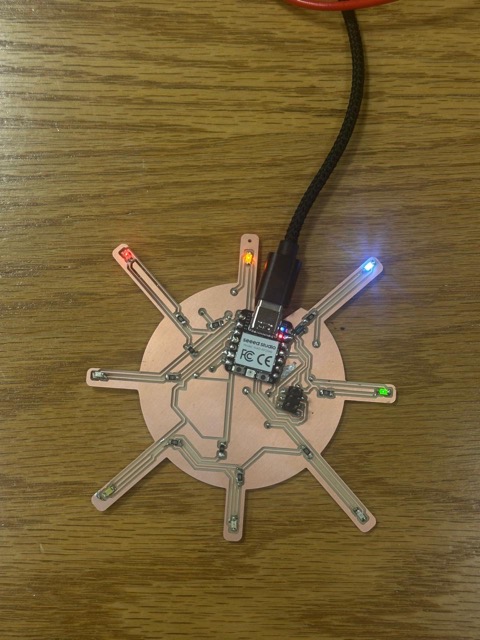
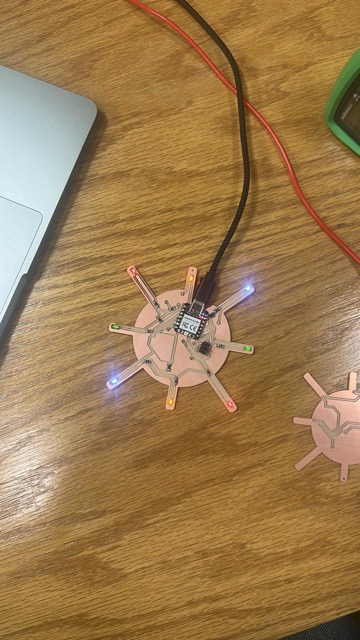
Success!
After several rounds of debugging and rework, all LEDs finally lit up! The soldering took much longer than expected, but I learned more in those few hours than I could have from just watching tutorials.
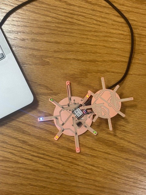
Beginner wins: Understanding LED polarity, ground connections, cold joints, vias, rivets, and multimeter debugging are fundamental skills that I'll use forever. I'm genuinely surprised at how much there was to learn—and grateful for the troubleshooting practice.
Programming & Testing
With the board assembled and debugged, I programmed the Xiao RP2040 to control the LED rays. The goal is to create a ping-pong chase animation that lights each LED in sequence, forward and backward.
Learning Process: I had help from ChatGPT to get started with the Arduino IDE sketch, and then I asked it to walk me through the code step by step. Once I understood the code structure more or less, I tested many different sequences and modified the patterns to create the final ping-pong animation. This hands-on approach helped me learn both the hardware connections and the programming logic.
Step 1: First Upload - Board Selection
For the XIAO RP2040, you need the Seeed board package installed in Arduino IDE:
- Boards Manager URL:
https://github.com/Seeed-Studio/ArduinoCore-rp2040/releases/download/global/package_seeeduino_boards_index.json - Board: Tools → Seeed XIAO RP2040
- Port: USB port that appears when plugged in
- Bootloader mode: If needed, double-tap the BOOT button (green LED pulses, appears as RPI-RP2 drive)
Step 2: Pin Mapping
The XIAO RP2040 Arduino pins (D0-D10) map to the chip's GPIO pins:
- D0=GP26, D1=GP27, D2=GP28, D3=GP29
- D4=GP6 (SDA), D5=GP7 (SCL)
- D6=GP0 (TX), D7=GP1 (RX/CS)
- D8=GP2 (SCK), D9=GP4 (MISO), D10=GP3 (MOSI)
Step 3: Testing LED Functionality
I started with a simple "all on" test to verify all LEDs work:
// Simple LED ON test
const int LED_PINS[] = { D0, D1, D2, D3, D4, D5, D6, D7, D8, D9, D10 };

void setup() {
  for (int i = 0; i < 11; i++) {
    pinMode(LED_PINS[i], OUTPUT);
    digitalWrite(LED_PINS[i], HIGH);  // LED on (pin → resistor → LED → GND)
  }
}

void loop() {
  // Steady ON
}
Step 4: Ping-Pong Animation
Once I confirmed all LEDs worked, I created the ping-pong chase pattern: forward → all on → backward → repeat.
// Ping-Pong → All On → Ping-Pong pattern
const int LED_PINS[] = { D0, D1, D2, D3, D4, D5, D6, D7, D8, D9, D10 };
const int N = sizeof(LED_PINS) / sizeof(LED_PINS[0]);

const int ON_TIME = 100;   // LED on duration during chase (ms)
const int GAP_TIME = 40;   // delay between LEDs in chase (ms)
const int HOLD_TIME = 600; // how long to hold all LEDs on (ms)

void setup() {
  for (int i = 0; i < N; i++) {
    pinMode(LED_PINS[i], OUTPUT);
    digitalWrite(LED_PINS[i], LOW); // start all off
  }
}

void loop() {
  // 1. Ping-pong forward
  pingPong();

  // 2. All LEDs on and hold
  allOn();
  delay(HOLD_TIME);
  allOff();

  // 3. Ping-pong again
  pingPong();
}

// Ping-pong pattern (forward then backward)
void pingPong() {
  // Forward (left to right)
  for (int i = 0; i < N; i++) {
    digitalWrite(LED_PINS[i], HIGH);
    delay(ON_TIME);
    digitalWrite(LED_PINS[i], LOW);
    delay(GAP_TIME);
  }
  // Backward (right to left)
  for (int i = N - 2; i >= 1; i--) { // skip ends to avoid double flash
    digitalWrite(LED_PINS[i], HIGH);
    delay(ON_TIME);
    digitalWrite(LED_PINS[i], LOW);
    delay(GAP_TIME);
  }
}

// Turn all LEDs on
void allOn() {
  for (int i = 0; i < N; i++) {
    digitalWrite(LED_PINS[i], HIGH);
  }
}

// Turn all LEDs off
void allOff() {
  for (int i = 0; i < N; i++) {
    digitalWrite(LED_PINS[i], LOW);
  }
}
How the Code Works
- LED_PINS array: Lists all the pins controlling LEDs (D0-D10)
- pinMode(pin, OUTPUT): Tells the board these pins will output voltage
- digitalWrite(pin, HIGH): Drives pin to 3.3V, turning LED on
- digitalWrite(pin, LOW): Drives pin to 0V (ground), turning LED off
- delay(ms): Pauses for the specified milliseconds
- Helper functions: pingPong(), allOn(), allOff() organize the animation logic
Final Results
After hours of milling, soldering, debugging, and programming, the sun PCB finally came to life! Here are videos of the final working board with the ping-pong LED animation.
Reflections
This week was incredibly challenging but rewarding. I went from a blank FR-1 board to a fully functional, programmed sun PCB pendant. The key learnings:
- Design iteration is essential: The first mill failed, but the redesign (bigger outline, USB cutout) succeeded
- Vias and rivets are tricky: Double-sided boards require careful attention to through-hole connections
- Multimeter debugging is a superpower: Continuity, voltage, and diode modes revealed all my mistakes
- LED polarity matters: Cathode to ground, anode to positive - no shortcuts!
- Cold solder joints are invisible enemies: They look fine but don't conduct - reheat properly!
- Patience pays off: Each debugging cycle taught me something new about electronics fundamentals
This sun PCB is the first step toward my HardWear cyber-organic jewelry line. Next iterations will add capacitive touch sensing, temperature monitoring, and more sophisticated animations. But for now, I'm proud of this glowing success! 🌞