Week 04 — Electronics Design Automation (EDA)
Designing a custom sun-shaped LED PCB with Fusion 360 Electronics, Xiao RP2040, and a lot of tedious routing
Assignment
Group Assignment:
- use the test equipment in your lab to observe the operation of an embedded microcontroller
Individual Assignment:
- simulate a circuit
- use an EDA tool to design an embedded microcontroller system using parts from the inventory, and check its design rules for fabrication
- extra credit: try another design workflow
- extra credit: design a case
Electronics Design Automation (EDA)
This week introduced me to the world of PCB design and electronics design automation using Fusion 360 Electronics. From following Anthony's tutorial to designing my own custom sun-shaped LED circuit board with capacitive touch capabilities, I learned the complete workflow from concept to PCB design — though admittedly, it was TEDIOUS and messy!
My Design Journey
- Started with Anthony's tutorial to learn the basics
- Designed a custom sun-shaped PCB with LEDs
- Created artwork in Illustrator and imported to Fusion
- Used Xiao RP2040 microcontroller
- Planned for capacitive touch activation (future development)
Following Anthony's Tutorial
I started this week by following Anthony's EDA Fusion Electronics Design tutorial to understand the basics of electronics design automation in Fusion 360. This gave me a foundation in the software interface, component placement, and the general workflow from schematic to PCB layout.
Key Takeaways from Tutorial
- Fusion 360 Electronics: Understanding the integrated EDA environment
- Component Libraries: Finding and placing components like the Xiao RP2040
- Basic Routing: Learning how to connect traces between components
- Design Rules: Understanding clearances and manufacturing constraints
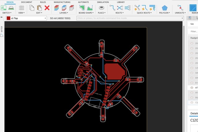
Designing the Sun LED Circuit
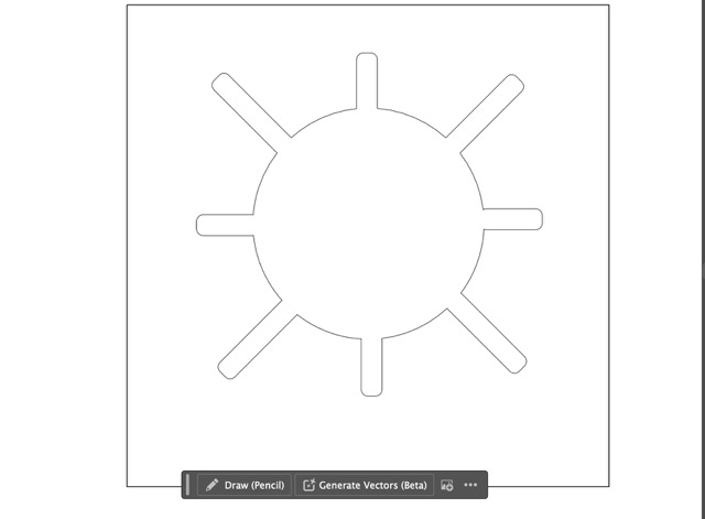
After gaining confidence from the tutorial, I decided to create my own custom design: a sun-shaped LED circuit. The concept is to have LEDs that can eventually light up with capacitive touch activation. I started by designing the sun artwork in Illustrator.
Design Concept
- Shape: Custom sun design with rays
- Controller: Xiao RP2040 microcontroller
- LEDs: Multiple LEDs positioned strategically on the sun
- Future Feature: Capacitive touch sensor to activate the LEDs
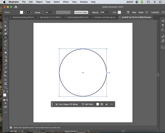
From Illustrator to Fusion 360
Creating a custom PCB shape required importing my Illustrator design into Fusion 360. I drew the sun shape in Illustrator, exported the outlines, and then imported them into Fusion Electronics to use as the board outline.
Workflow: Vector to PCB
- Illustrator: Drew the sun design with clean outlines
- Export: Exported as vector outlines (DXF format)
- Fusion Import: Imported the outline into Fusion 360 Electronics
- Board Outline: Used the imported shape to define the PCB boundary
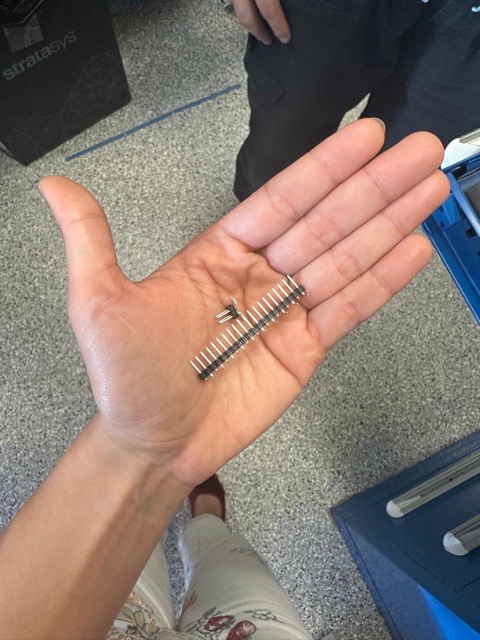
Visual Connection: Understanding the Layout
Having physical reference images was incredibly helpful in understanding how components connect and where traces should go. Being able to physically see the pieces and their relationships made the abstract EDA work much more concrete. Thanks to Anthony for showing me these visual aids - it completely transformed my understanding!

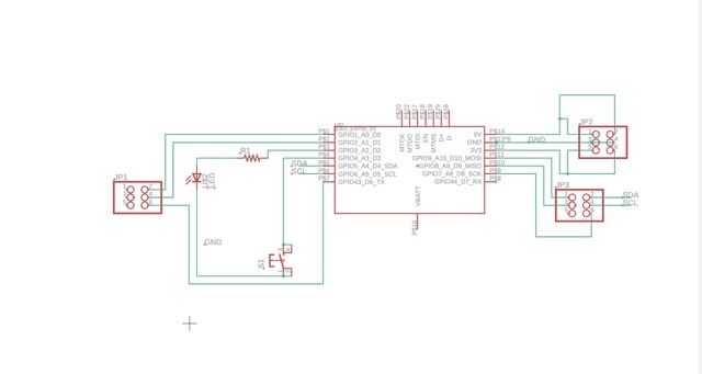
Creating the Schematic
With my board shape ready, I moved on to creating the schematic. This involved placing the Xiao RP2040, LEDs, resistors, and planning the connections for the capacitive touch feature (to be developed later). The Xiao RP2040 datasheet was crucial in helping me figure out what connects to where and understanding the pin configurations.


Components Used
- Microcontroller: Xiao RP2040 for control and future touch sensing
- LEDs: Multiple LEDs positioned around the sun design
- Resistors: Current-limiting resistors for each LED
- Touch Pads: Space reserved for capacitive touch implementation
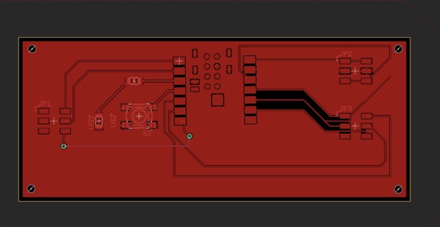
PCB Layout & Routing: Schematic → PCB Design
Moving from schematic to PCB design was the most challenging part. I had to place all the components within my custom sun shape and route all the traces. This is where things got TEDIOUS. TEDIOUS. TEDIOUS.
The Routing Process
- Component Placement: Positioned the Xiao RP2040 at the center of the sun, with some space for the USB connection to be instered.
- LED Positioning: Arranged LEDs around the sun rays for visual effect
- Trace Routing: Connected each LED to the microcontroller (manually, one by one)
- Power & Ground: Created power distribution network across the board
The Tedious Reality: Made a Mess, Hope It Works
Let's be honest — this process was incredibly tedious. Routing traces around a custom shape with multiple LEDs, making sure nothing overlaps, keeping track of all the connections... I definitely made a mess along the way. The design rules kept yelling at me about clearances and trace widths. But hopefully, when I eventually fabricate this, it actually works!

Challenges Faced
- Custom Shape Constraints: The sun outline limited where I could place components
- Trace Congestion: Too many connections in too little space
- Design Rule Violations: Constantly adjusting to meet minimum clearances
- Time Consuming: Manual routing took much longer than expected
- Learning Curve: First time doing a complex custom-shaped PCB
Lessons Learned
Despite the tedious nature of the work and the messy process, I learned a tremendous amount this week. Electronics design automation is not just about clicking buttons — it's about understanding the constraints of manufacturing, the physics of circuits, and having patience (lots of patience) for the routing process.
Key Takeaways
- Custom Shapes Are Hard: Working with non-rectangular PCBs adds significant complexity
- Fusion 360 Electronics: Powerful but requires patience and practice
- Start Simple: Following a tutorial before experimenting on my own was essential
- Xiao RP2040: Great microcontroller choice for small, custom PCB projects
- Iteration is Key: First designs are never perfect — and that's okay
- Hope for the Best: Sometimes you make a mess and just hope it works when fabricated!
Next Steps
The next phase will be fabricating this sun LED board and testing if it actually works. I also plan to develop the capacitive touch feature so the LEDs light up when touched. Stay tuned to see if my messy design becomes a functional circuit!
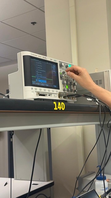
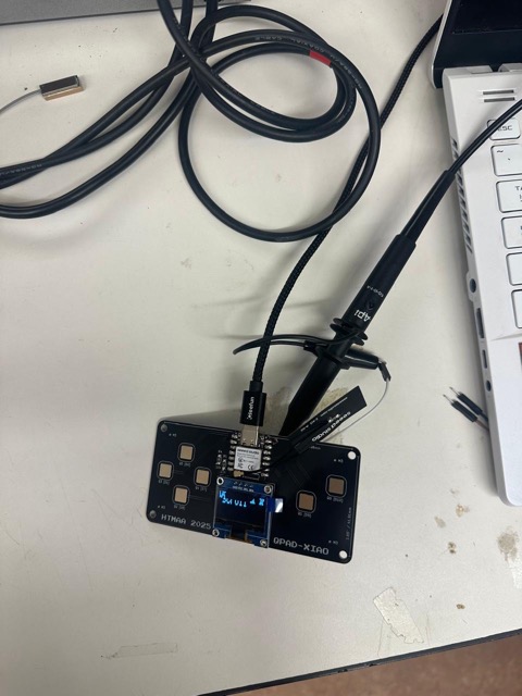
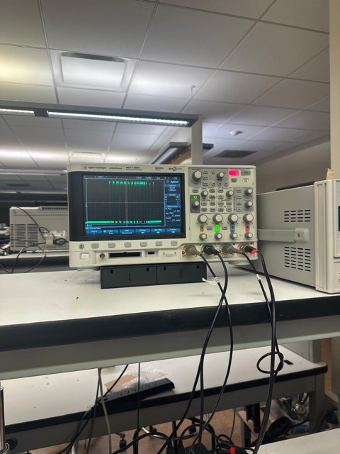
Group Assignment: Electronics Testing & Measurement
This week's group assignment focused on understanding the essential tools for testing and debugging electronics: multimeters, oscilloscopes, and logic analyzers. These tools are crucial for ensuring board safety and diagnosing issues. View full group assignment documentation.
Multimeter: The First Line of Defense
The multimeter is the first piece of equipment you should use when testing any board. It measures voltages (3× per second), resistances, and current. Most crucially, it tells you if your board is safe to plug into your computer.
Key Multimeter Tests
- Continuity Test: Under 50 ohms indicates continuity
- Voltage Measurement: Verify power rails before connecting
- Safety Check: Any board you make should be tested with a multimeter before plugging into a computer
- Resistance Measurement: Check for shorts between power and ground
Oscilloscope: Seeing Signals in Real-Time
For things that vary quickly, the oscilloscope can tell you things that nothing else can. Unlike the multimeter, the oscilloscope's probe clips to ground and measures signals in real-time.
What We Tested:
- Power Noise: 3.3V line showed ~300 millivolt noise range
- Digital Signals: Decoded serial communication by probing the transmit pin (pin 7)
- Debugging: Limited debugging to specific areas that weren't working
- ASCII Decoding: 8 bits (1s and 0s) can make up all letters (see ASCII table)
Communication Protocols
TX/RX & Baud Rate: Serial communication requires matching transmit (TX) and receive (RX) pins with the correct baud rate.
I²C Protocol: Uses two lines - SDA (data) and SCL (clock). The clock line can be measured as a consistent 101010101 pattern. The wave morphology carries the most interesting information to analyze.
SPI vs I²C: Different communication protocols require different measurement approaches.
Logic Analyzers: Making Sense of Digital Data
Logic analyzers condense and make more sense of complex digital signals. They're particularly useful for debugging communication protocols where you need to see multiple signals at once and decode their timing relationships.
Key Takeaways:
- Always Start with Multimeter: Safety first - check your board before powering
- Oscilloscope for Debugging: Essential for seeing what's actually happening on signal lines
- Understand Protocols: Know your communication protocols (I²C, SPI, UART) to debug effectively
- Wave Morphology Matters: The shape of signals tells you about signal integrity and timing
Sources
- Anthony's Fusion 360 Electronics Design Tutorial
- HTMAA recitations and EDA lectures
- Group Assignment: Testing and Measurement Tools Workshop
- Fusion 360 Electronics documentation
- Xiao RP2040 datasheet and pinout diagrams
- Adobe Illustrator for custom PCB shape design
- ASCII table and serial communication protocols
Special Thanks
A huge thank you to Anthony for the excellent EDA tutorial and for showing me the physical connection references that made everything click. And to Quentin for the guidance and support throughout the electronics learning process. Your help was invaluable in bringing this sun PCB design from concept to reality!