/ / / / / / / / / / / / / / / / / / / / / / / / / / / / / / / / / / / / / / / / / / / / / / / / / / / / / / / / / / / / / / / / / / / / / / / / / / / / / / / / / / / / / / / / / / / / / / / / / / / /
week 06 / electronics design
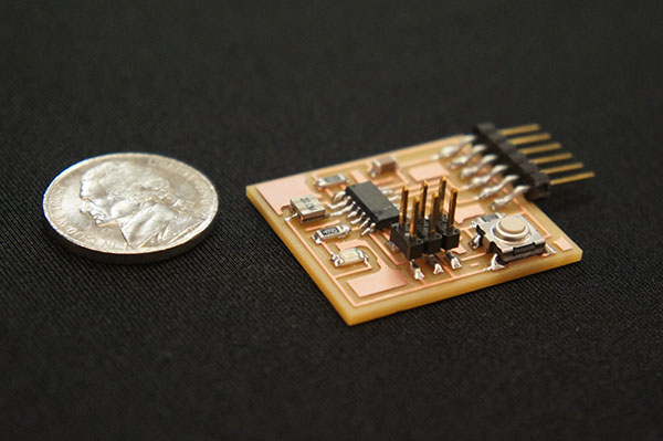
This assignment marked a return to electronics. Last time, we produced a circuit board for a microcontroller based on a schematic and instructions provided to us; this time, we have to not only produce a board but also create a digital layout from scratch, and alter its design by adding a couple of components. I created a board layout and modified the design of an "echo hello-world" board (I learned that "hello world" is a typical program for demonstrating a simple computer programming language to newbies like myself!).
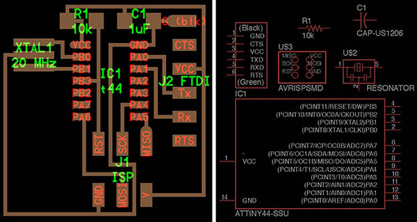
Starting from the original layout (left), I started a new schematic in the electronics design software Eagle (right), first by placing the known components onto the screen from the component library files provided for the class. A good tip in Eagle is to name the library files you'll be using once with a "01_" at the beginning, so that they're always at the top of the dialog box list when you initiate the "add component" command.
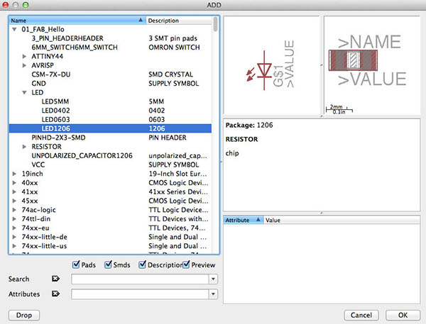
Next, I added two components, a button switch and an LED light, from the library.
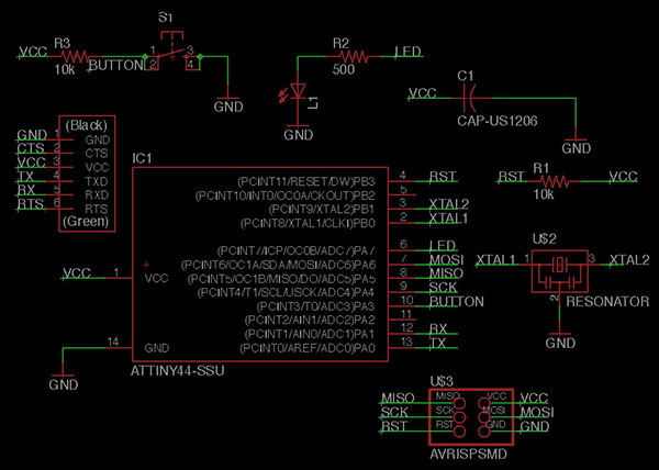
With all the components laid out in the schematic, the next step is to draw lines (using the "net" command) making connections between component pins. I learned from Rob, one of the TA's of the course, that when making a schematic in Eagle, it's not necessary to draw a full line connecting each pin; instead, I just draw a short line with a name and label that refers to its purpose (RST for reset, GND for ground, LED, etc). Any two nets that have the same name will be automatically connected behind the scenes in Eagle. Using this process, I made my connections, paying special attention to my two new components, the button and LED. The button requires a connection to ground, and a connection to power with a pull-up resistor before it. The LED requires a connection to ground preceded by a resistor to prevent burnout. (Some helpful info on resistors!)
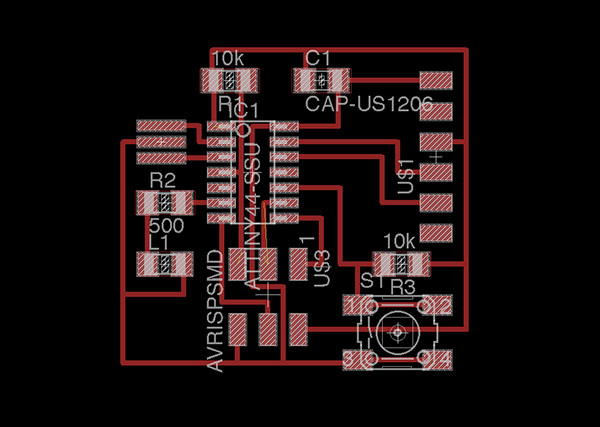
When the schematic is complete, I switch to board view in Eagle, and layout the location of my pads. I followed the Fab Academy tutorial for determining a functioning location for the button and LED, but there are a variety of ways to configure this. After setting up the board, I successfully ran Eagle's "Design Rules" check function to make sure my traces were spaced properly, for correct milling.
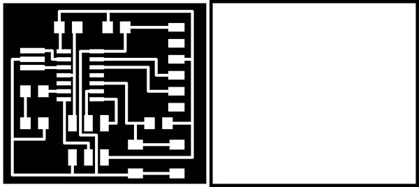
I exported a PNG image of the traces, and, in Photoshop, added 20px of white boarder around the image (make sure the colors are in the correct place! On the Modela, black is cut, white is left over). And then I saved a second PNG of just a 20px black border as my "cutout" file.
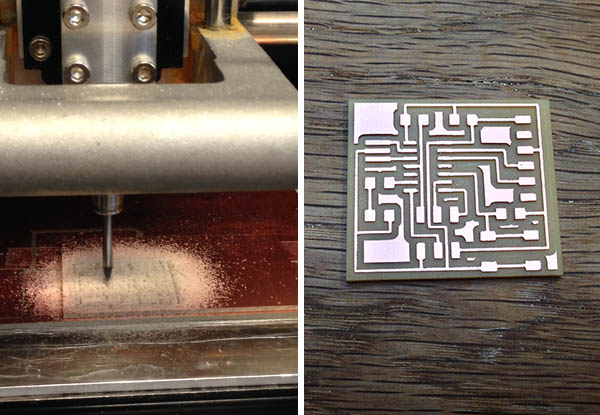
Now a pro at milling circuit boards on the Modela, I uploaded my PNG's to the fab module, made my toolpaths, and milled the traces and cut out the board.
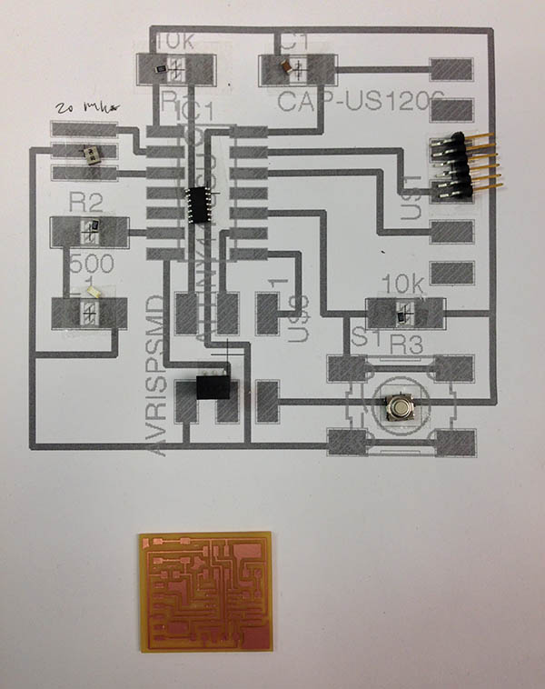
Transitioning to the "stuffing" phase, I printed out my Eagle board layout so that I could keep track of where the small components are to be placed on my board. And away I soldered...
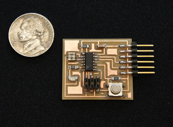
The board fully stuffed and cleaned. Ready to be programmed to turn on that LED light (and maybe other things?).
/ / / / / / / /
Files: