
Final Project: High voltage generator
Blocking Oscillator Circuit
I wanted to make a low-cost controllable high voltage generator from an input of 5V for my final project. I wanted to generate a maximum voltage of 3000V. Initially I thought that I could use a step-up transformer to generate high voltage. That's a lot of voltage to generate from 5V inputs. I figured out that I could use a blocking oscillator circuit and voltage ladder to achieve the voltage. I started to dig deeper into the these two circuits
Here's the basic blocking oscillator circuit: As Reece Pollack explains in his blog: "At the start of the cycle, current flows through the resistor R1, turning the transistor Q1 on causing current to begin to flow through the transformer winding L1. Since L1 is an inductor it impedes the change in current, and the current through L1 ramps up over time. In a transformer L1 and L2 are coupled, so the change in current in L1 induces a proportional change in current L2, charging capacitor C1. This supplements the current through the base of Q1, keeping it fully turned on. This is a positive feedback loop. This positive feedback continues until the transformer core saturates, after which there is no further change in current through L1. Since it's the change in current in L1 that induces a current in L2, and there is no longer a change in current in L1, the voltage across L2 drops. This causes C1 to discharge, drawing current away from the base of Q1 and turning it off. The current through L1 stops, and the change in current in L1 again induces a proportional change in the current in L2. Except this time the current flows in the opposite direction, pulling more current from the base of Q1 keeping it off until we reach the state we started in."
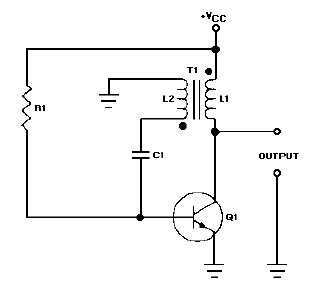
Here is the image source. Here are links I read to understand blocking oscillator circuit: 1 2 3 4
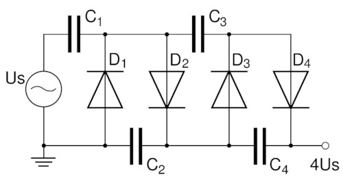
Voltage Ladder
A Voltage Multiplier is an electrical circuit that converts AC electrical power from a lower voltage to a higher DC voltage, typically using a network of capacitors and diodes. It allows the buildup of charge only in one direction and hence converts the AC signal to a DC.
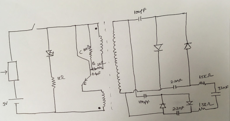
Blocking Oscillator + Voltage ladder
The following circuit is based on Trapro Bugzapper and the references. I took the basic circuit from the bug zapper and modified it accordingly.
Electronics design
Components used:
1. A Stepup transformer with two primary coils and one secondary coil
2. Two 100pF capacitors or above
3. Two 2.2nF capacitors or above
4. 4 Diodes of 2500mA/400V
5. Two FTDI headers
6. 6 safety resistors of 1Mohm
7. One 33nF/22nF capacitor
8. Two safety resistros of 15kohm
9. NPN transitor
10. 0.1uF capacitor
11. one Potentiometer of 10ohm and 5W
12. Red LED
13. 1k SMD resistor
14. 10k SMD resistor
15. 2x2 SMD header
16. Input microUSB
17. USB cable
18. Jumper wires
I designed my schematic and the board in Eagle.
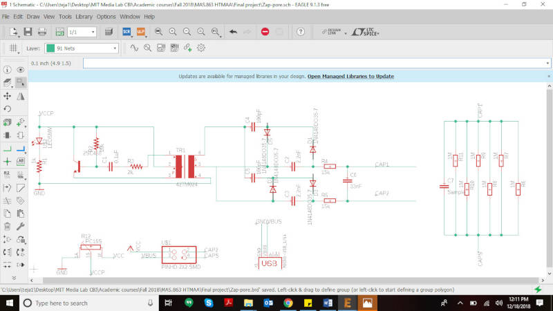
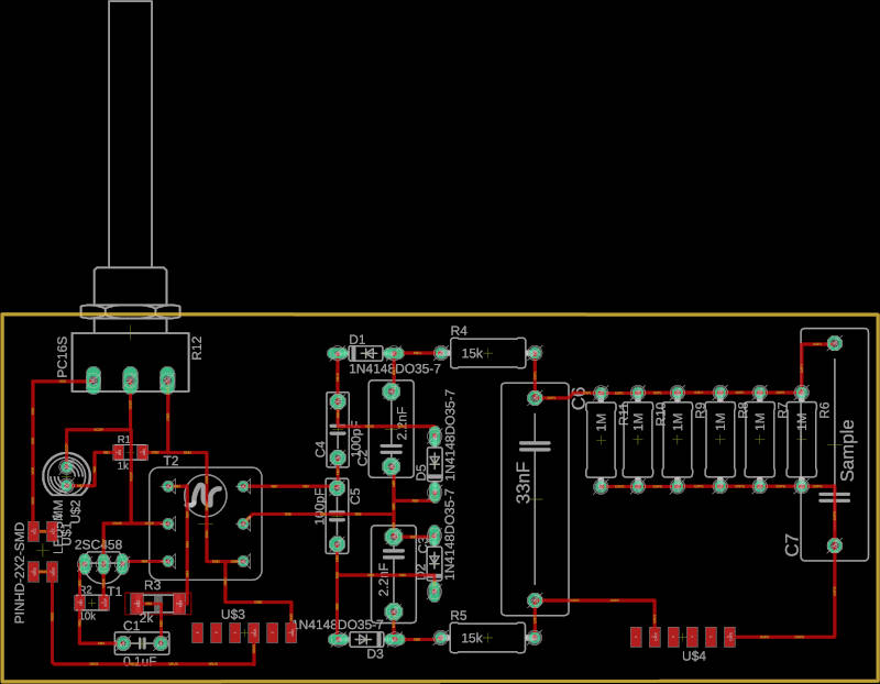
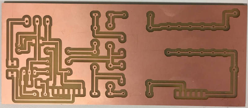
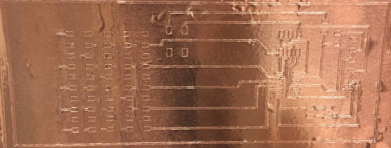
Here are the traces and outline generated from Eagle


I cut the PCB board using Roland MDX milling machine and mods software
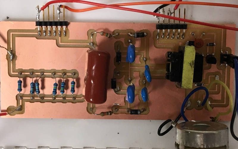
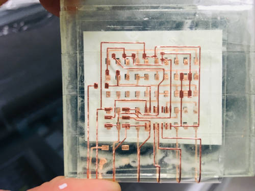
I soldered all the components. Powered the circuit using the USB. I found that the 33nF capacitor is not being charged at all. I started troubleshooting using a multimeter checking if the circuit is well connected or if there are shorts. I found out that the transfomer is not outputting any voltage. I figured out that the output pins of the transformer are not well soldered. When I tried to resolder them, the traces detached from the board. I remilled the board using the milling machine, and soldered the components again. This time it sparked because the traces are so close, it arced.
I remilled the board but this time I used offset command and made it from 4 to 8. This allowed me to distance traces from each other very well. This time it didn't arc! I could solder the components well!
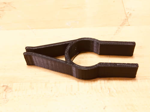
Using Additive manufacturing for DPDT switch
Inorder to switch on the circuit and discharge the capacitor, I made a DPDT Switch controlling both the circuits: When one is switched on, the other is off and vice versa. Here is the 3D printed file of the switch. My plan is to wrap copper tape around four movable parts of the switch and then solder them with wires.
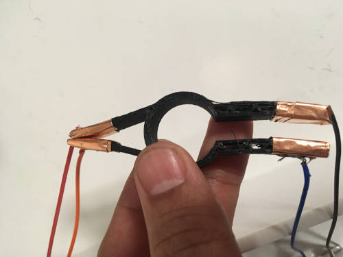
I could measure the high voltage using an oscilloscope. I used a 100x oscilloscope probe as I am measuring high voltage. I set the oscilloscope to use single channel and display 100x voltage as it can handle only 300v without probes. I could generate a maximum of 3000V with the board when the potentiometer is turned to it's maximum.
High voltage measurement
As I turn the potentiometer, I can control the output voltage from 100V to 3000v.
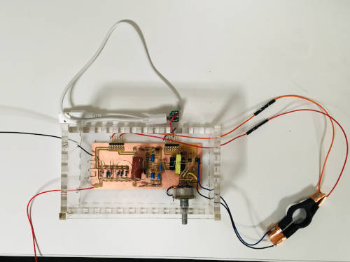
Electronics in the pressfitted box
I made a pressfit kit to keep the whole electrinics inside by allowing the user to interact with the potentiometer to control the input voltage, switch, powering the device with USB and output wires. After designing the CAD files in solidworks, I lasecut sheet acrylic of thickness 6mm and made the pressfit box.
1. I designed the base file first and then glued the electronic board to the base using a double sided tape.
2. I then designed each of the sides and the top based on the electronic board and making sure my outlets are good to fit the electronic components for the user interaction.
3. I realized that my sides weren't fitting the base well. I had to play with the width of zigzag pattern to make sure it fits. The zigzag pattern is designed to be 6mm for the base. The sides alternate between 5.75mm and 6.25mm.
Logo display with input and output devices
I wanted to make an LED display of my project logo with an input device [switch] and output device [LED]
I wanted to use vinyl cutter to make LED array board using a copper tape. I attached the copper tape to acetate layer and started vinyl cutting the traces with a speed of 20cm/sec and force of 80gf. I had a couple of failures but I finally made it. When I started to solder them after gluing the acetate layer to an acrylic, I realized that the whole board was twice the size of my traces .png file. One of the shoppers told me that it happens when you import .png into coreldraw. I had to redo the same process, but this time I used a .ai file and reduced the file size by 50% when I imported to coreldraw. This worked and the traces came out well. Once I am done with peeling the unnecessary parts of the copper tape. I soldered the components and made an LED array like this. I couldn't pour the epoxy on the traces as we ran out of epoxy.
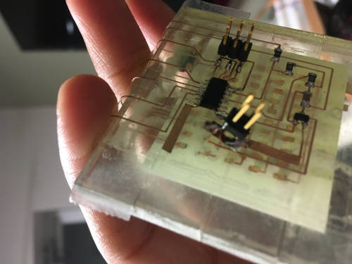
I started programming the board. There were no shorts or errors. I could program it well an the LED array was working. The ISP header and some of the traces detached from the acetate surface as I was moving the board. I tried to make traces on my own, but I couldn't do it. I then realized that epoxy is extremely important to keep the traces in tact.
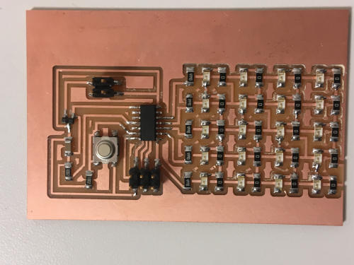
With the vinyl LED array failure, I tried to implement double layer LED array without zero resistors shown here, I milled the board and soldered the components and used a vinyl sticker to make it double layered. After I soldered the components and programmed it, I could see 6 of the LEDs lighting up but the rest not. I started trouble shooting, I realized that although the solders were good. The copper trace connecting different LEDS wasn't touching the pads below. I tried to redo the board, I had a similar failure.
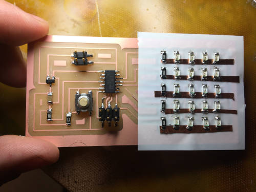
After a lot of failures, I finally decided to go with the board I made during output week to display my logo
Here is the integrated device