Week 2: Electronics Production
This week, I learned how to mill a PCB and then solder components on the PCB "properly". The process involves two steps: 1) Milling a copper board 2) Soldering the components. Towards the end of the assignment, I came to a conclusion that the solders I have done before were of very low quality. This assignment taught me how to make shiny solders without wasting excess of solder.
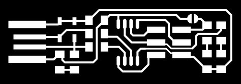
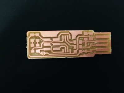
We used Roland Modela MDX-20 milling machine to cut the PCB and end-mill bits 1/64” for traces [which constitute the circuit], 1/32” for outline cut [periphery of PCB]. Given a cicuit in .png format with clear traces in white color and the rest of the board in black color like the image shown below]. Mods software created by Prof. Gershenfeld can direct the end-mill to cut the traces and outline of the prescibed format.
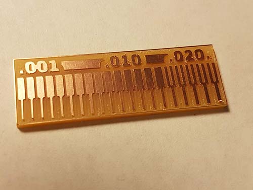
Group Assignment: characterize the design rules for your PCB production process
This is the result fo the characterization. We can infer that a gap width of .17 of an inch can be achieved and traces could be refined to 1 mil.
Individual Assignment: Make an in-circuit programmer by milling a PCB
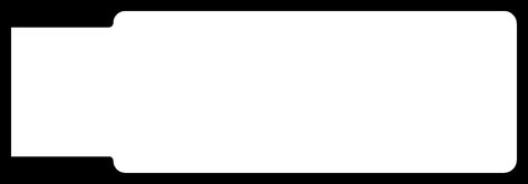
I used FR-1 copper board, 1x ATtiny45, 2x 1kΩ resistors, 2x 499Ω resistors, 2x 49Ω resistors, 2x 3.3v zener diodes, 1x red LED, 1x green LED, 1x 100nF capacitor, 1x 2x3 pin header, multimeter, solder station, double-sided tape to make this tinyISP. I referred to Max Allen's page for using mods software for PCB milling. The first time I cut the PCB, I chose a location which was near the edges. Once the traces and outline were cut, we could see in the following image that the traces were improper as some of the copper was uncut. I think this happened because the copper board was not flat enough at the edges to support a fine cut.
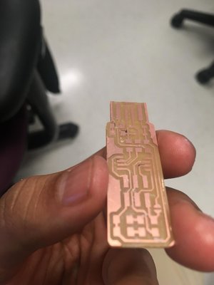
The second time I chose a flat location to cut the coper board, it came out fine.
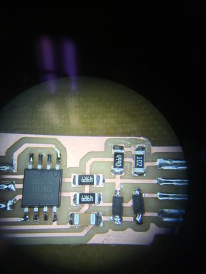
Once I have the milled PCB, I started soldering the components by fixing the milled PCB to the table using double sided tape. Using a microscope and tweezer, I could add components and then look through the microscope carefully while soldering. Thomas, who gave a wonderful tutorial on how to solder suggested four steps while soldering components such as resisors/capacitors. They are the following 1) We should heat up the copper trace first using the soldering tip and then place solder adjacent to the soldering tip without touching it, so that the solder melts and flows into the circuit board. The amount of solder should be very small. At this moment we don't introduce a resistor/capacitor 2) We place the resistor on the top of the solder on the trace and then heat up the trace using the soldering tip. This step makes the resisor stick to solder and it's immovable 3) We should solder the other end of resistor, here we can use a a significant amount of solder than we used previosuly 4) Finally, we will come to the first end and then add significant amount of solder to finish the job. Here is a sneak peek of the process through microscope
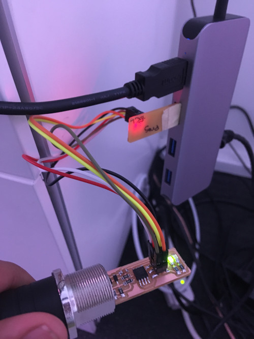
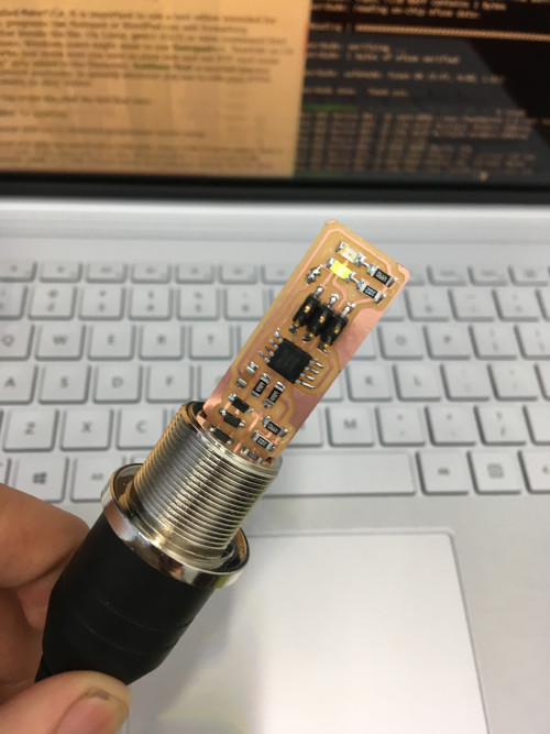
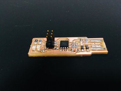
Once all component are soldered, the tinyISP looks like the following
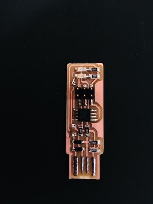
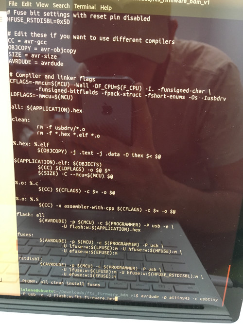
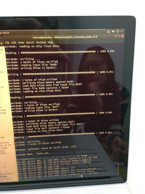
I used Elena's USP tiny as a programmer to make my USB tiny a programmer. I followed the steps in here. I had no errors in programming, mysoldering was fine!