Week 6
~ programming ~
This week on HTMAA, Hannah learns to program her Week 4 board so that the LED is controlled by the button.
More specifically, I want the LED to be on the on state while the button is pressed, and in the off state otherwise.
I began the week by looking through the ATTiny44 datasheet looking to figure out how to set the pins connected to the button and LED.
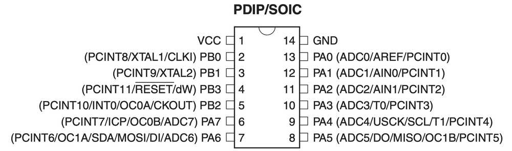
The most important thing about the device, for programming purposes, is going to be the pin diagram so that we know where to attach everything physically, as well as what the various pins are capable of doing:
The next thing that jumped out at me from the datasheet was the block diagram of all the internal components:
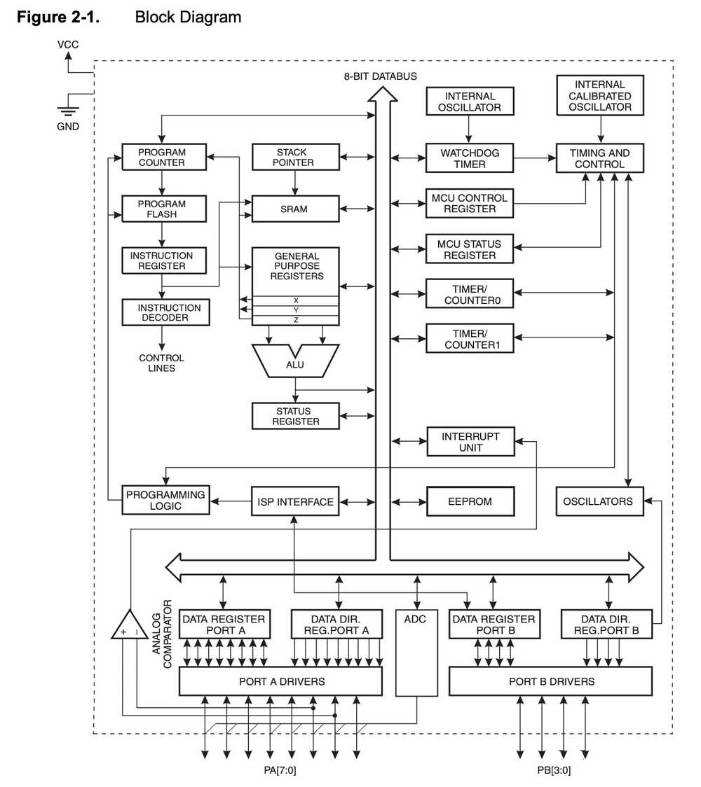
This AVR uses a Harvard architecture, that is separate memories and buses for program and data.
A note on memory:
EEPROM is flash like, i.e., it persists through power cycles. Fuse bits are similar. The program itself is stored on flash memory.
SRAM is erased during power off. SRAM is where calculations and variables my code runs will generally be stored here during use.
Fuse Bits
My experience with FPGA programming (6.111) has made me incredibly conscious about clock cycles, and in particular synchronizing logic to the rising edge of a clock. Here is the ATTiny’s clock setup:
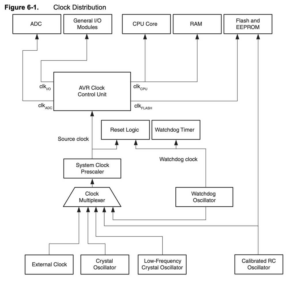
The week 4 PCB uses an external clock, so that will be what we want to select in the clock multiplexer. The code to select for each one is given as follows:
When we go to program the device, one of the commands we run in the make file is
program-usbtiny-fuses: $(PROJECT).hex
    avrdude -p t44 -P usb -c usbtiny -U lfuse:w:0x5E:m
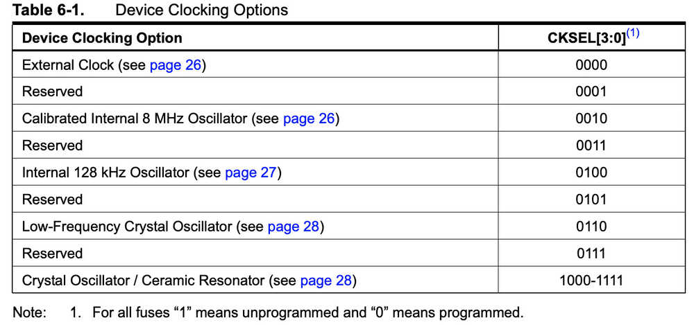
Note that lfuse is 0x5E which is 8’b01011110. What do these bits mean? We look in the fuse low table from the datasheet:

Matching our lfuse 0x5E=8’b01011110 bits means we have set CKSEL[3:0] = 1110, CKDIV8 = 0, CKOUT = 1 and SUT[1:0] = 01. Referring back to Table 6-1, we find that CKSEL[3:0] = 1110 means we are using a ceramic resonator. Which we are!
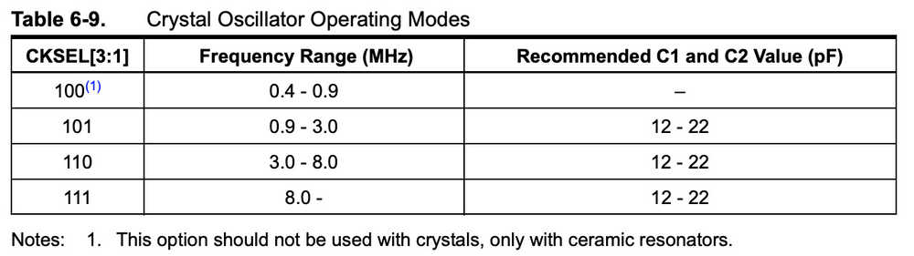
Table 6-9 tells us that the bits CKSEL[3:1] = 111 specify us using an 8.0 and up MHz clock. This is correct as our ceramic resonator provides a 20MHz oscillation.
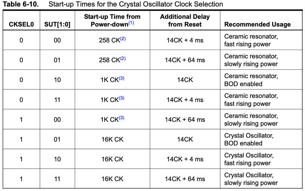
Table 6-10 says that our CKSEL[0] = 0 and SUT[1:0] = 01 specifies that we are in the ceramic resonator mode with the shortest delay from reset and shortest time from power-down.
Ok, what about this CKOUT = 1 bit? We find the datasheet on page 30 regarding the “Clock Output Buffer”
The device can output the system clock on the CKOUT pin. To enable the output, the CKOUT fuse has to be programmed. This mode is suitable when the chip clock is used to drive other circuits on the system. Note that the clock will not be output during reset and that the normal operation of the I/O pin will be overridden when the fuse is programmed. Any clock source, including the internal RC Oscillator, can be selected when the clock is output on CKOUT. If the System Clock Prescaler is used, it is the divided system clock that is output.
So what that means is that by enabling CKOUT = 1, we have sent the clock output to PB2, which is the ATTiny44’s clock output pin. Furthermore, this means we override use of PB2 as an I/O pin.
Finally, we examine the CKDIV8 = 0 bit. Page 32 of the datasheet says the following:
The CKDIV8 Fuse determines the initial value of the CLKPS bits. If CKDIV8 is unprogrammed, the CLKPS bits will be reset to “0000”. If CKDIV8 is programmed, CLKPS bits are reset to “0011”, giving a division factor of eight at start up. This feature should be used if the selected clock source has a higher frequency than the maximum frequency of the device at the present operating conditions. Note that any value can be written to the CLKPS bits regardless of the CKDIV8 Fuse setting. The Application software must ensure that a sufficient division factor is chosen if the selcted clock source has a higher frequency than the maximum frequency of the device at the present operating conditions. The device is shipped with the CKDIV8 Fuse programmed.
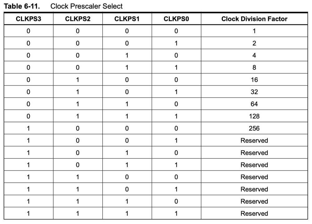
Ok, so given that CKDIV8 = 0 is its programmed state (which we learn by referring back to Table 19-5), then at startup, the clock will run at 1/8th the speed at startup. This makes sense since the ATTiny itself runs at a high speed of 8 MHz and our external oscillator is larger than that at 20 MHz. Thus, in line with the datasheet’s recommendation to use a clock scaling factor at startup if the external clock is faster than the internal one. Ok, so what about these CLKPS bits mentioned in the above paragraph?
Clock Bits
The CLKPS bits are in fact a familiar occurrence, as the following lines are the first lines of Neil’s code:
CLKPR = (1 << CLKPCE);
CLKPR = (0 << CLKPS3) | (0 << CLKPS2) | (0 << CLKPS1) | (0 << CLKPS0);

Section 6.5.2 explains further:
The CLKPCE bit must be written to logic one to enable change of the CLKPS bits. The CLKPCE bit is only updated when the other bits in CLKPR are simultaniosly written to zero. CLKPCE is cleared by hardware four cycles after it is written or when the CLKPS bits are written. Rewriting the CLKPCE bit within this time-out period does neither extend the time-out period, nor clear the CLKPCE bit.
So, the above lines of Neil’s code refer to setting the ability to change the clock division bits, and then setting the clock division factor to 1.
Input/Output Bits
The first step in writing this program is to figure out how to tell the ATTiny which pin is receiving data from the circuit (the button at PB2) and which pin writing data to the circuit (LED at PA7). Basically, the ATTiny has “A” pins and “B” pins, all of which can be configured as either input or output.
I found this explanation a bit confusing, so I read up on it in the MAKE: AVR Programming book (highly recommend!). They said the following:
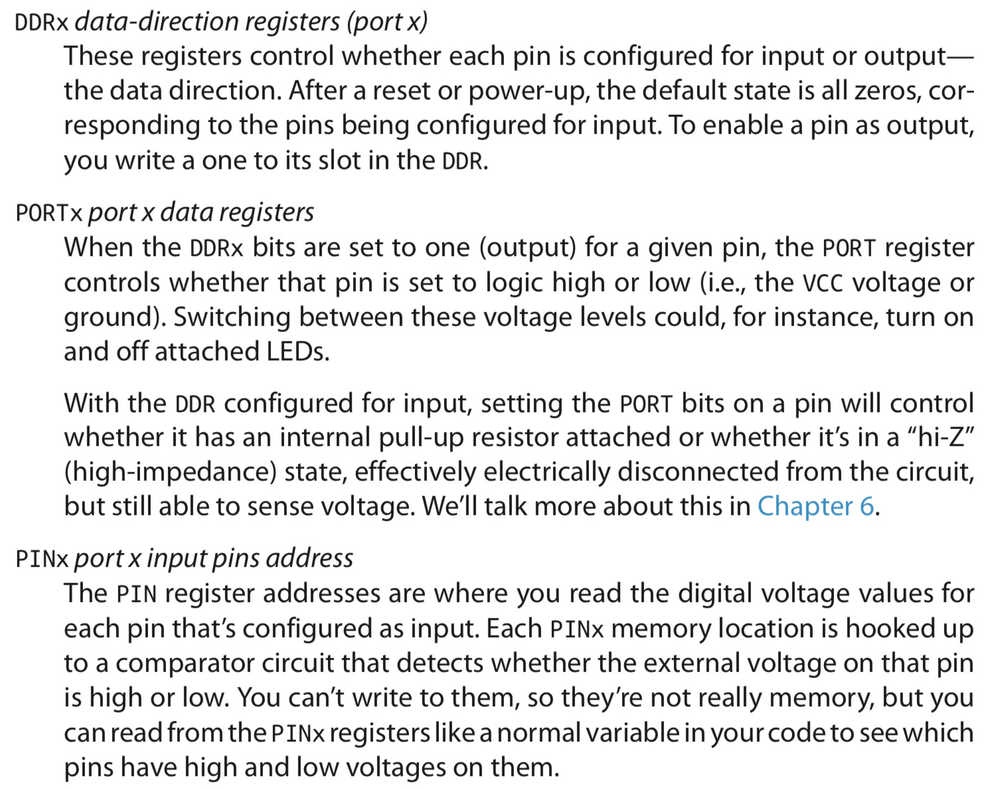
By default, all pins are input pins, so to output on a pin we must explicitly set its DDR (data direction register) to 1. Then for the individual pin we set it as HIGH or LOW by writing to the PORT register.
In c we may write 0x— for hex representation, 0b— for binary, and — for decimal.
So in summary:
output
DDRA = DDRA | (1 << led); #initialize led as output pin i.e. HIGH

PORTA = PORTA | (1 << led); # set led pin ON

PORTA = PORTA & ~(1 << led); # set led pin OFF
input
DDRB = DDRB & ~(1 << button); #initialize button as input pin i.e. LOW (default so this line is not needed)

PORTB = PORTB | (1 << button); %turn on pullup resistor if don't have one on board
Final Code
#include <avr/io.h>

//PB2 is input from button and PA7 is output for LED
#define led PA7
#define button PB2

int main(void){
    // set clock divider to /1
    CLKPR = (1 << CLKPCE);
    CLKPR = (0 << CLKPS3) | (0 << CLKPS2) | (0 << CLKPS1) | (0 << CLKPS0);

    // PB2 is input from button (default)

    // initialize PA7 as output for LED
    DDRA = DDRA | (1 << led);

    while (1) {
        //check if button is on
        if ( (PINB & (1 << button)) == (1 << button)) {
            PORTA = PORTA | (1 << led);
        } else { // turn LED off
            PORTA = PORTA & ~(1 << led);
        }
  }
}
