Designing a PCB
Exciting! always wanted to make my own PCB. This week task was to design our own “Echo Hello World” board, by mimicking an existing design and adding a LED and button to it. Obviously, it’s “How to Make” a.k.a the modern gladiator arena of creativity, so even though I don’t have any experience in this field, I thought to try and design the circuit to look like something. I have an animal theme going on in this class, but looking at the parts, I inevitably decided to go for a skull.
Design a schema
I chose to use Eagle, as Jake used it in the recitation and it seemed pretty straightforward and I could follow his steps. Also, the FabLab inventory library (relatively updated) as well as design rules file can be easily exported to Eagle.
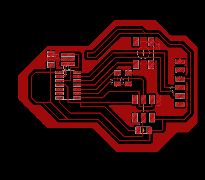
Starting with schematics, I started by following Neil’s design and then adding the button and the LED. I looked up at previous years “week 5” for some idea on what’s possible and what’s not, and arrived to the following schematic:
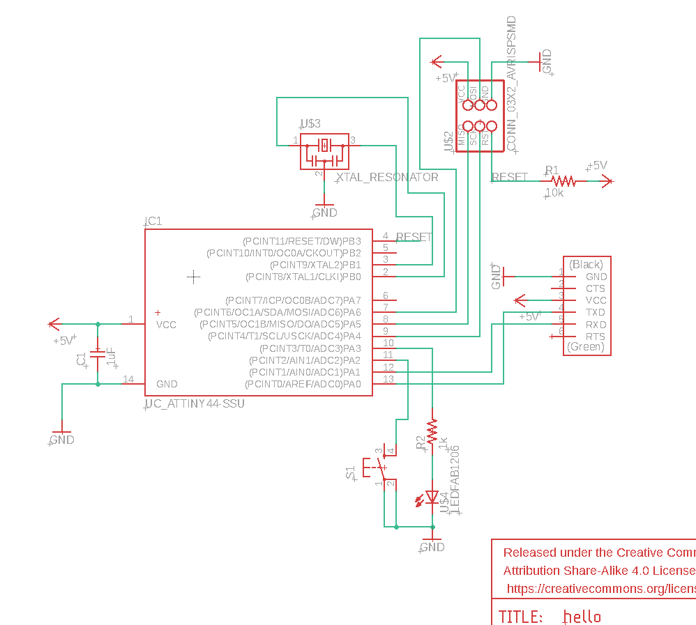
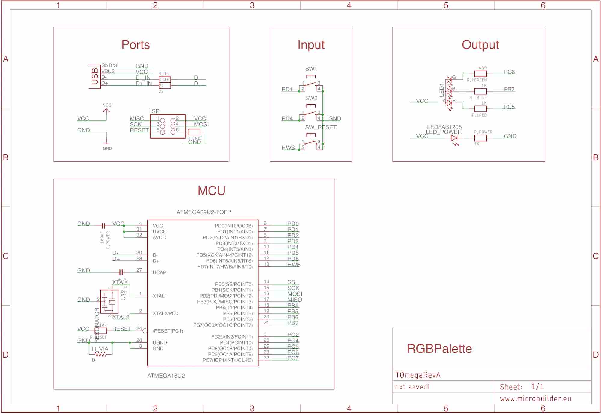
A few things to note. I know I can make it much more organized by labeling nets. I did it for RESET but except that I decided it’s not worth the effort for now. But I really like schematics which separates the parts logically, e.g. this board by Tomás.
Design a board
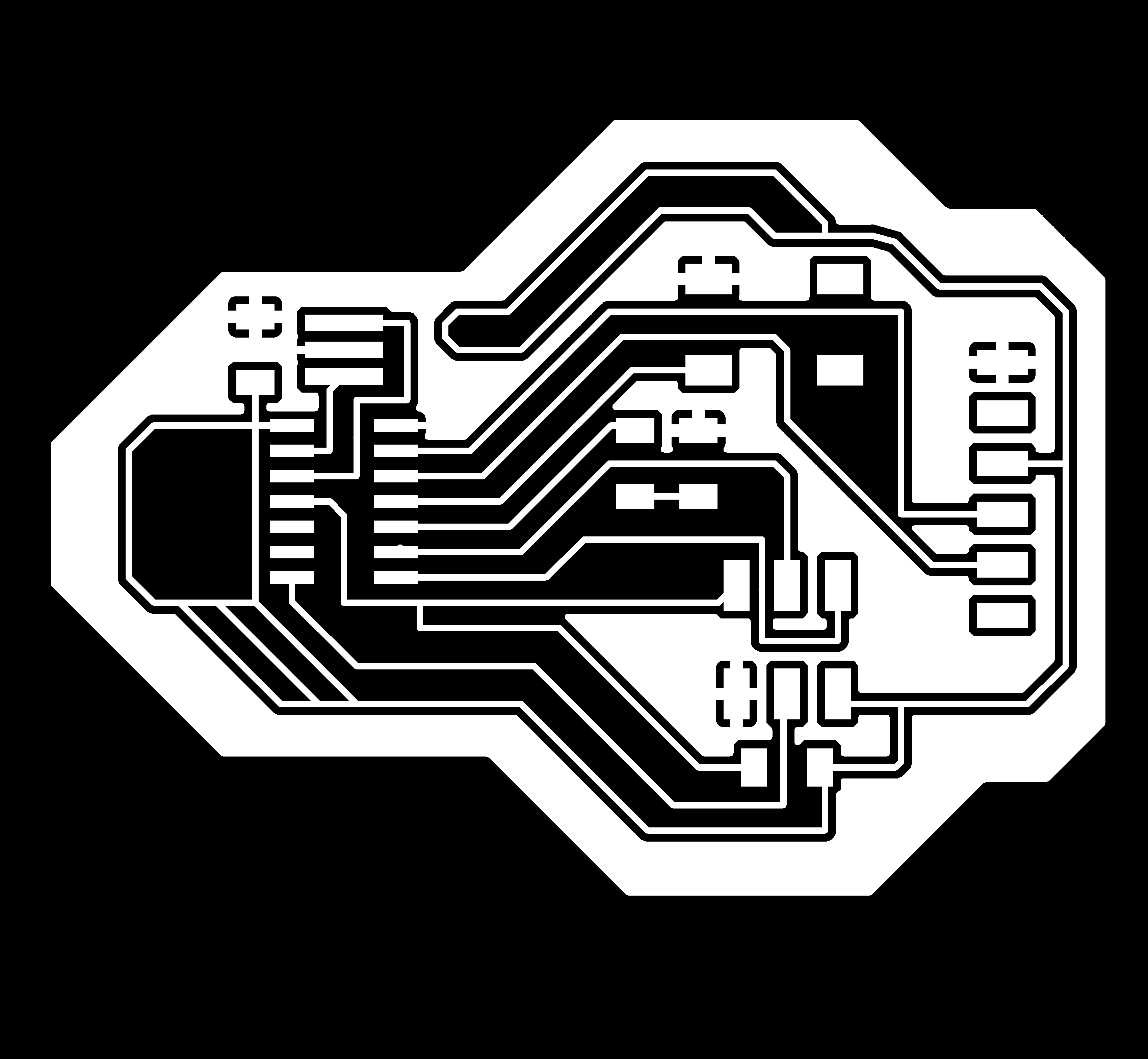
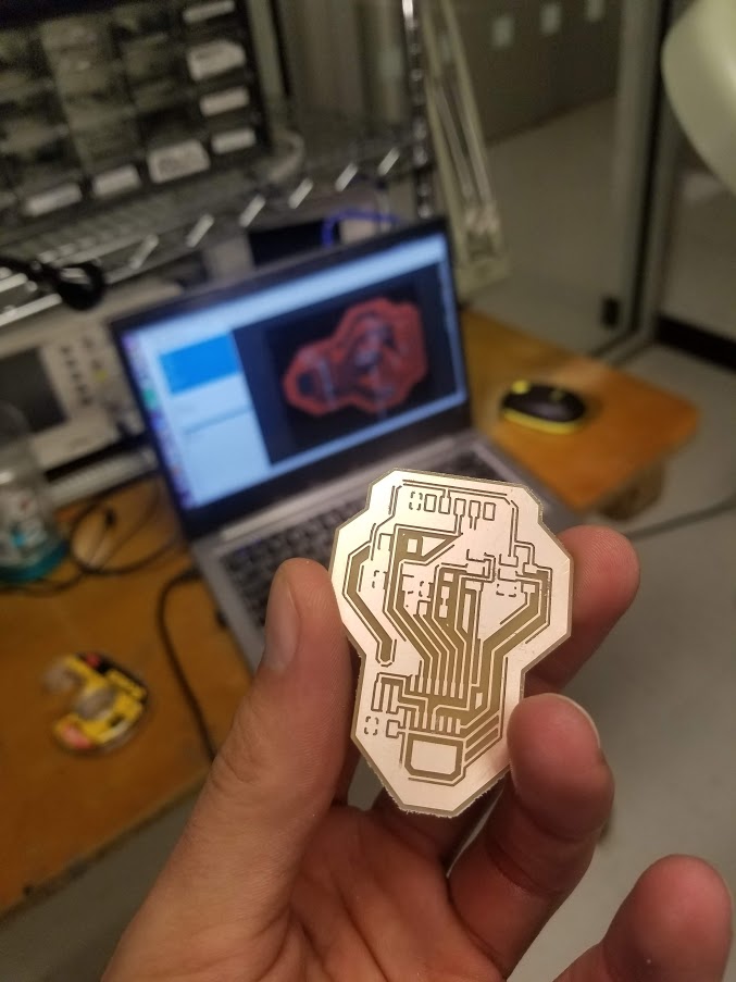
Next, moving on to design the board itself. As noted above, I decided to go for a skull shaped board, with the button as an eye, the microcontroller as teeth, and the FTDI header as a fashionable hairdo. This took a long time, but was weirdly enjoyable. Very similar to a puzzle game. I decided to use the GND trick Jake showed us - to fill the entire board as a polygon. To do so, I connected all of the other routes, and then filled up the skull polygon (create polygon -> ratsnest), and then moved around routes and pieces.
To export to high quality PNGs, I tried to use eagle_png.py - but it didn’t work :/ I read the Python code, and eventually just manually typed the following commands into Eagle everytime I wanted to export:
ratsnest; write;
set palette black; window;
display none top vias pads;
export image 'hello.top.png' monochrome 1500;
display none milling;
export image 'hello.cutout.png' monochrome 1500;
And… voila:
Off to the milling machine!
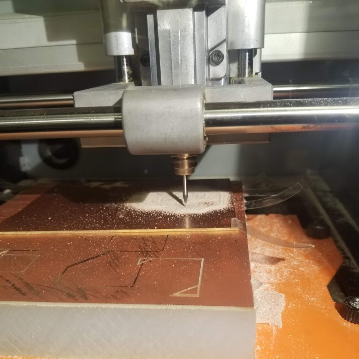
For the traces I used cut depth of 0.004in and max 0.008in deep (hence, double cut) and offset 4. At my first try, I put the origin too far, as apparently my board design was larger than I anticipated, so the end mill nearly “fell off”. I stopped it and reset it from a safer position. After a long while I get the result… and it was far from good :(
Might look nice at first, but check out all the flaws:
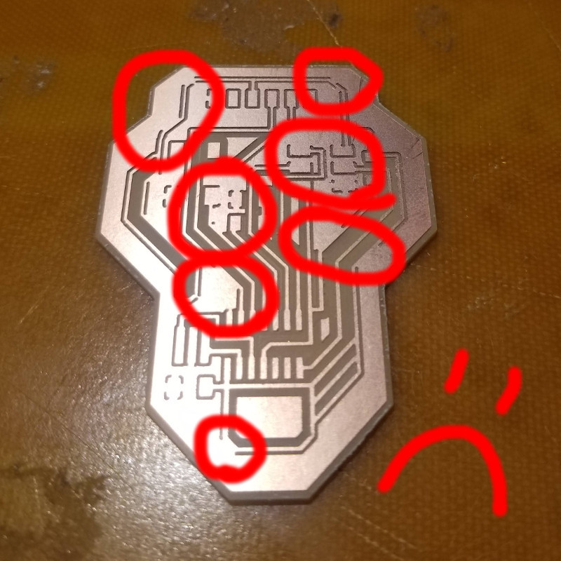
As much as I love flawed creations, I realized there’s no way this thing is going to work, and I can’t fix it with a razor and some manual work. My hypothesis was that the milling machine didn’t like all of the 45 degrees angles I used (you can see that most of the flaws are there) as well as the GND plane that is everywhere.
Design a board, Part II
Back to Eagle, I decided to give the same design another try, but using much “larger” design rules. Specifically, i figured that if 16mil works fine for straight routes, then 32mil should work fine for crooked ones. The process was enlarging a design rule, applying ratsnest, and solving the violations. One cool trick that really helped - using the button as a ground bridge! By rotating the button I could suddenly connect grounds in a much cleaner way. Eventually, I came up to this final design:
Here you can compare the old and new traces:
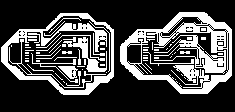
Pretty cool :)
Back to milling…
as it was after midnight I was pretty anxious to see the results… and it worked! However, there was something a bit weird, lots of little copper strings were still attached to the board. But after washing it, rubbing it and tweezing it - it looked good. Went to soldering in, and here is the result:
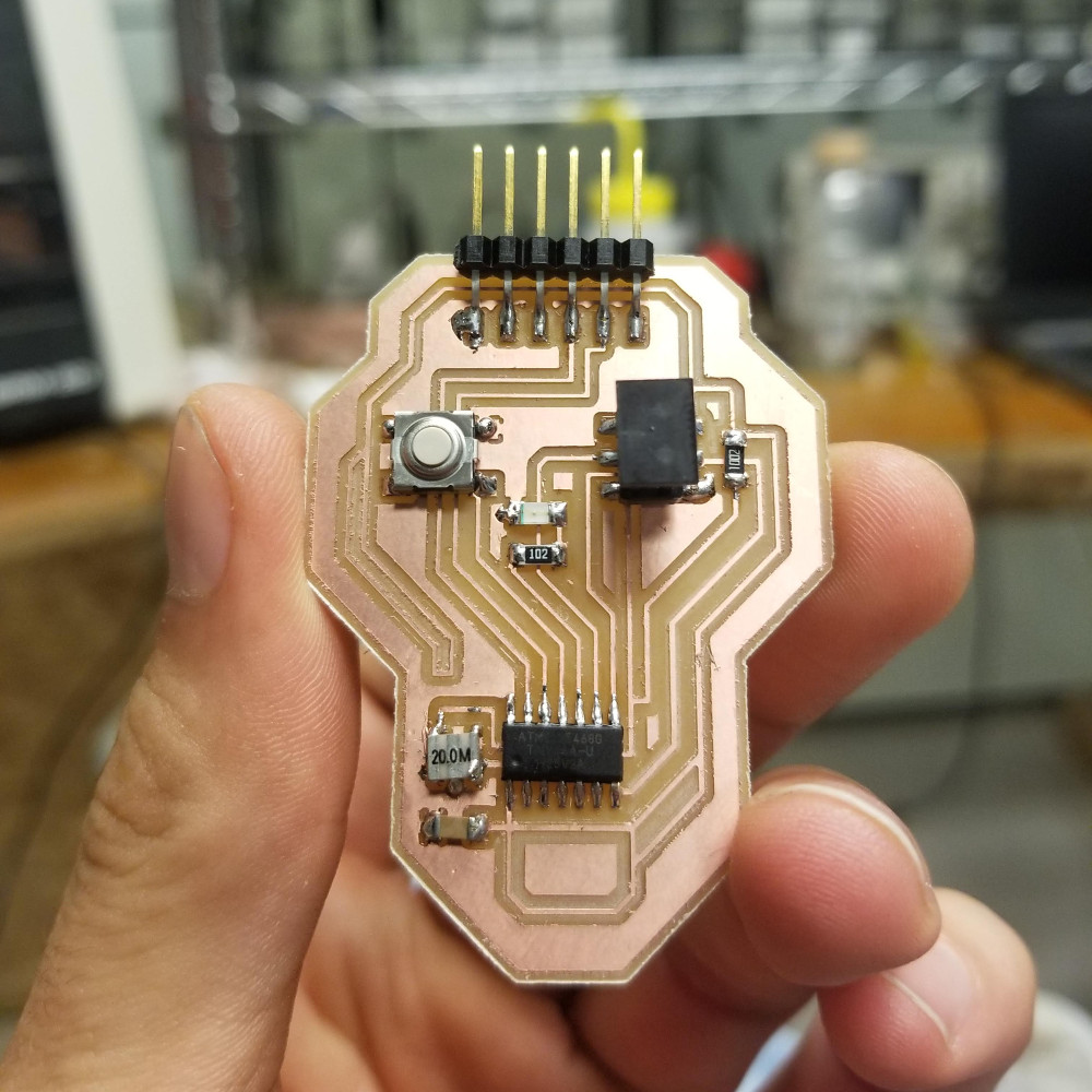
After careful examination, I was quite afraid that I soldered the resonator badly, as it seemed that it might be touching the ground plane next to it. Using the microscope, I saw the situation was not so bad and I cut out little copper strings that seemed “malignant”.
Programming
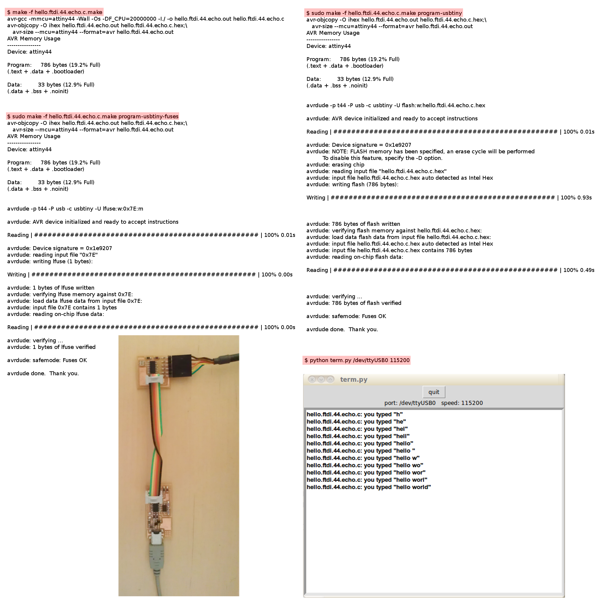
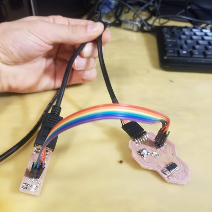
To program the board, I first tried to use my ISP from week 3. Connecting everything (not so easy to understand what goes where!) and following these instructions. The make, program-fuses and program commands all seemed to work fine… but I couldn’t get the last step to work. In the last step, I try to connect to my PCB to communicate by serial port. The Python script term.py didn’t work (tabs spaces issues, and then it seems my local pySerial was of a different version than the one written for it). Instead, I tried to just use a common Linux command to connect:
screen /dev/ttyUSB0 115200
Sadly, I kept getting [screen is terminating]. I thought maybe my programmer is broken, thus the board didn’t get programmed at all. I tried to use one of the stock programmers in the shop:

The first few commands (had to re-run using a different argument to fit with the programmer type) worked, but the screen kept on failing. Suddenly, I realized I should try to run it as root, and it worked!!
Oh the joy. I was still curious to see now if my programmer works or not. So I ran everything again, but used this opportunity to make a small change to the C code - I added a carriage return so the display on screen would look better.
put_char(&serial_port, serial_pin_out, '\"');
put_char(&serial_port, serial_pin_out, 13); // carriage return
put_char(&serial_port, serial_pin_out, 10); // new line
(lines 210-212)
Re-running everything using my own programmer:
And…
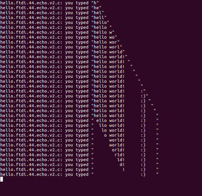
It works :)
The original design files for Eagle are available here and my modified C code is here.