This week was definitely supposed to be one of the most important weeks for me since, you know, the entire framework of my final project is based on a bunch of modules communicating using I²C. Did it work out that way? You'll have to stick around to find out.
Overzealous Board Design
I was stoked for this week. What better way to do that than to go all out? This was the first time I'd be able to focus on getting a bunch of hexagons to talk to each other! Before I got into that, there were some design hurdles I had to overcome:
- How am I going to sandwich two boards together?
- How big should I make the vias for the edges of the modules?
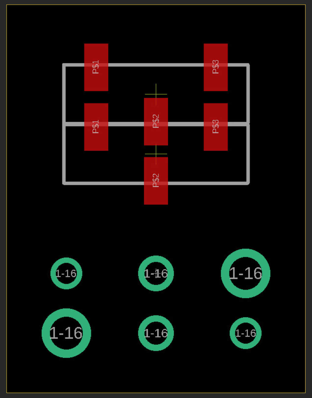
Alright, cool! What are those hole diameters? The smallest is a .9mm via, which is the same size as the rivets I'd been using. The middle one is a 1mm via, which would contain no rivet. I found some 1mm hole rivets in the shop, and "luckily" guessed that I should use a 1.4mm via diameter. (Yeah, this was wrong. The only reason it worked is because I milled holes into both sides of the board, and because it wasn't perfectly aligned, made the hole slightly wider than it should be. The correct via diameter is 1.5mm... Anthony warned me...)
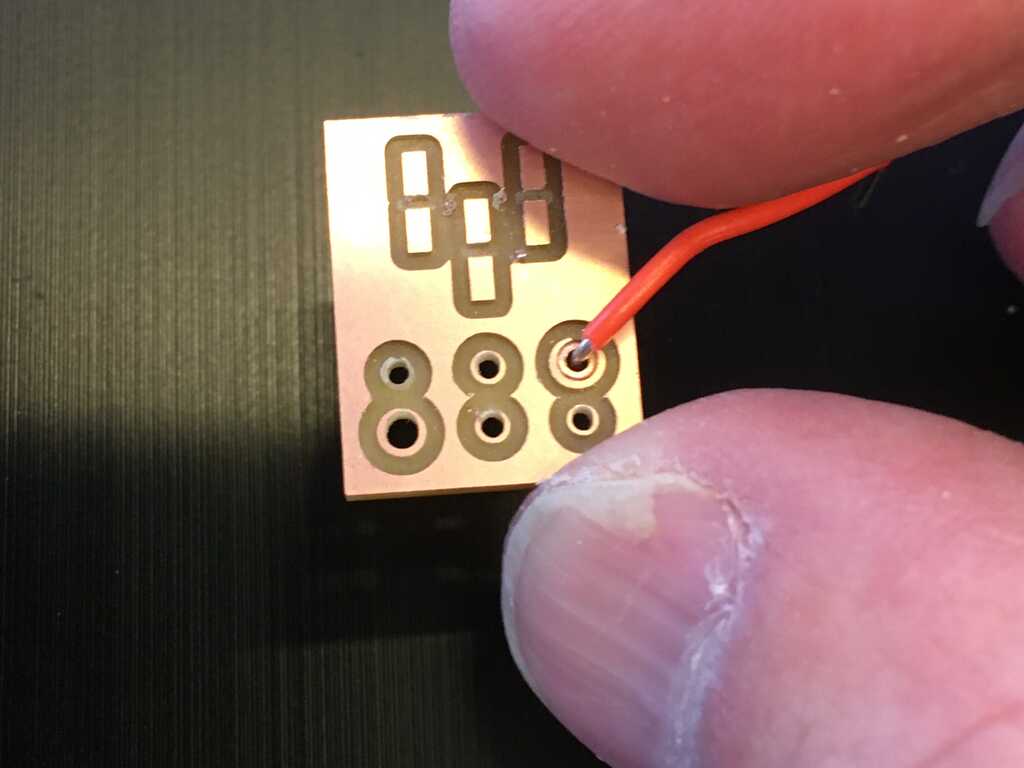
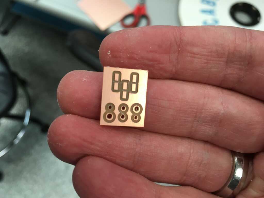
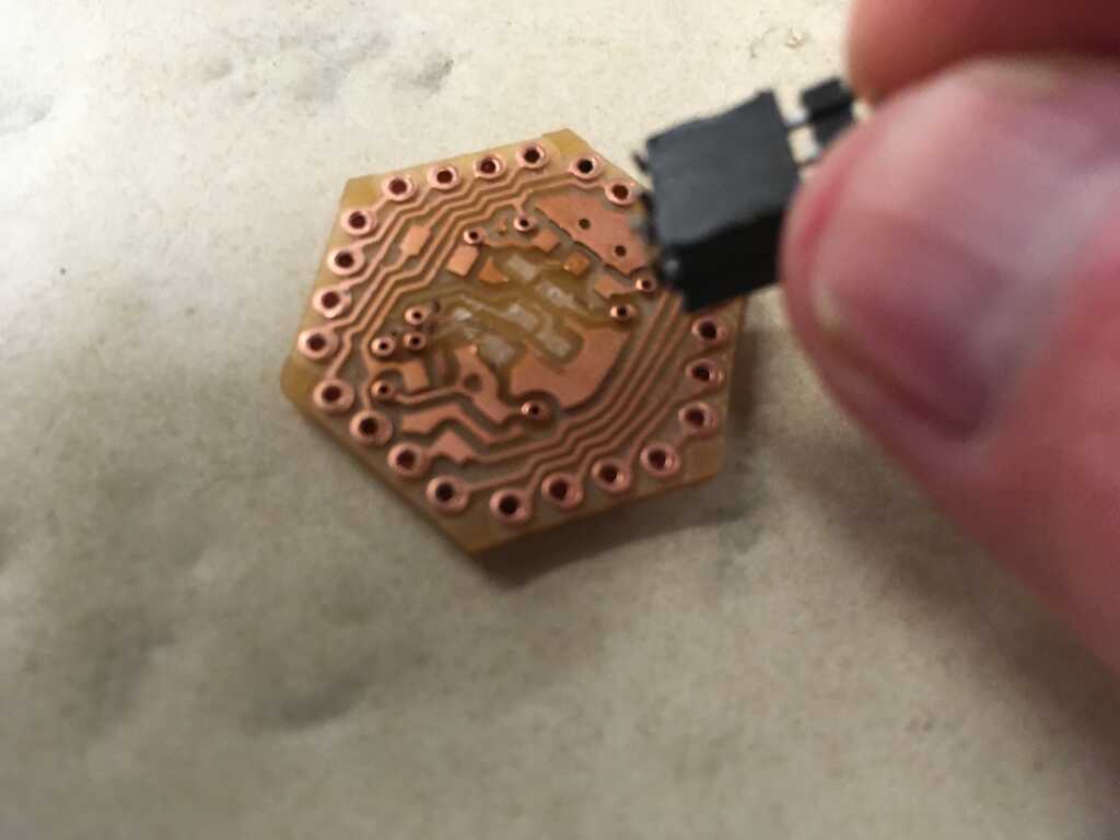
And the headers went on alright, too. (As you may notice, there isn't actually a way to test conductivity here... Not my greatest test board...)
Enough testing, let's get to the real stuff!
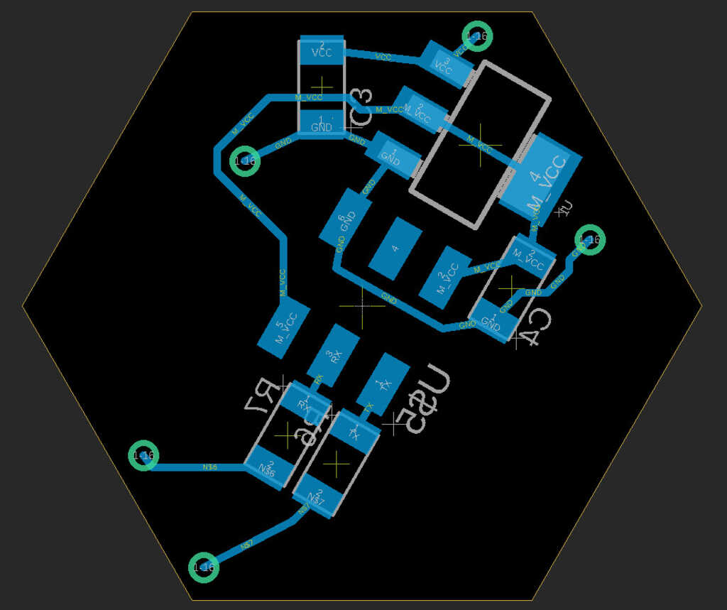
The Modules
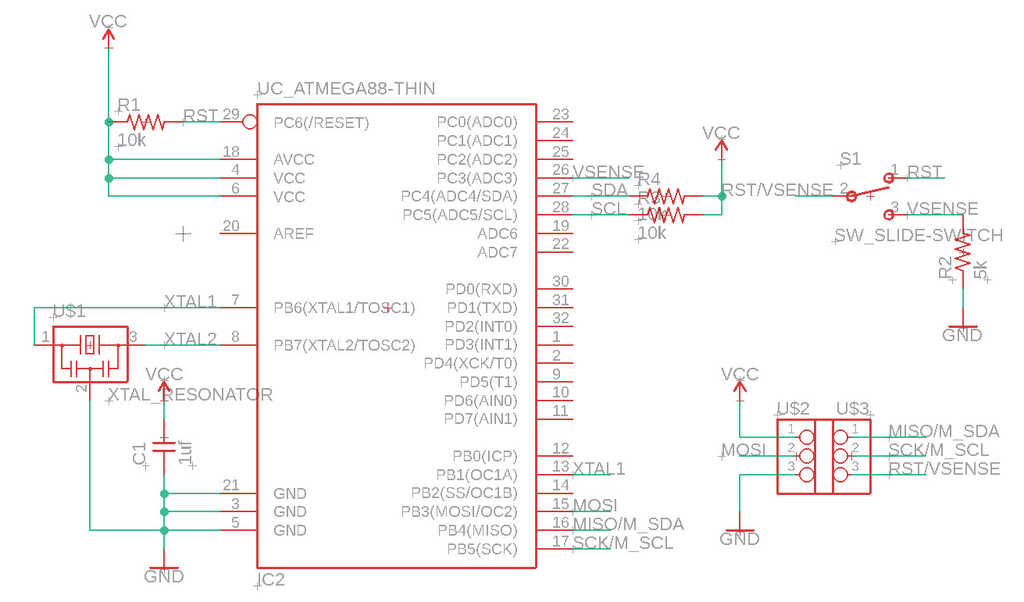
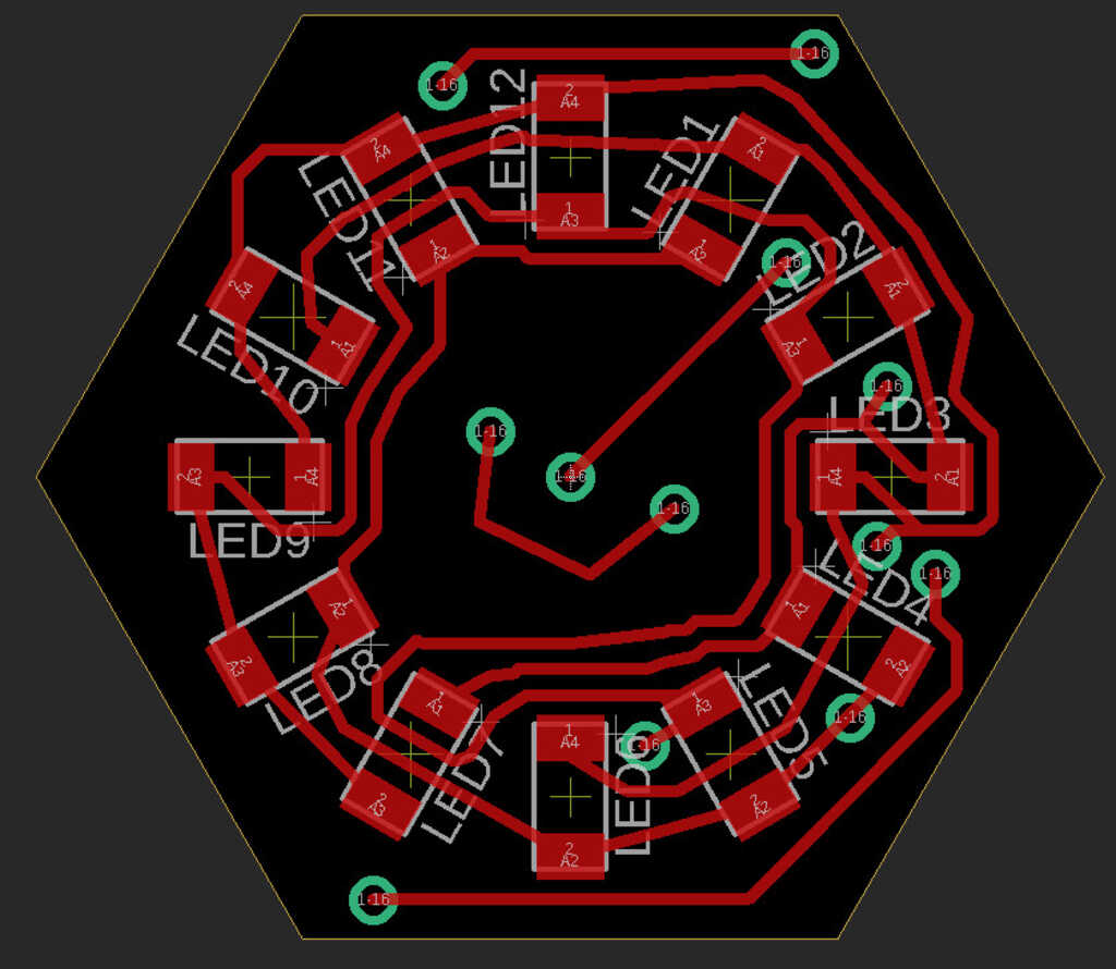
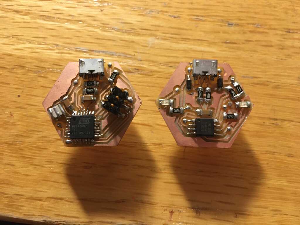
These are the bread and butter of the whole operation. They connect with each other in any direction, but orientation is important. I decided to run with an ATMega328P, ultimately because I only really "need" one hardware I²C bus for very fast inter-module communication. I can totally just bit-bang the peripherals. It's also useful since I can program it using ISP.
To communicate with the peripherals, there are now 6 pins. Most will only need 5 (power, ground, SCL, SDA, vSense), but this opens up the availability to SPI interfaces as well (5 pins + vSense). Most importantly, this allows for a programming peripheral. To program, vSense is no longer required, but access to the reset pin is instead. So, here, the switch swaps the reset/vSense pin on the header between the microcontroller's reset and GPIO pins.
Another important feature is pullup resistors for the I²C network. They're only necessary once along the entire line, so only one module will need them applied. The rest can leave it as an open circuit. By doing it this way, there's no need to mill two boards.
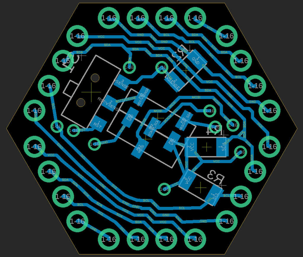
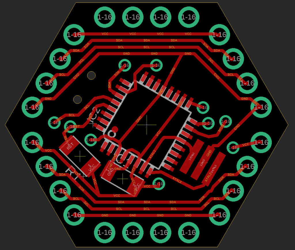
The design you currently see is slightly larger and has correct, 1.5mm diameter holes. I didn't get a chance to mill this, but this is the last version I had.
Note that the pins on the bottom header are mirrored so that it can interface directly with a peripheral.
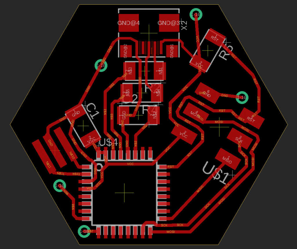
The Programmer
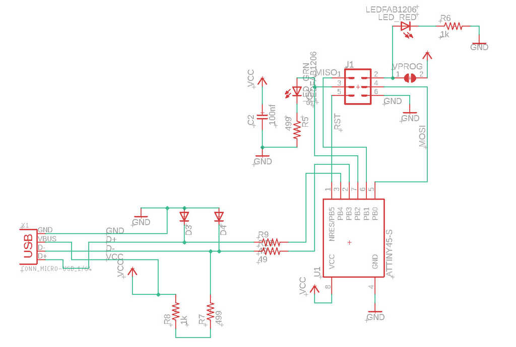
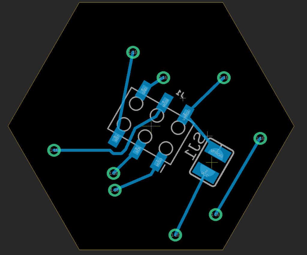
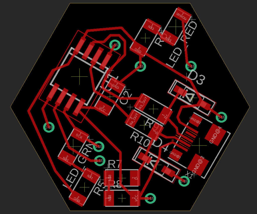
This is virtually the same as the programmer from Week 3, but I added the LEDs back in (they're incredibly helpful for debugging). It's just another fresh form factor, including a USB Micro port.
The FTDI
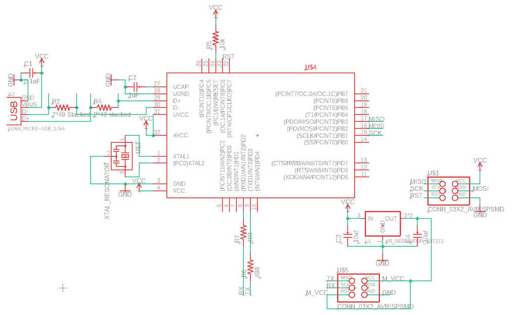
This is the same hardware as this great example, but also with a fresh form factor and USB Micro.
The Display
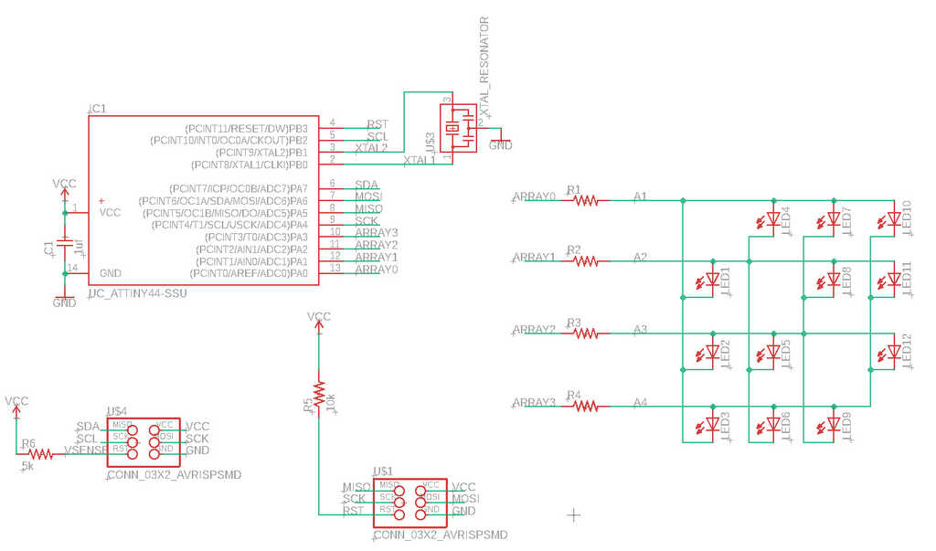
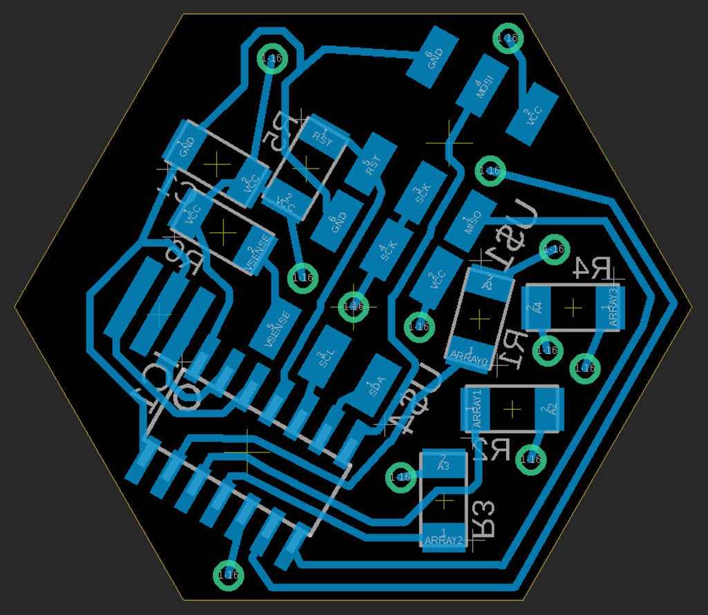
Almost the same as Week 10, but I rearranged some things. Now, instead of FTDI, it will communicate with a module via the central header. The programming header is now vertical; there should be enough clearance for it to fit. The other change is that I completely cleared off the top except for the LEDs to keep it clean.
Overzealous Milling
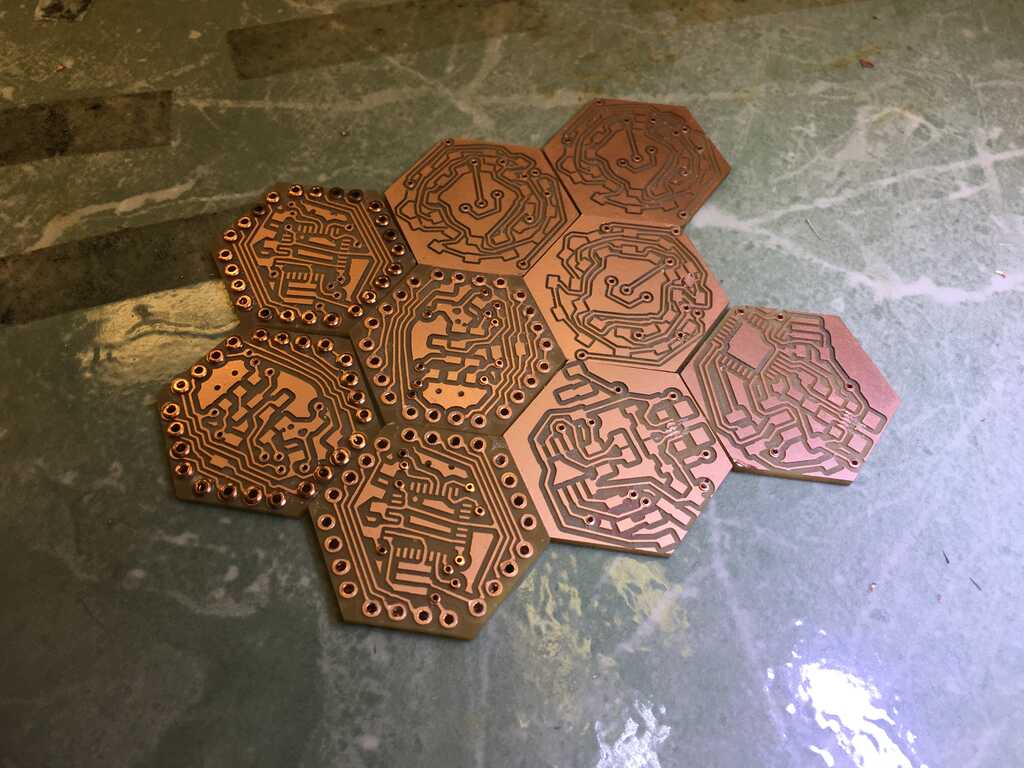
Wow. I underestimated how long milling all of this would take. It took up many, many hours just to get these things cut out.
To start, I did a test run. Lo and behold, one of the 1/64 end mills sucked and tore up the board:
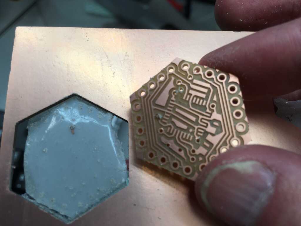
With a fresh end mill, it was buttery smooth. The next step was to figure out how to efficiently mill all of these boards. The best tactic I found was to place all of the boards in the software. Next, mill all of the traces (using "Mill All Visible" on the Othermill) with a 1/64th end mill (it ended up saving time, surprisingly). I chose to do the holes on this side as well. Doing so you just select "Holes" and run it with a 1/32nd end mill. However, I had issues with the end mill getting tape gunked all over it, which meant it would pull up traces around the hole. Yikes! So instead I would run one board at a time, and then wipe off the end mill. Phew! Flip, repeat the trace mill, and then run the outlines to completion. And...
Ah, so satisfying. The USB Micro traces were too small to be cut with the 1/64th, so I sliced them with precision knife.
Overzealous Riveting
What's not so satisfying is realizing I had to fill all of those holes with rivets. That alone took ages. What I wasn't prepared for, though, was my 1.4mm holes not fitting the 1.5mm diameter rivets... This was only Friday, and I knew I didn't have enough time to spend another day remilling the boards. I needed progress. So I stuffed them in anyways.
Yeah. Also not one of my best ideas.
At least they looked pretty?
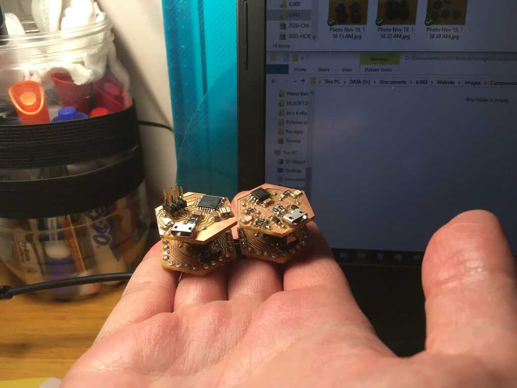
Not-So-Overzealous Stuffing and Programming
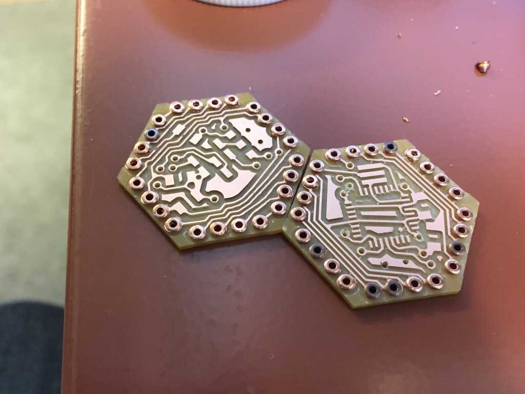
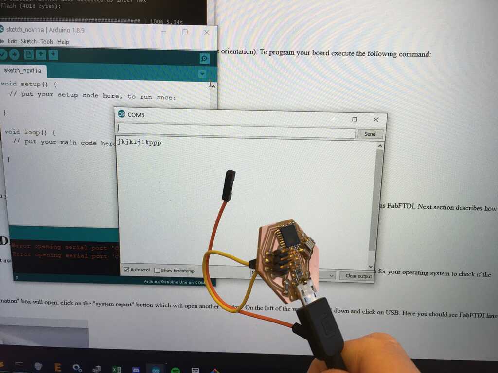
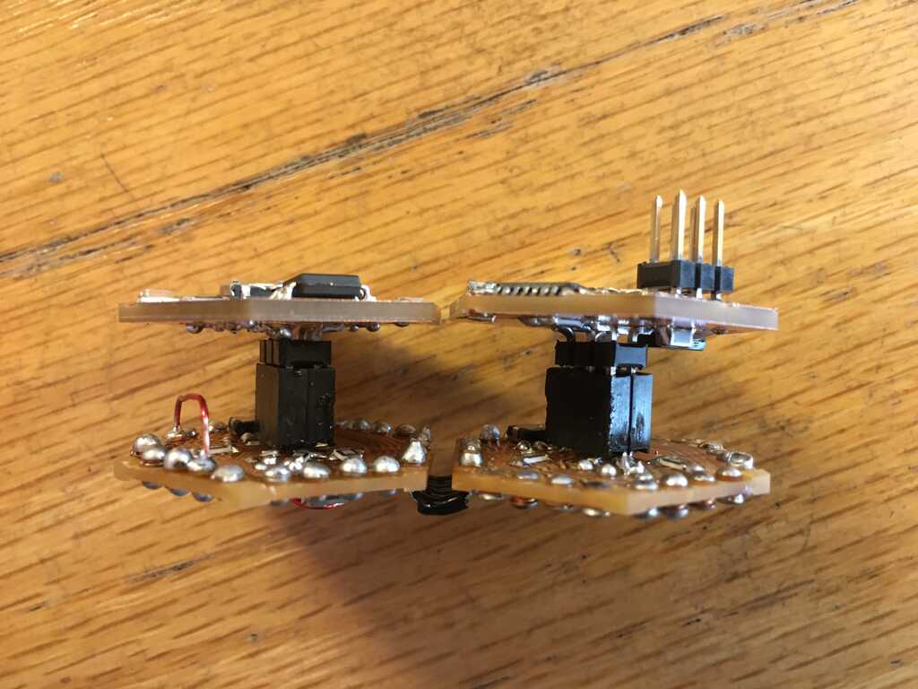
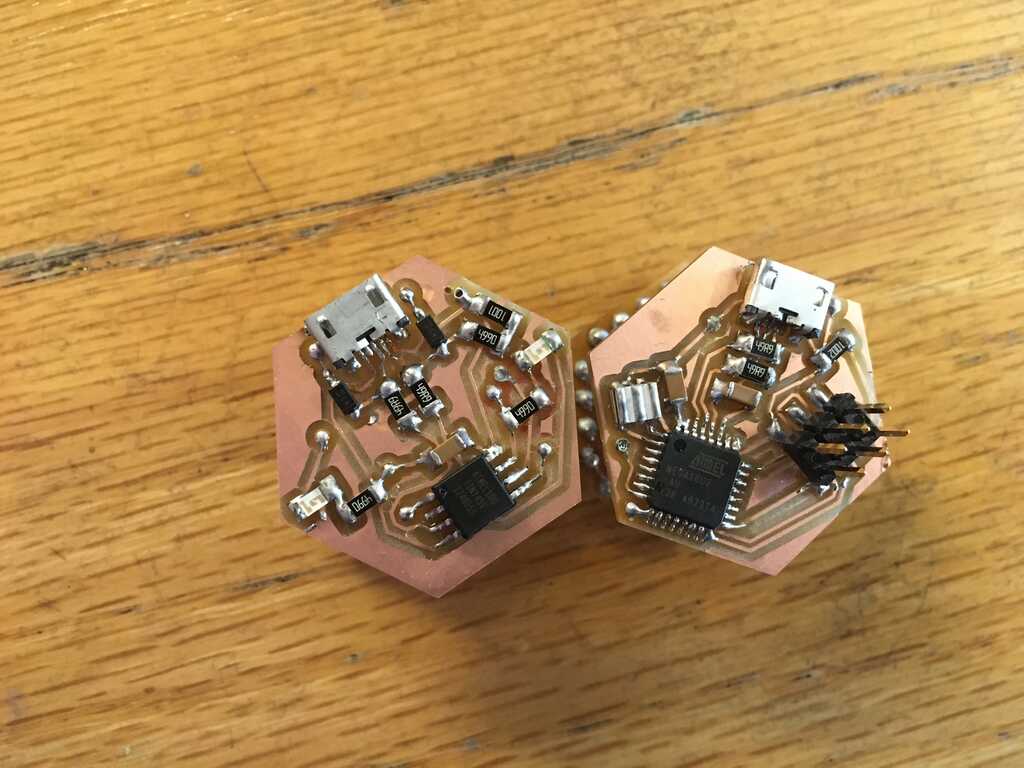
The first two boards I made my priority were the FTDI board (mostly for power) and the programming board (so I can program, of course). The programming board (right) came first, and I used it to program the FTDI board (left).
Check it, the FTDI board works! (The TX and RX lines are wired together)
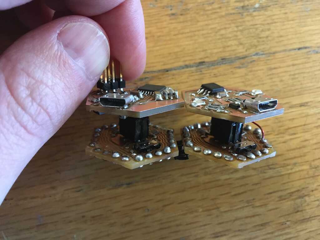
Now I could work on setting up all four modules.
Yeah, one of them had irreparable traces and another had the janky header tear off some traces, so I was down to two.
Nearing the end of my second day marathoning, I realized I didn't have the time to complete my overly ambitious idea for this week. So I slapped two of the modules together and got set on programming them.
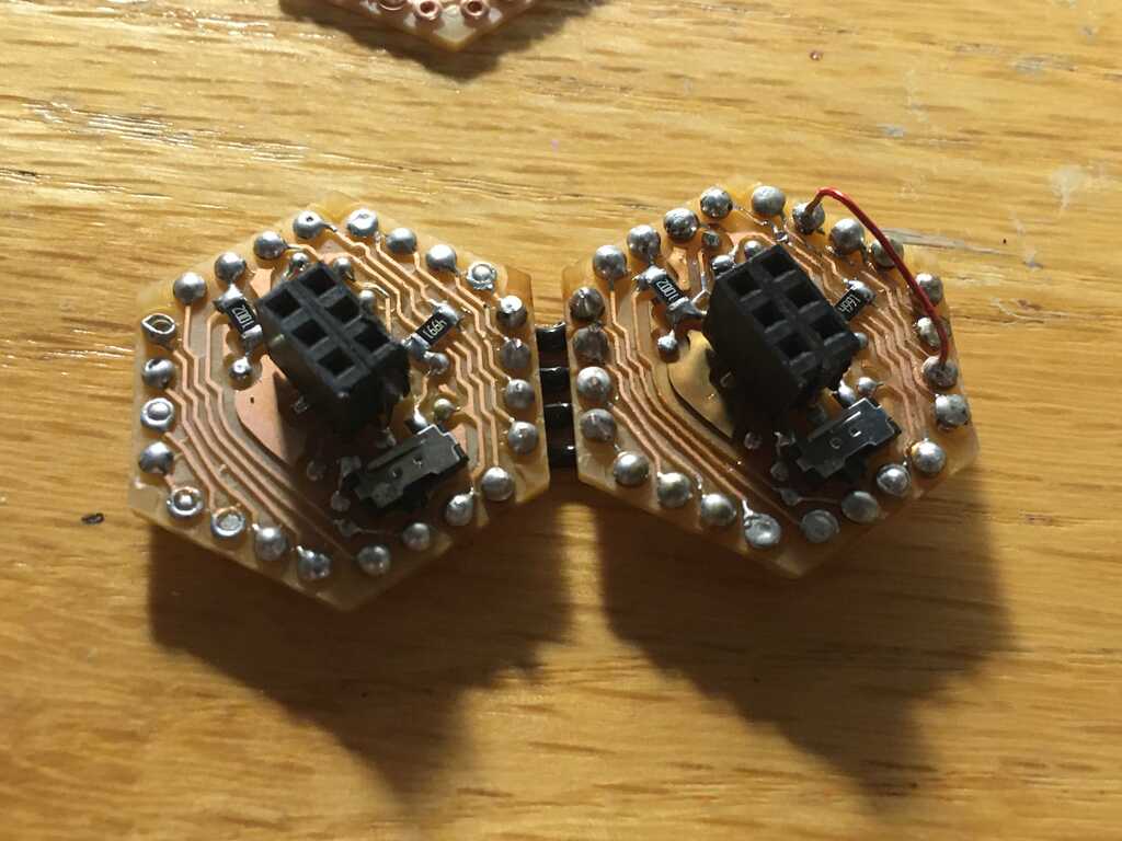
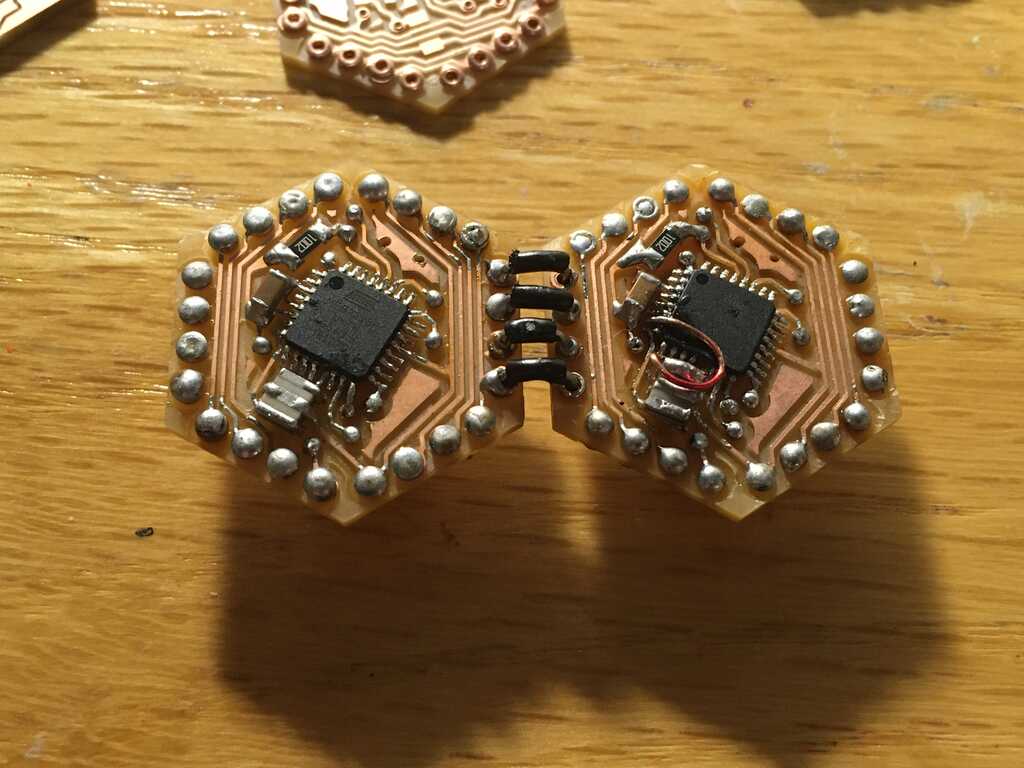
One of them needed a serious makeover, but that's alright. I can debug that. I needed to fill in the holes because there are connections that only exist through them, and nothing would work without doing so (in theory).
I need at least two modules at a time because one module needs to be connected to the FTDI board to supply power to the other one that's being programmed. Easy enough, let's hook them up:
Aaaaaand
No dice. No power going through (which is indicated by one of the programmer's LED). That means that something with the hardware (janky headers, broken traces, broken traces around holes, poor solder fill of the holes) is wrong. With office hours ending for the night, I thought to myself "no problem, I'll just come back in on Sunday and fix it."
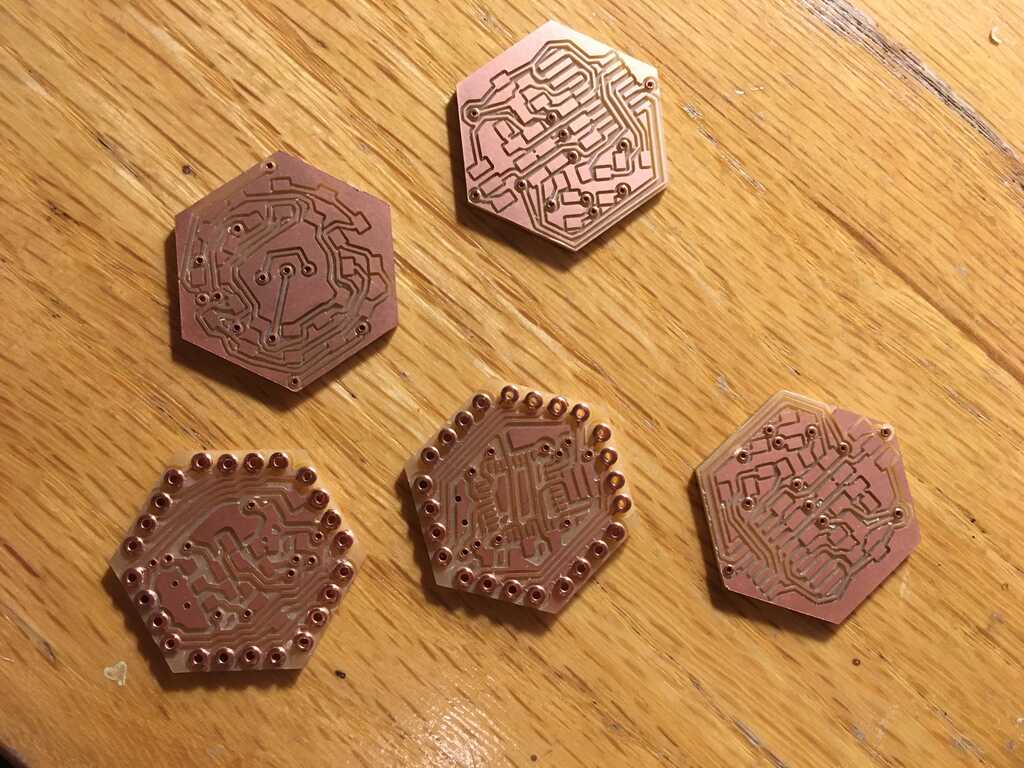
It's over
And then I got sick. I could barely leave my bed for 3 days. That means this is as far as I got. Look at this sad graveyard of boards that never got to fulfill their potential because of this:
But not really
Despite not being able to get the critical I²C experience I need for my final project, I still got some excellent design considerations taken care of:
- I finalized the microcontroller to use.
- I finalized the dimensions of the holes and board.
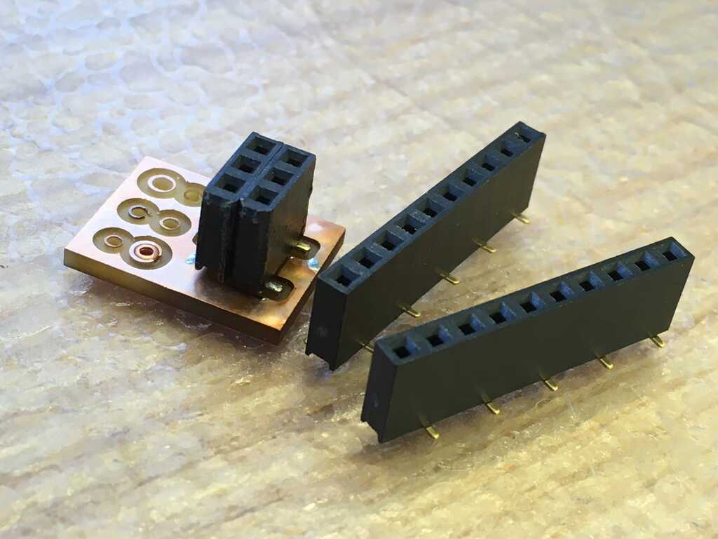
- I found some parts that will (hopefully) be a great size to connect the boards in an inexpensive yet "slim" form factor. (Female and Male headers!)
- How to implement USB Micro headers.
- The module board layout! That was quite a challenge.