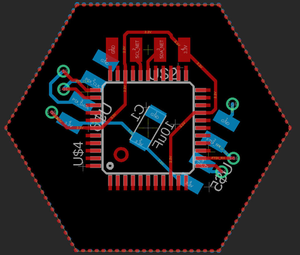
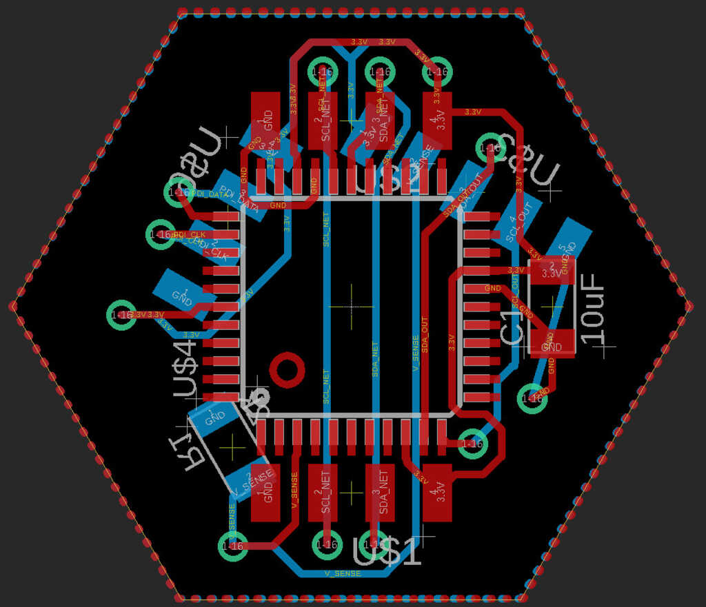
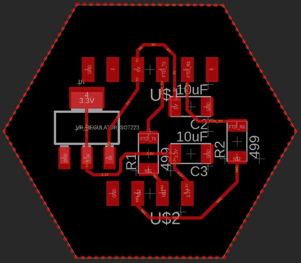
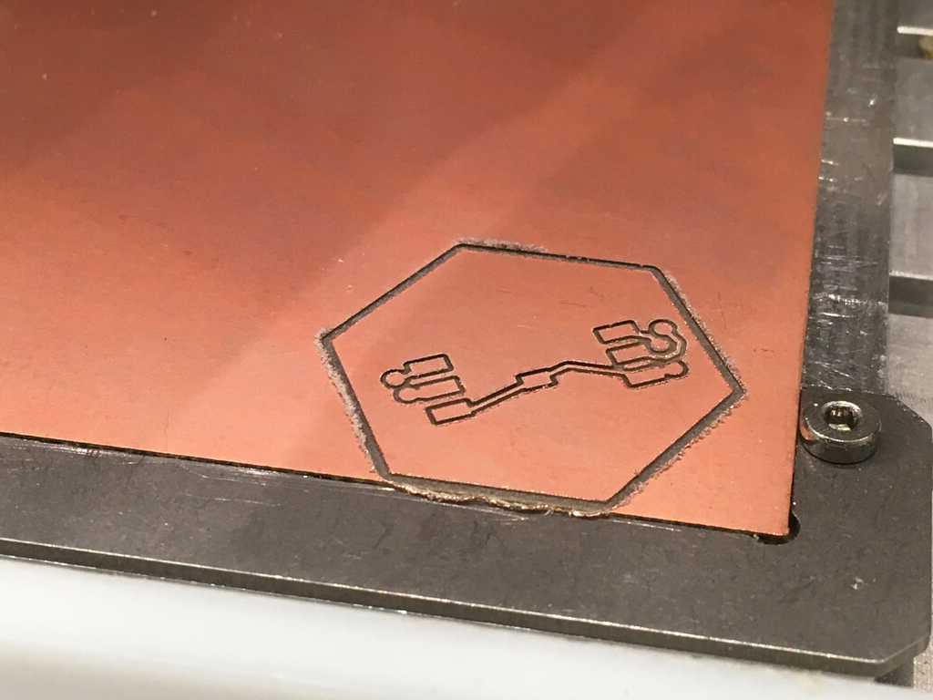
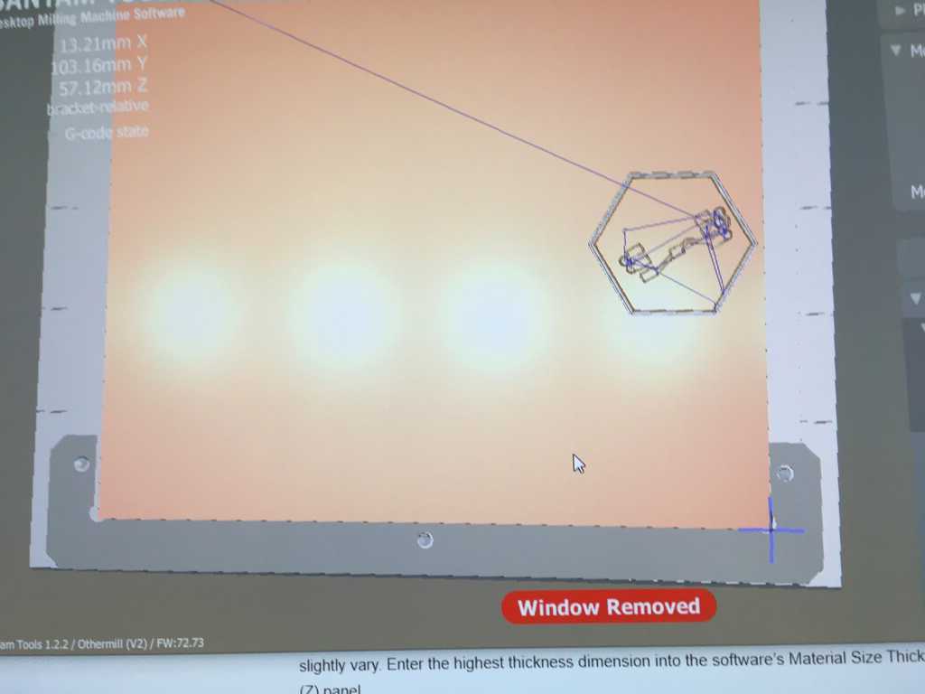
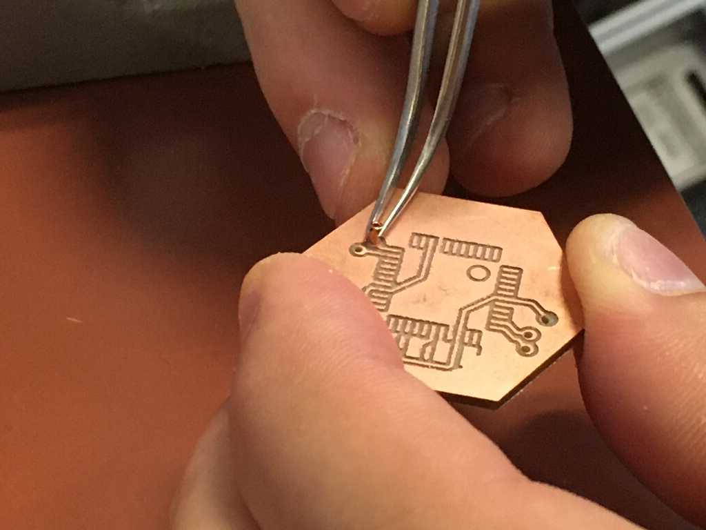
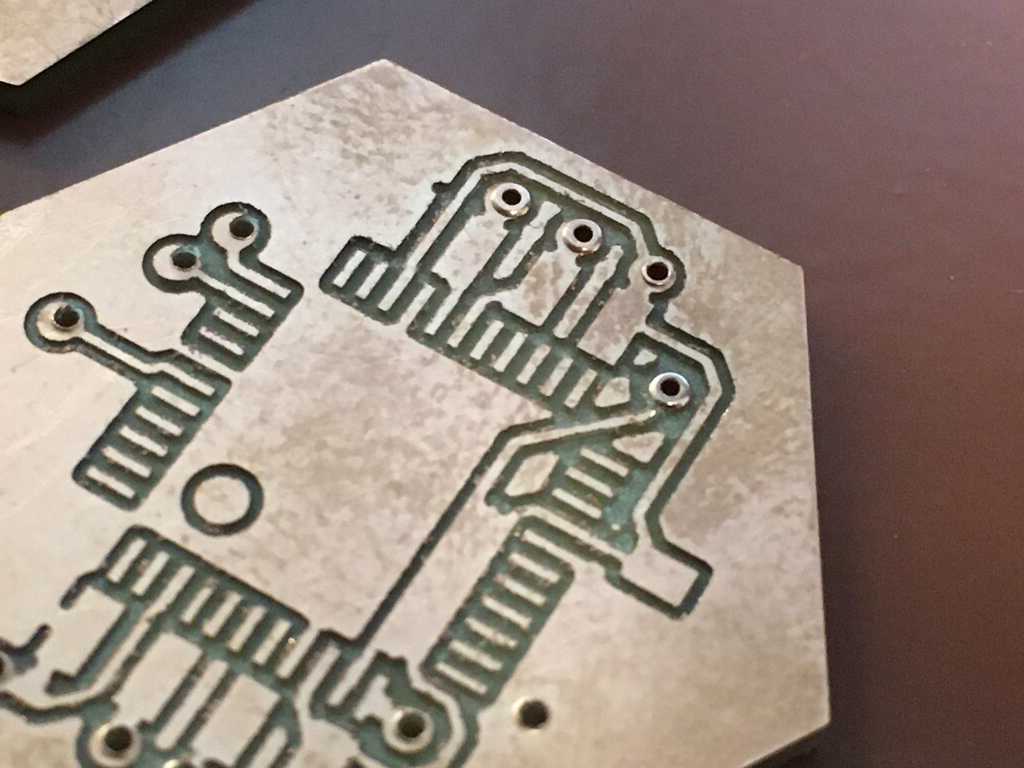
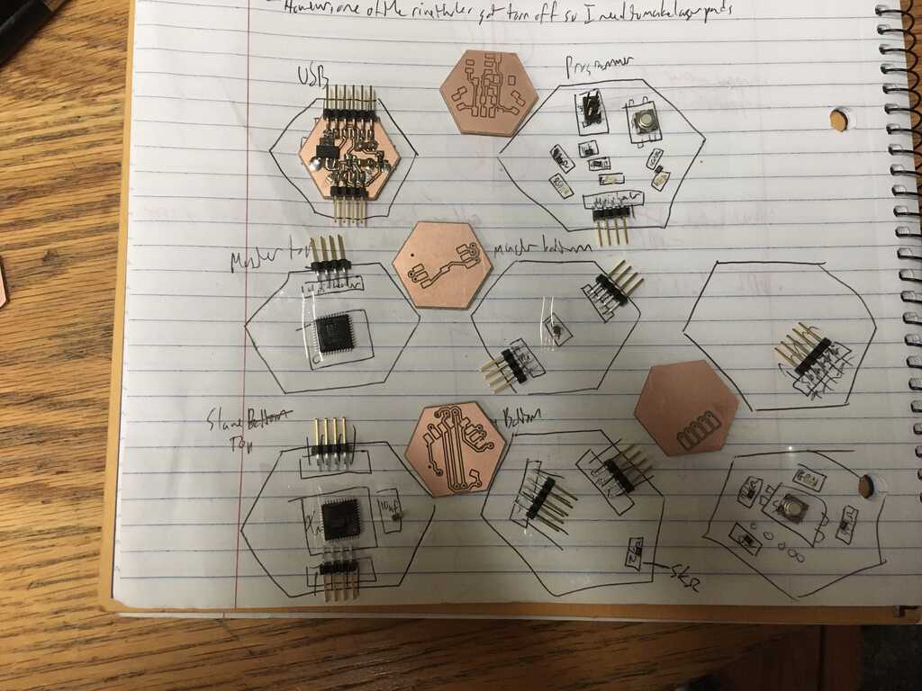
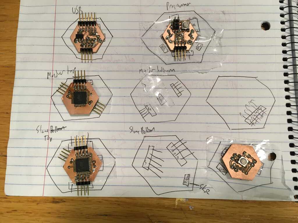
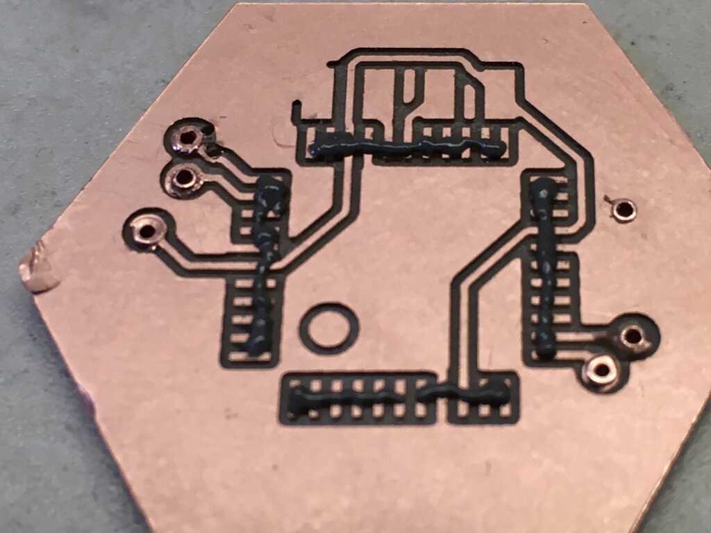
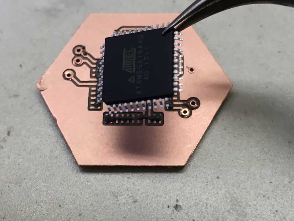
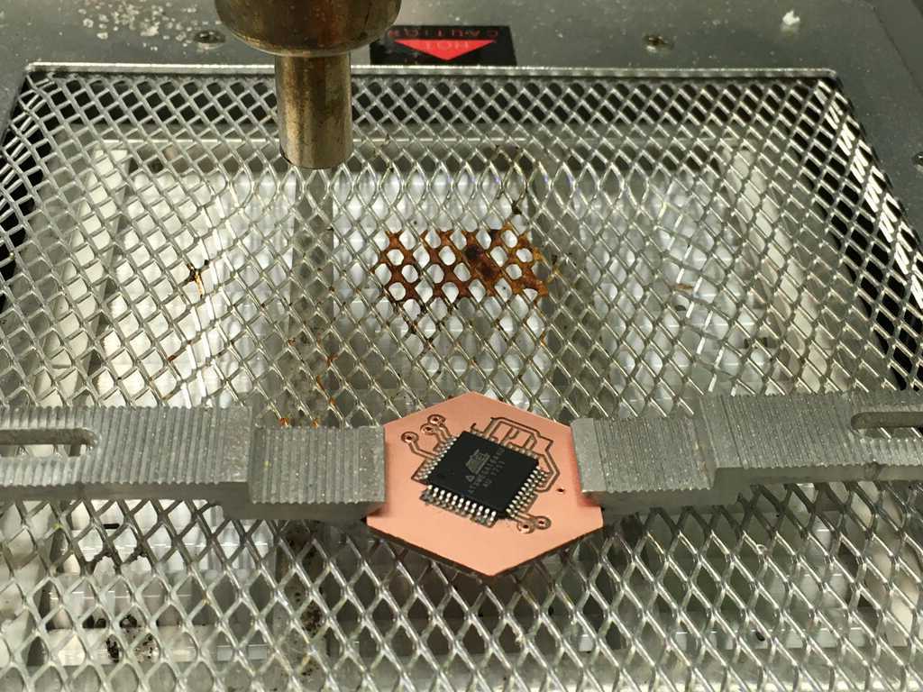
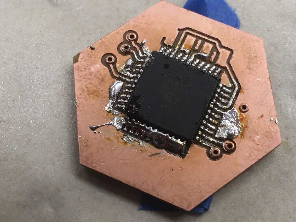
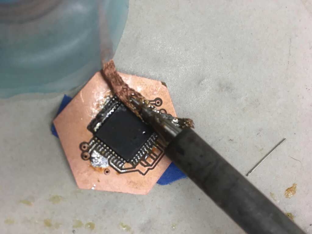
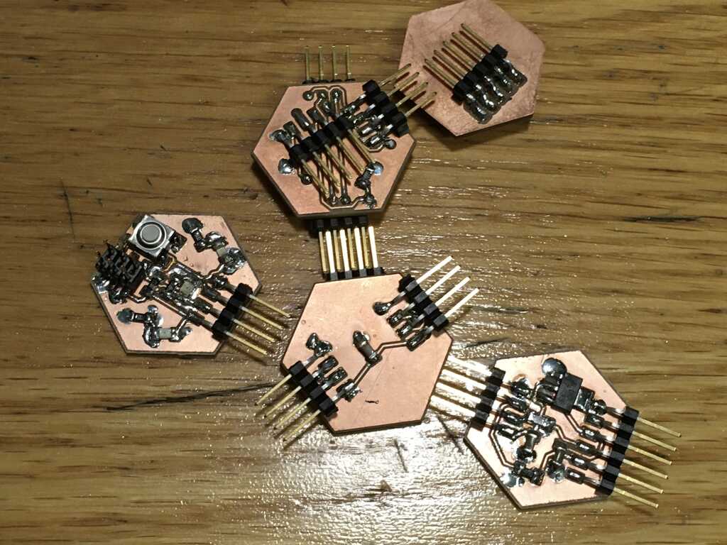
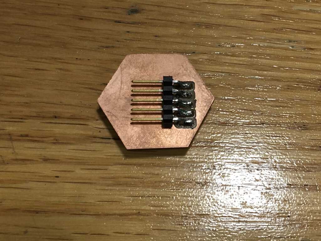
All boards use the same hexagon scripts from Week 3. Vias are .9mm in diameter for rivets. Traces are 12mil, which is as thin as I'm willing to go. I previously had bad experiences with 10mil traces. Most designs flood the entire board with ground, which is indicated by the dotted polygon around the circuits.
Download the Eagle project hereMaster:
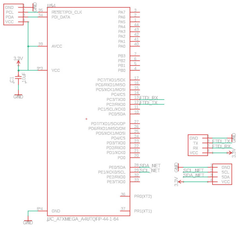
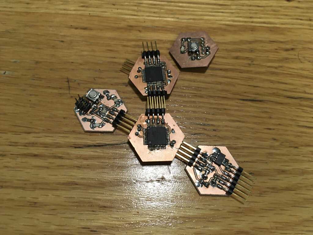
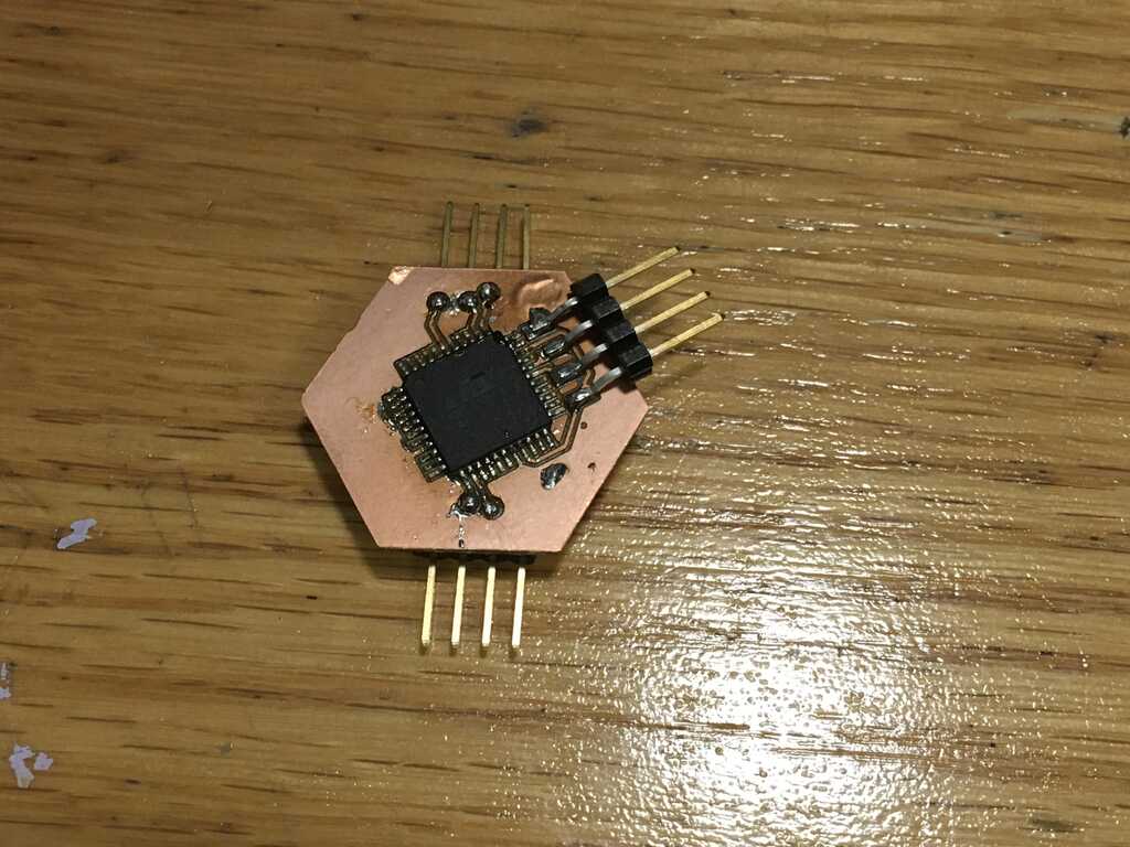
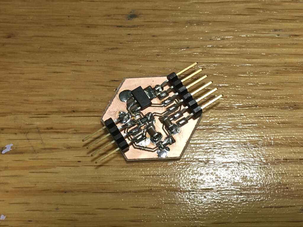
This board is fairly light:
- 1× 4-pin header to the programming adapter (PCL/PDA)
- 1× 4-pin header to the USB adapter (FTDI_TX,FTDI_RX)
- 1× 4-pin header to the I²C network (SCL_NET/SDA_NET)
- 1× 10µf bypass capacitor
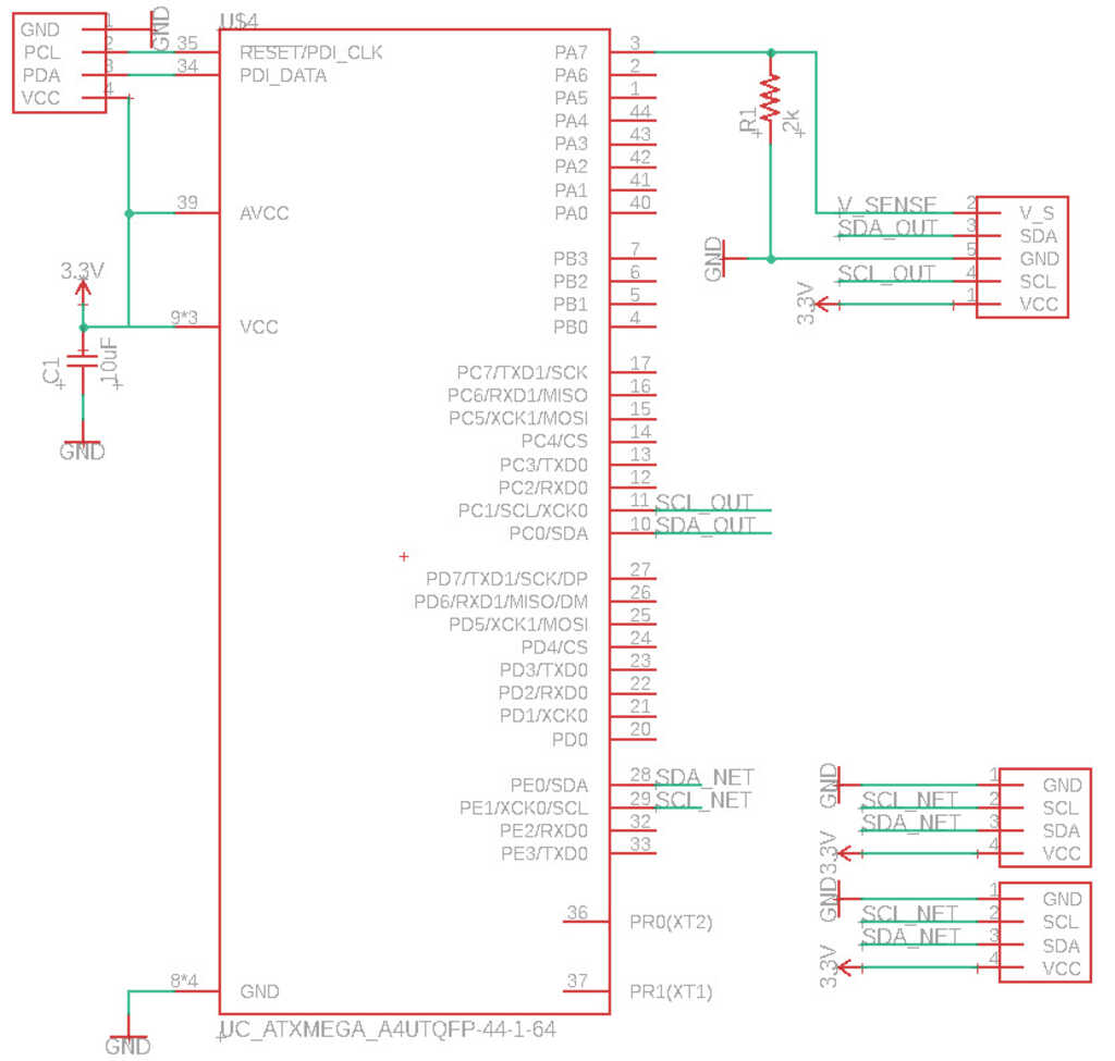
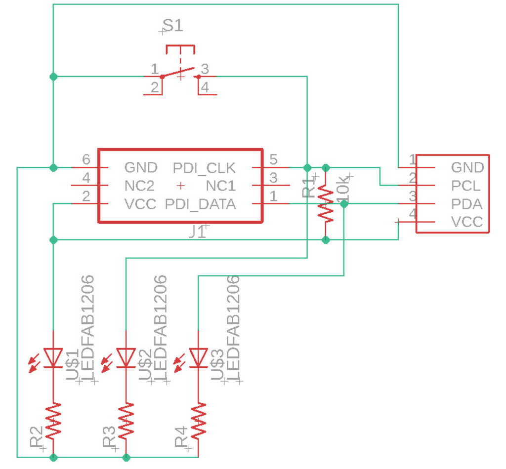
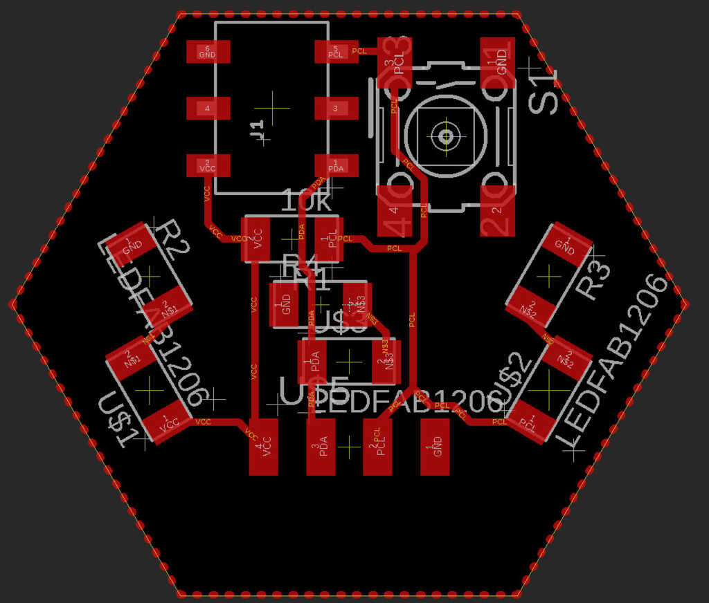
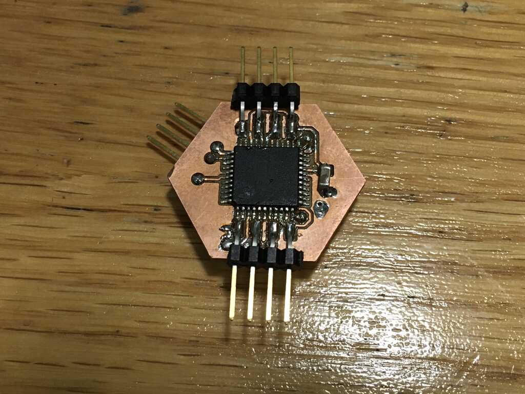
Slave:
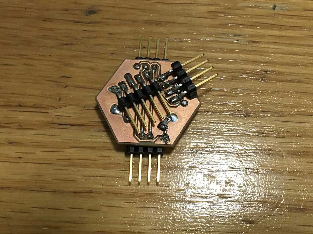
This board is much heftier:
- 1× 4-pin header to the programming adapter (PCL/PDA)
- 2× 4-pin header to the I²C network (SCL_NET/SDA_NET)
- 1× 5-pin header to the peripheral
- 1× 5kΩ resistor (in schematic it's 2kΩ, but I decided on a 5kΩ because there wasn't a 2kΩ in the shop)
- 1× 10µf bypass capacitor
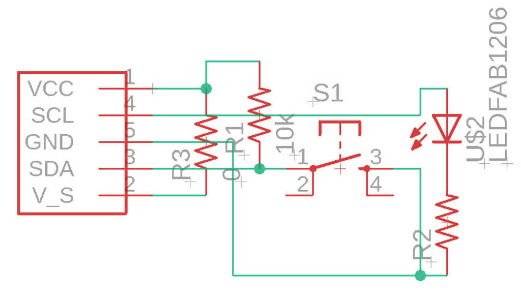
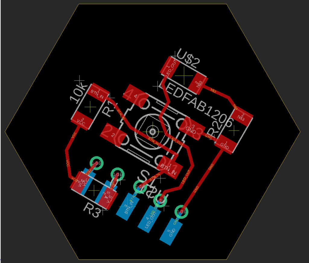
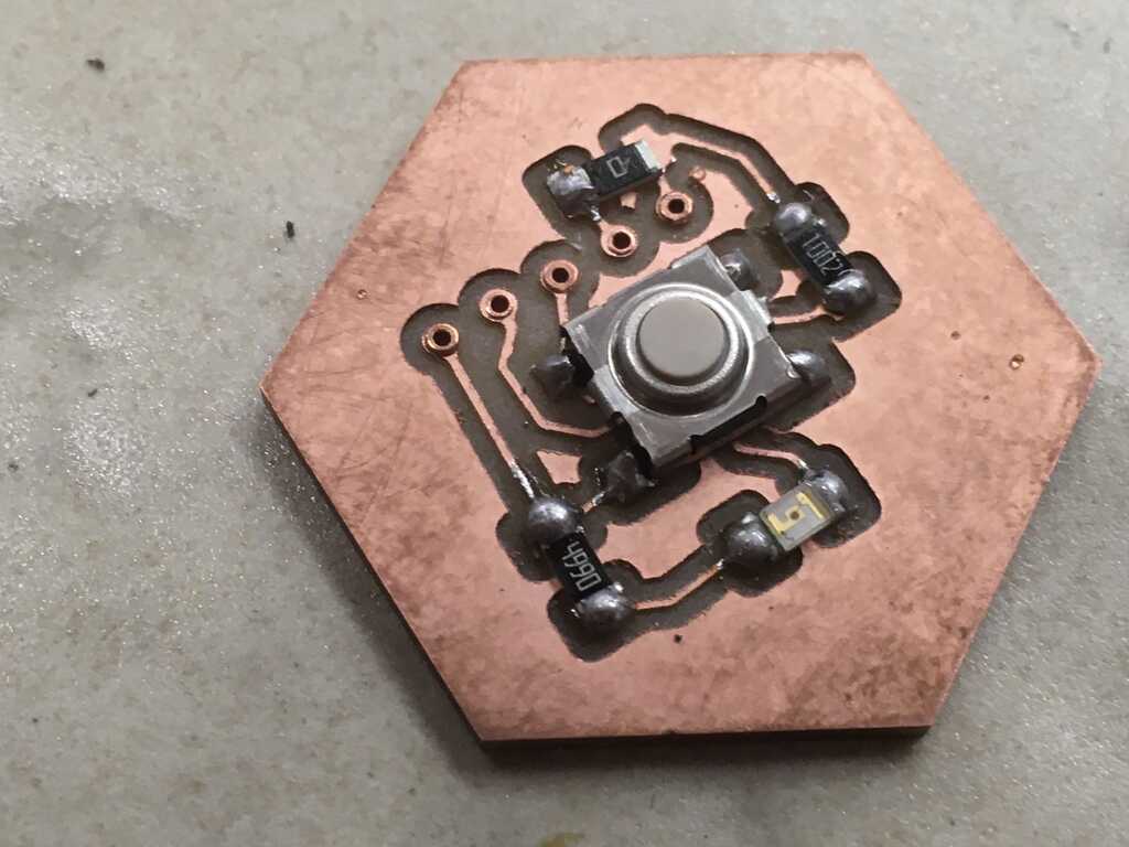
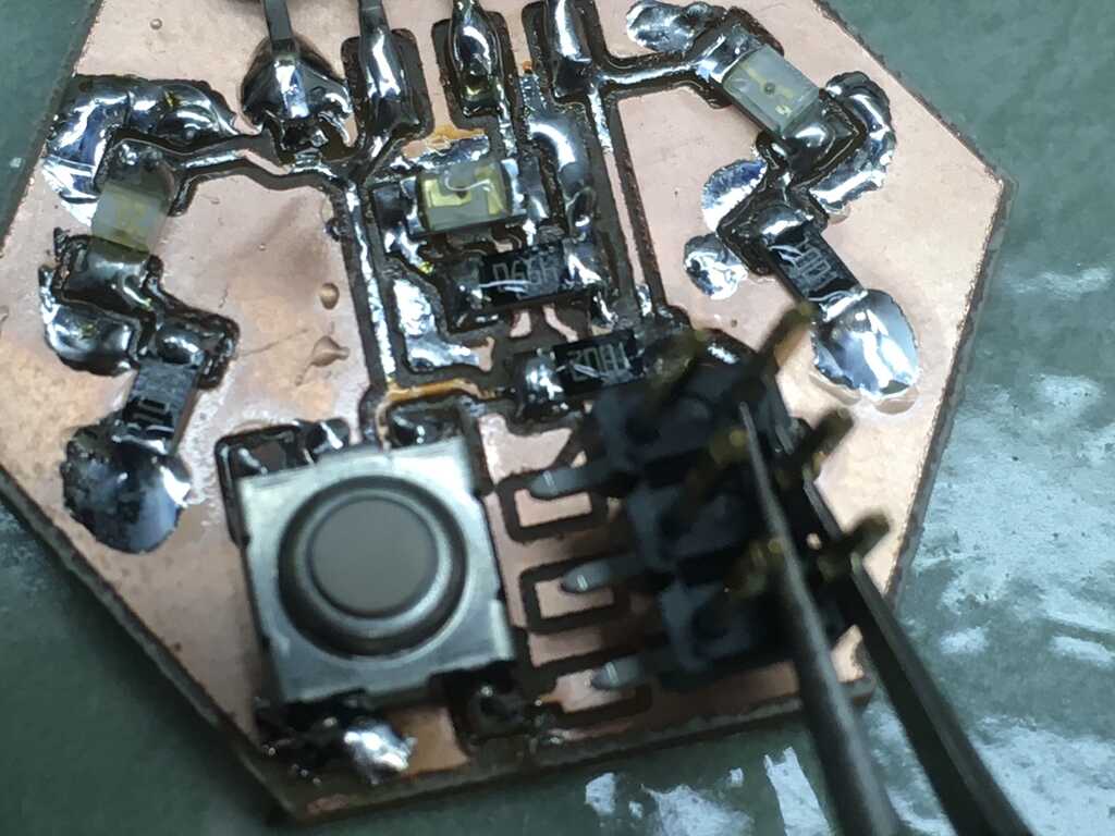
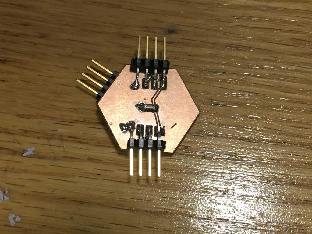
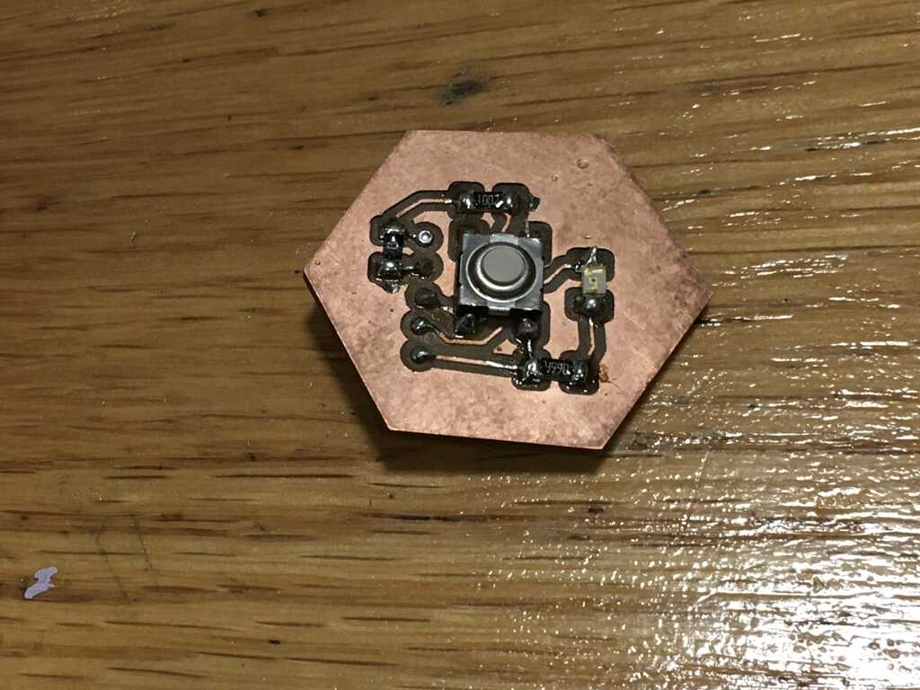
Peripheral:
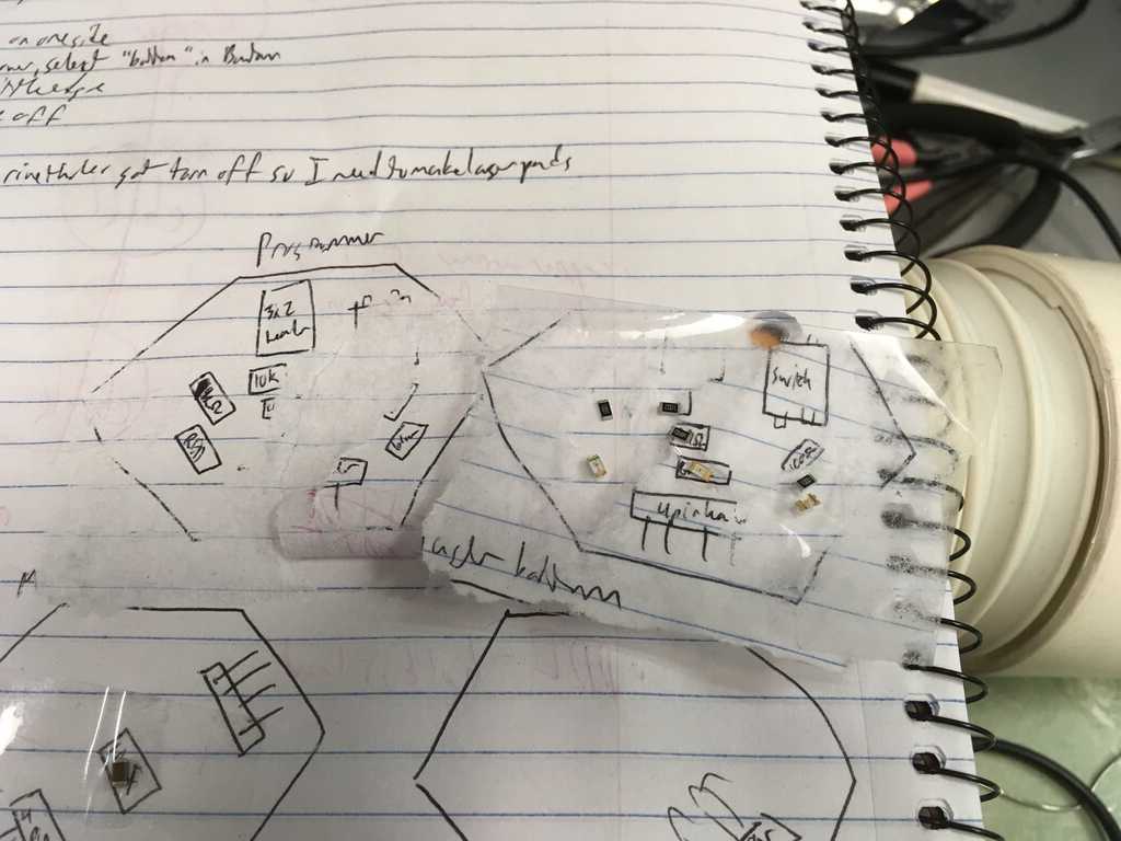
To meet the requirements for this week, this board uses an LED (attached to SCL), and a pushbutton (attached to SDA). You might be wondering "hmm, aren't SCL and SDA used for I²C?" and yes, you'd be absolutely right. The circuit was designed with the flexibility for the Slave to control simple components in the peripheral, as well as having more complex components that use I²C, such as IMUs. All it takes is some software to change what the pins do. Also note that this board does not have a large ground space.
- 1× 5-pin header to the slave
- 1× pushbutton switch
- 1× LED (in my application I used a Green LED)
- 1× xxxΩ resistor for LED (499Ω in my case)
- 1× 0Ω resistor (for V_Sense, this would make the voltage come back as 3.3V)
- 1× 10kΩ resistor (pullup for the button)
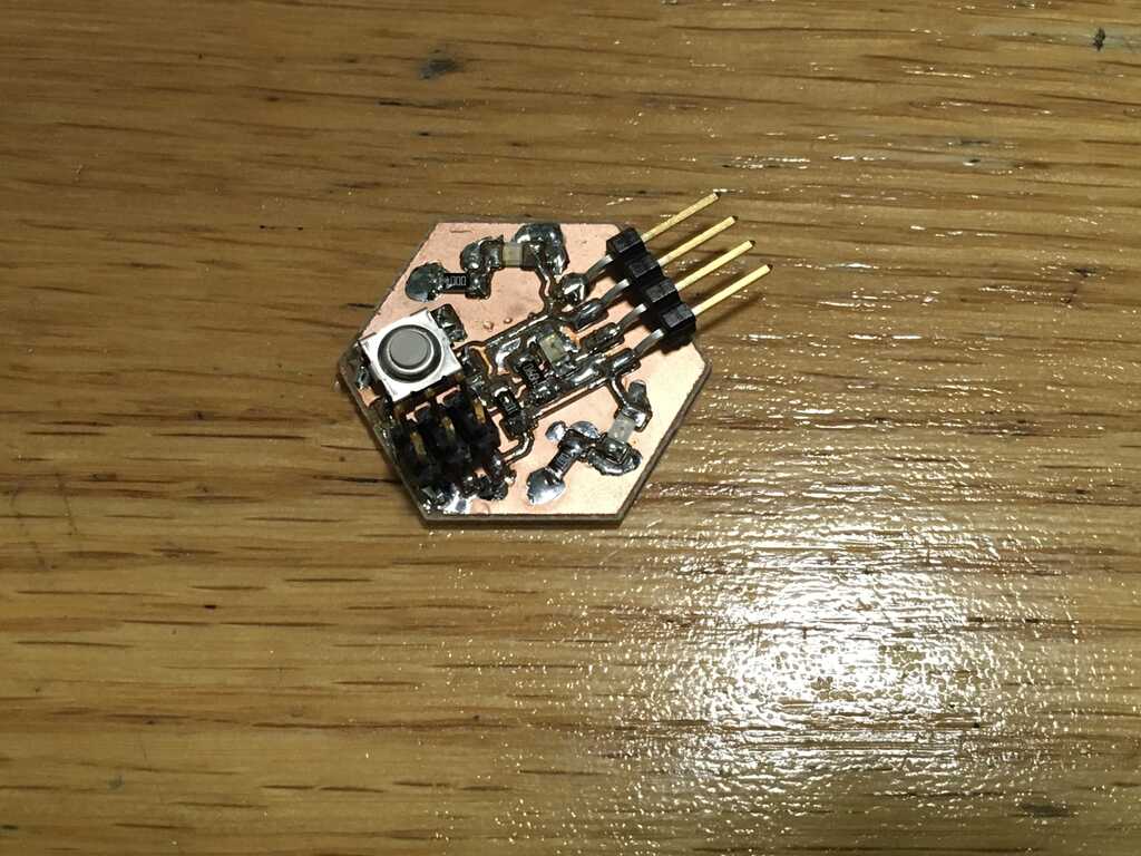
Programming Adapter:
This pares down the 6 pin connector to only 4 pins, which reduces the size of the programming header necessary on the microcontrollers. There are also debugging LEDs as well.
- 1× 3×2-pin header to a PDI programmer
- 1× 4-pin header to the master/slave
- 1× 10kΩ resistor (pullup for the button/reset/PCL line, since reset is active low)
- 1× pushbutton switch (to bring reset low for programming)
- 3× LED (any color, for debugging. I used Red [VCC], Green [PDA], and Blue [PDL])
- 3× resistor for LEDs (for the colors I chose: 1kΩ, 499Ω, 100Ω respectively)
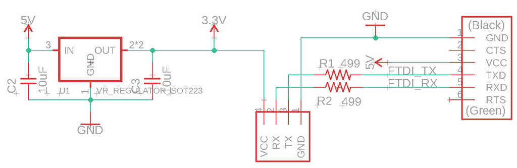
USB Adapter:
This also pared down the FTDI Connector to only 4 inputs, since we don't use 2 of them. It also brings the USB voltage from 5V to 3.3V.
- 1× 4-pin header to the master
- 1× 6-pin FTDI header
- 1× 3.3V Voltage Regulator
- 2× 10µf bypass capacitors
- 2× 499Ω resistors
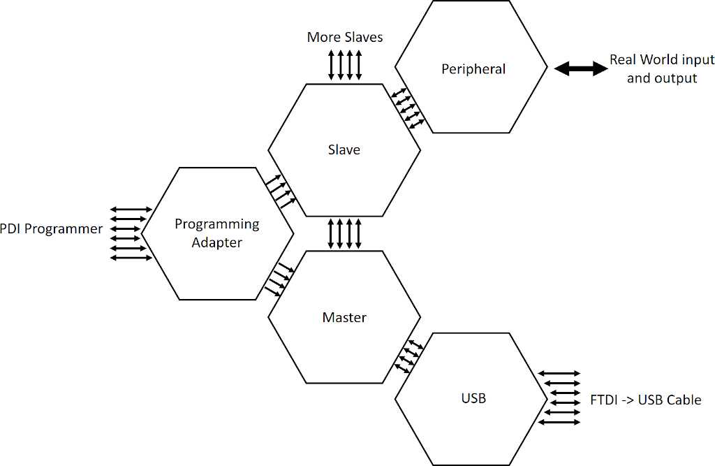
In general, this is how everything connects together. With I²C, it's possible for many slaves to wire to a single master. By week 7 I should be able to have at least 1 more slave hooked up.