
Source? *It came to me in a dream.
I don’t know if I first saw this on TV or in a dream, but I have had this idea to make glasses which can see CO2. In trying to find out if it was in fact a dream, I did a quick internet search to try and establish whether or not something like this had ever been conjured. I came across a group of people who did in fact not make a pair of glasses but rather a camera which has the ability to visualize CO2.
After further investigation and whilst simultaneously assessing my abilities and the scope of what this project would require I started to understand the 3 main ingredients necessary for a CO2 capable camera.
These types of cameras are called Optical Gas Imaging (OGI) devices, and they use a highly sensitive sensor made from a rare compound of InSb or Indium Antimonide. This material is well suited for detecting infrared radiation but are emitted by objects as heat. One thing which is necessary to understand is that these cameras are thermal cameras first and have the ability to also be detect gasses.
A filter is added so that it is able to capture infrared radiation between 4200 to 4400 nanometres (this is the spectral range at which CO2 becomes visible due to it absorbing the radiation.
Furthermore, the cameras are equipped with coolers (called sterling coolers) which cool the filters so that they can function and detect properly. This process takes around 5 min for the detection to even begin as the devices are cooled to -198 degrees Celsius or -324 degrees Fahrenheit. These devices visualise the gas emissions in a similar way to which thermal heat imaging is portrayed and the gaseous emissions of, chimneys, cars and airplanes are visible.
Reality
Getting to know and understanding the capabilities of this camera better I realized that if I tried to make or develop the design of a similar camera, not to mention if I try and make it a optical wearable, it would no doubt take longer than 1 semester at MIT and cost me more than the tens of dollars which we have allowed to us for the HTMAA course.
Taking into account the scope of the project, my limited understanding of electronics and the idea of spiral development I decided to simplify the design to something more achievable and aimed to understand/design a thermal camera and maybe turn it into a wearable if things go well.
Thermal Camera: Electronics Design
In my pursuit of designing a thermal camera. I have come across the schematics of someone who designed the camera for very cheap. Under $50 they say. Some might call me mad when I say that I am trying to understand this device through drawings, but as an architect this is how I do things.
This week we started off by trying to understand the tools we would be using to debug our electronics, which will almost inevitably become a thing which we would have to do. The reason for debugging is to try and find what is at fault with your work – weather it be a mechanical issue like incorrect soldering, PCB manufacturing errors or other things which I have yet to fail at. Issues which are electronic in nature can relate to code or closely relates to mechanics.
In the group assignment in week 5 we watched Quentin use the Multimeter (an item which can read voltage, ampere or resistance), the Oscilloscope (a device) which can read voltage difference over time, thus giving the debugger a deeper understanding of the fluctuations within the voltage of a system) and another implement which allows us to view digital fluctuations (the oscilloscope being analogue).
Reflection Week 3
I learnt that voltage can be negative or positive depending on the directionality of the black and red measurement stick. Also, that a change in voltage can also relate to the commands or codes which we tell an item to do, and in understanding this, we can see if an item is functioning correctly.
For example, if I code a servo motor to move at 4000ms intervals, this will show up on the digital or oscilloscope as spikes every 4000ms. The oscilloscope also measures human input and can fluctuate depending on a human’s interaction with a device (for example a spike when a human presses a button and let’s go of the button.
Electronic design Workflow
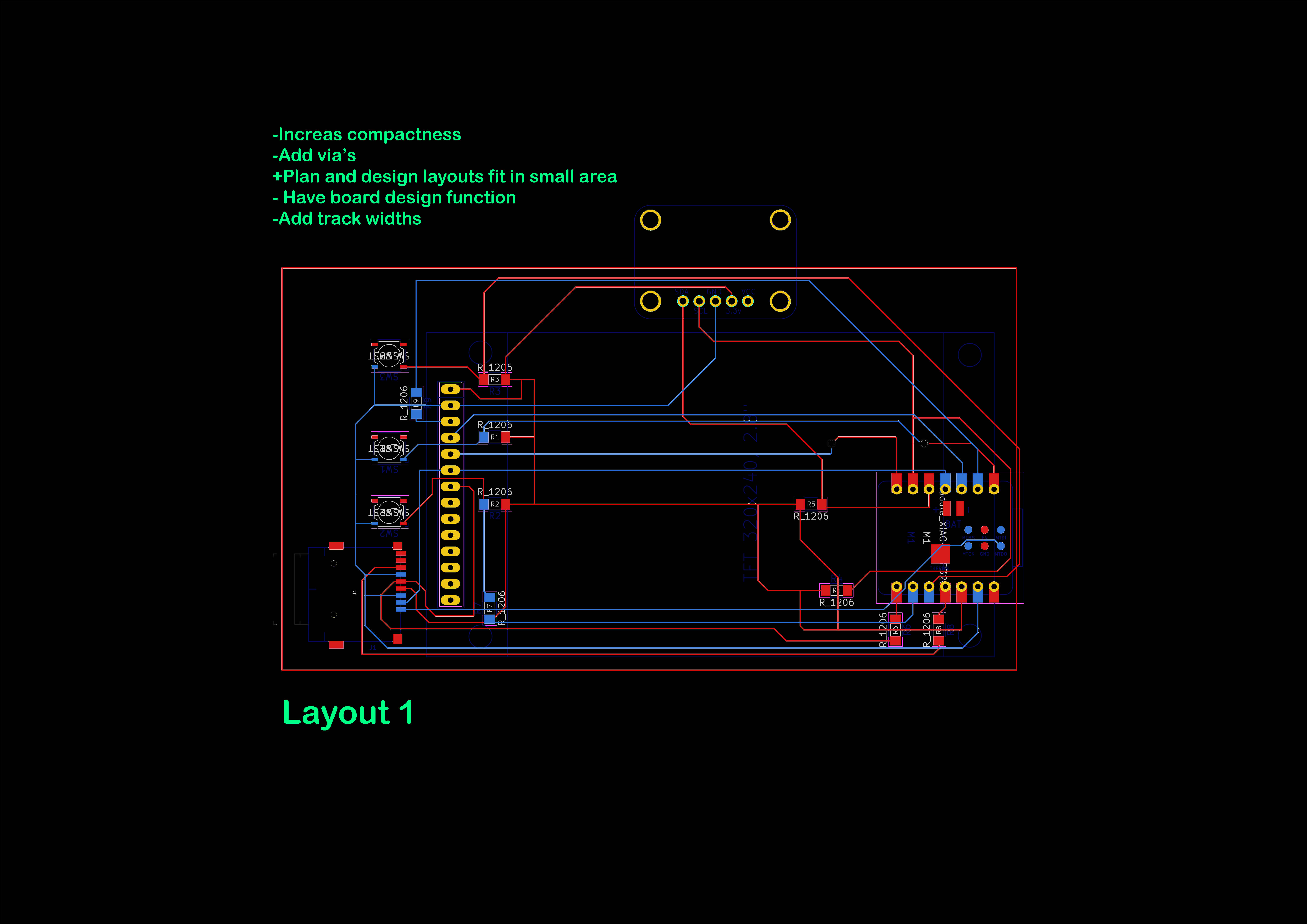
If I was going to try and understand how the PCB board was made, I had to take a step back. I had already drawn the components on paper and connected them on photoshop, but this told me nothing about the actual sizing of the components.
The next step was going to be to see how compact I can make the wiring in KiCAD. Although this week’s exercise might not result in a PCB for the eventual design, it might lead me further down the path and closer to the goal. I am essentially working towards the middle with the final product as an example and my own understanding as a starting point.
To see how small I can make the PCB board I decided to move around the components to see how they relate, and which configuration might be the most optimal.
Much like in architecture, by redrawing things you start to understand individual components and the greater scheme much better. I understand that I do not yet have all the answers to accurately understand how this system functions, at this stage I need to be able to ask accurate and the correct questions.
Firstly, I was trying to understand my role in the design, to try and separate component from design and PCB. By studying the existing PCB boards, I learnt that GND points are not necessarily connected to one another, however they need the same voltage to act as a baseline for the rest of the system. I also learnt how KiCAD functions, however I have yet to master it. I associated the Schematic symbols to their footprints manually because the components were not necessarily available at MIT or otherwise locally.
My initial attempts at recollecting my very limited memory of electronic design. I did this to form a lexicon for the purpose of reading the existing electronic schematics. This was going to be my Rosetta stone.
What I discovered when I redrew the images the first time is that each wire number corresponds to the correct port in of a different component. This gave me a vague understanding of the relationship between some of the components.
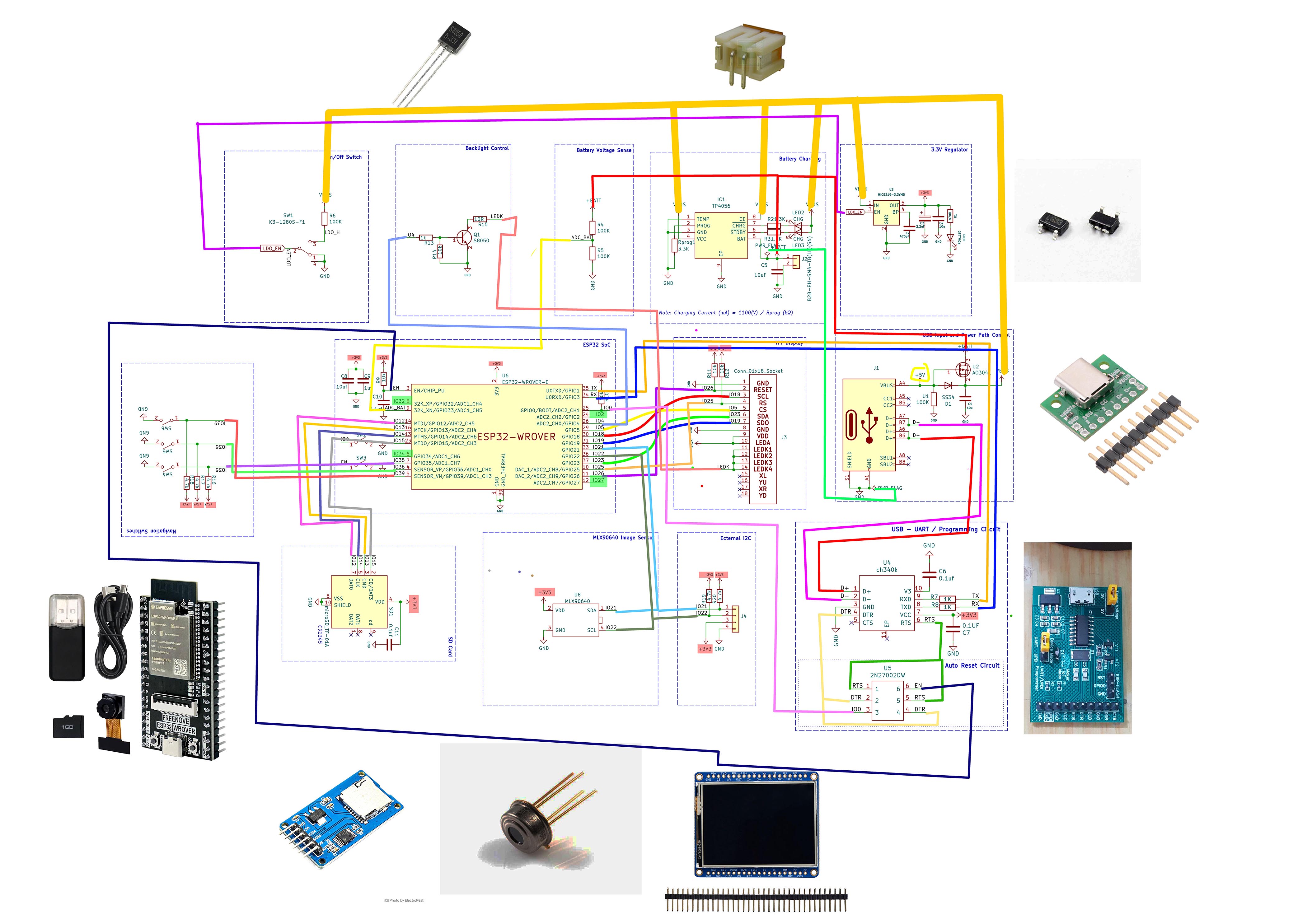
With this image I was trying to understand the functionality of the system. I started off by arranging the components according to how the user might use the device, and to keep the wiring as simple and efficient as possible. In essence I was simultaneously trying to become more confident in my understanding of the relationship and importance of each piece of electronics.
This previous step helped me when I repeated the connections in KiCAD (so to eventually try and optimize the design). Understanding the interface of the program was relative to manage as this is my first time using this program. I am also trying to understand the scale of the electronics so as to know if adjacent wiring will interfere with each other or have enough space to properly function.
At this stage I gave up (for now) trying to produce a fully reproducible PCB board for the thermal camera. Instead, I tried focusing on what the lines mean (yes, I am at that stage). How the components relate to the wiring, and to what extent I can use KiCAD to try and simplify my workflow.
The actual sizes of the components placed up to the wiring diagram, this shows the space for optimization in sizing of the components and gives you a better idea of what the eventual scheme will be like when the PCB is produced.
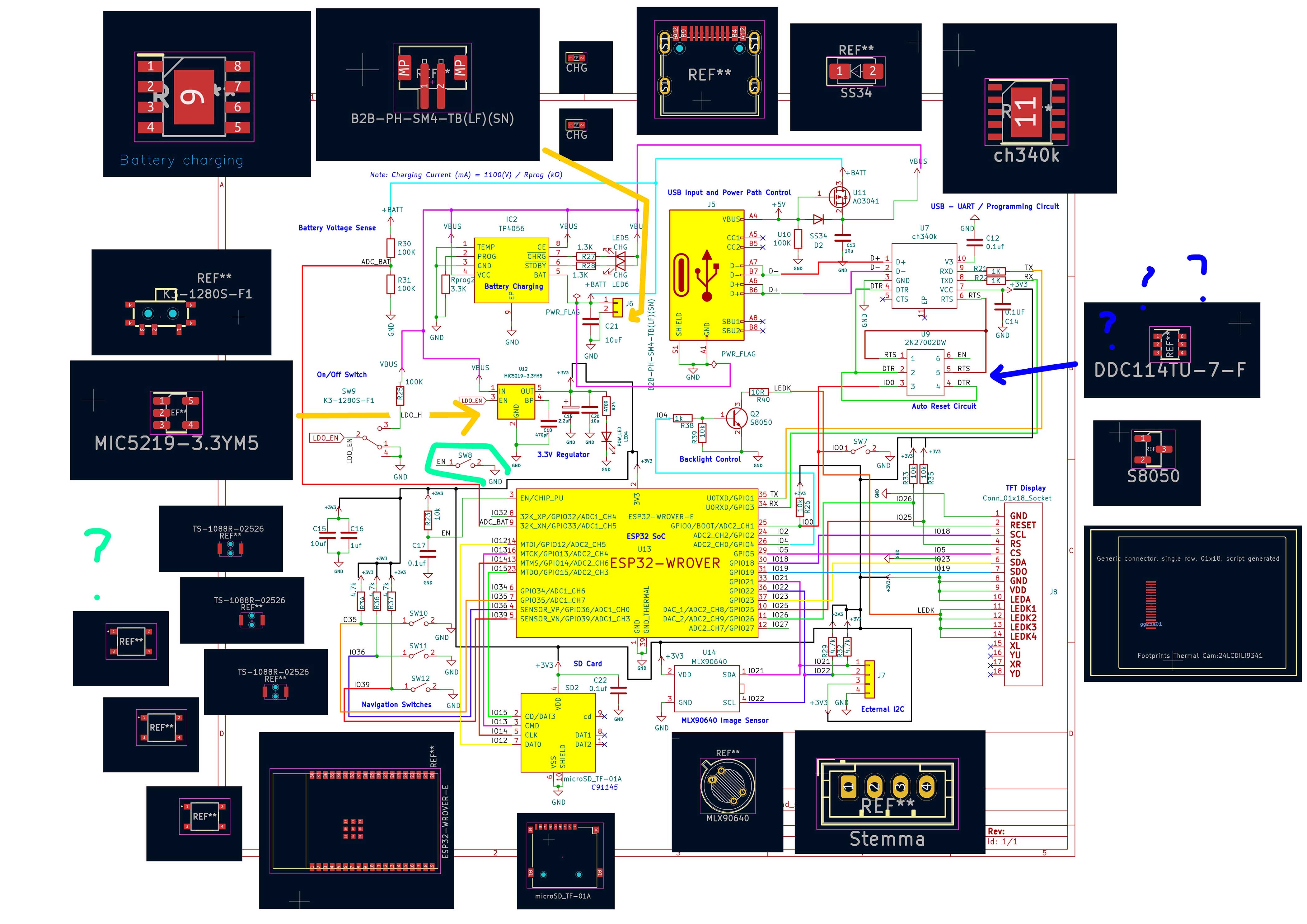
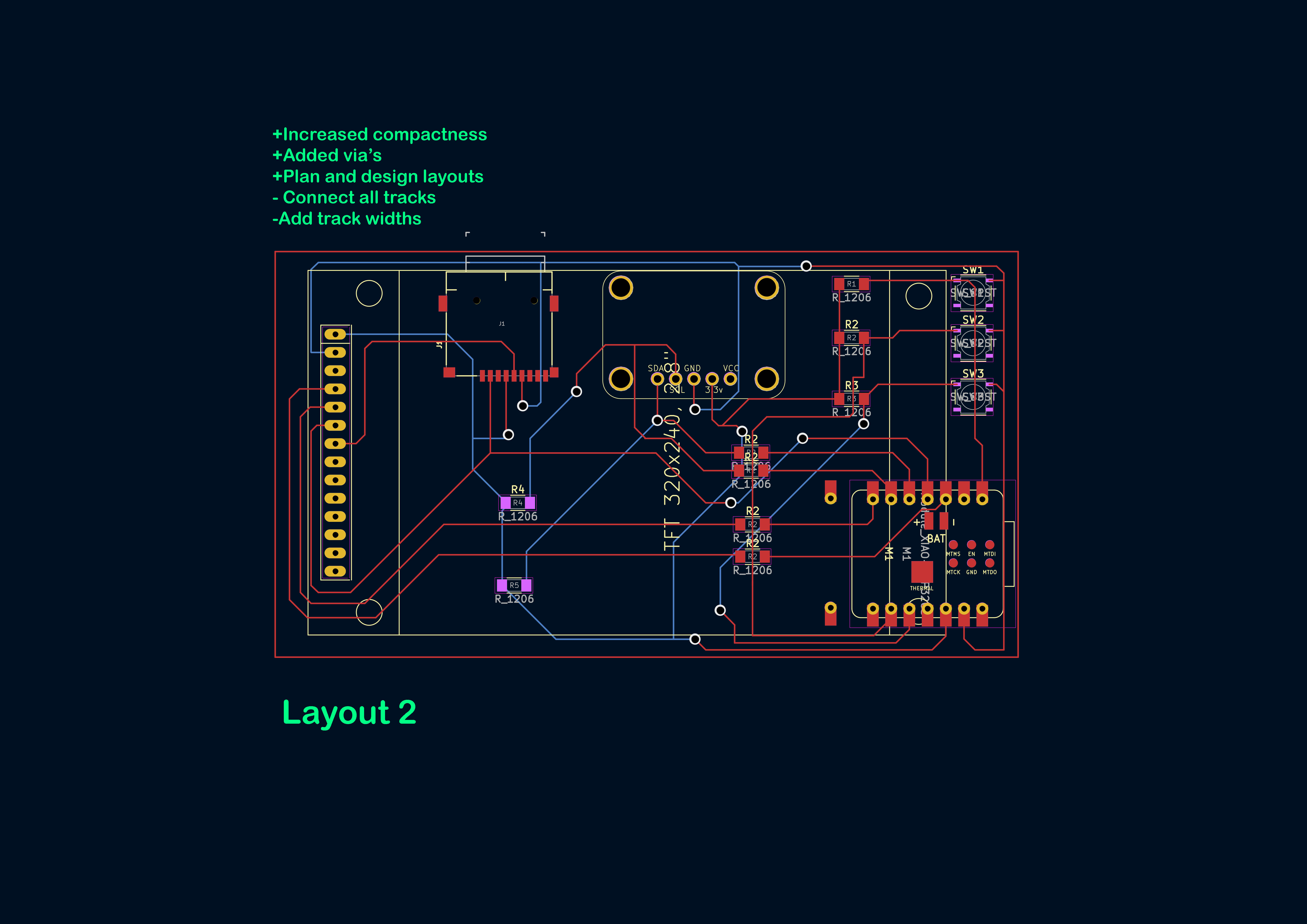
I had consulted Anthony and some of the other TAs about my project throughout the semester. Anthony told me that I could essentially simplify the existing design by at least 50%. I removed the backlight control, the on and off switch, the battery voltage sensor, the battery charging, the 3.3v regulator, the USB-UART/ programming circuit, auto reset circuit, ecternal I2C and some other smaller redundant switches and components.
This significantly improved the chances of me getting a working prototype at the end of the class. I could tell that my limited knowledge of electronic design was increasing because my questions to Anthony were less likely to be “what do these lines mean?”, as the semester progressed.
I also set out my limitations and the scope of what I hoped the end project would be in the bigger scheme of things.
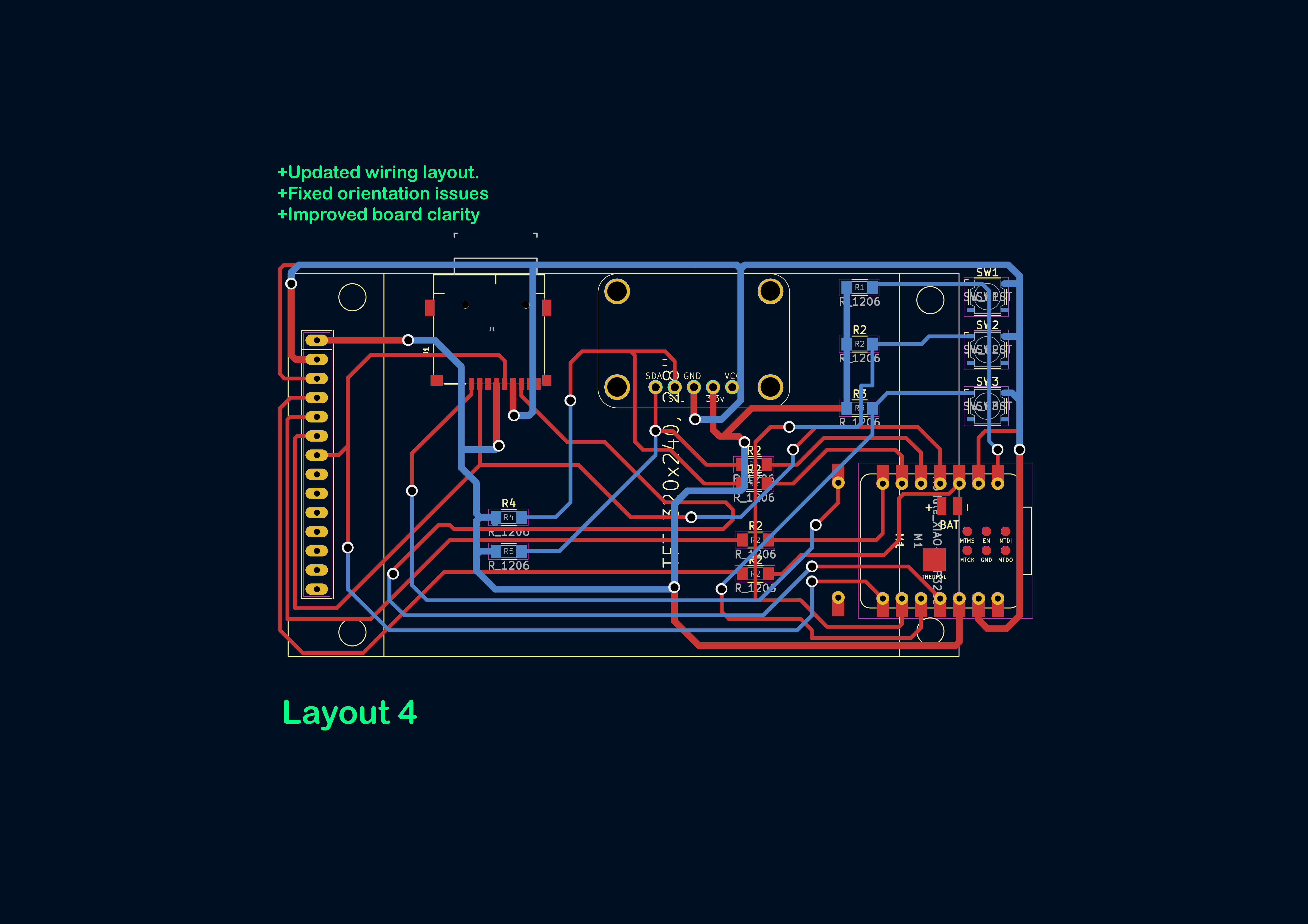
Schematic and PCB design
The final PCB and Schematic has several considerations.
Firstly the correct size and components needed to be understood so that the initial design could evolve in the correct direction from the example.
I was also considering whether I am going for a handheld or a wearable device. My initial ideation was relating more towards a pair of glasses, but I ended up deciding on just a normal hand held, and tried to keep the form quite small.
I sketched up a rough design layout for what the device would need to achieve. The existing thermal camera schematic was of help for this and I took some of the layout as precedent. With the help of Anthony and Diana, they helped me to understand the components and how they fit into the bigger picture.
A deeper dive into the electronics helped me come to an understanding of the features and (possible) failures of building such a device. The mismatch in languages which the components speak to the microcontroller with could possibly result in problems along the way with regards to the speed at which the device works. However, there would be a tradeoff because I could have the final device share wiring across the SD card and Screen Wiring (Both of them were communicating using SPI).
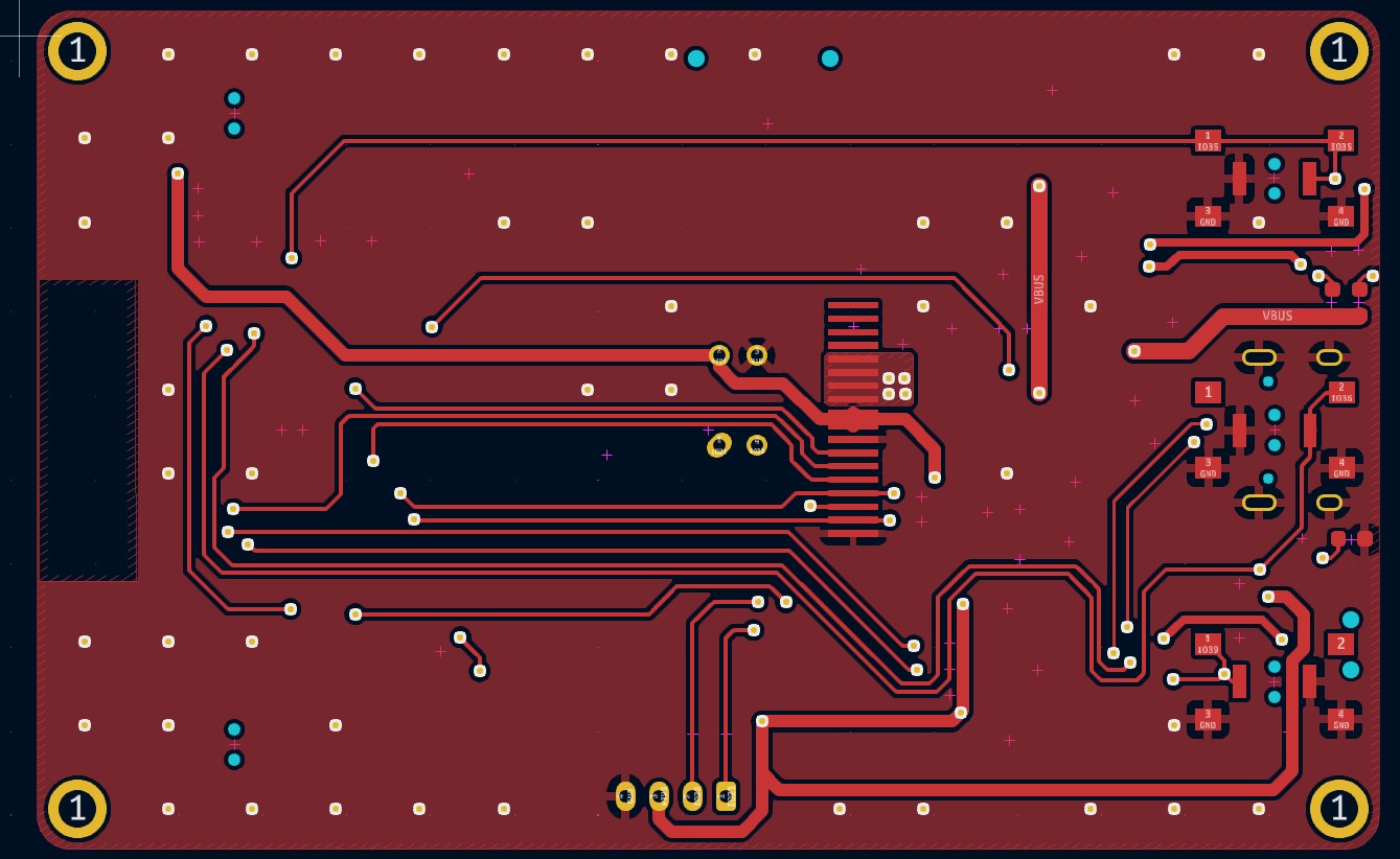
Then the PCB scheme had to be as simple as possible to be able to accommodate the most components, in the most effective way. I also tried to keep jumps from the one side of the PCB to the other to a minimum.
I would probably say that the adage ‘Measure twice, cut once’ was most applicable to me. Especially when you are setting up your project. Especially because of limited resources. For me personally it also helps to understand the component and maybe try to have a physical one in my position before I try and start up. Perhaps I am paranoid but I would like to eliminate the most amount of errors before I start.
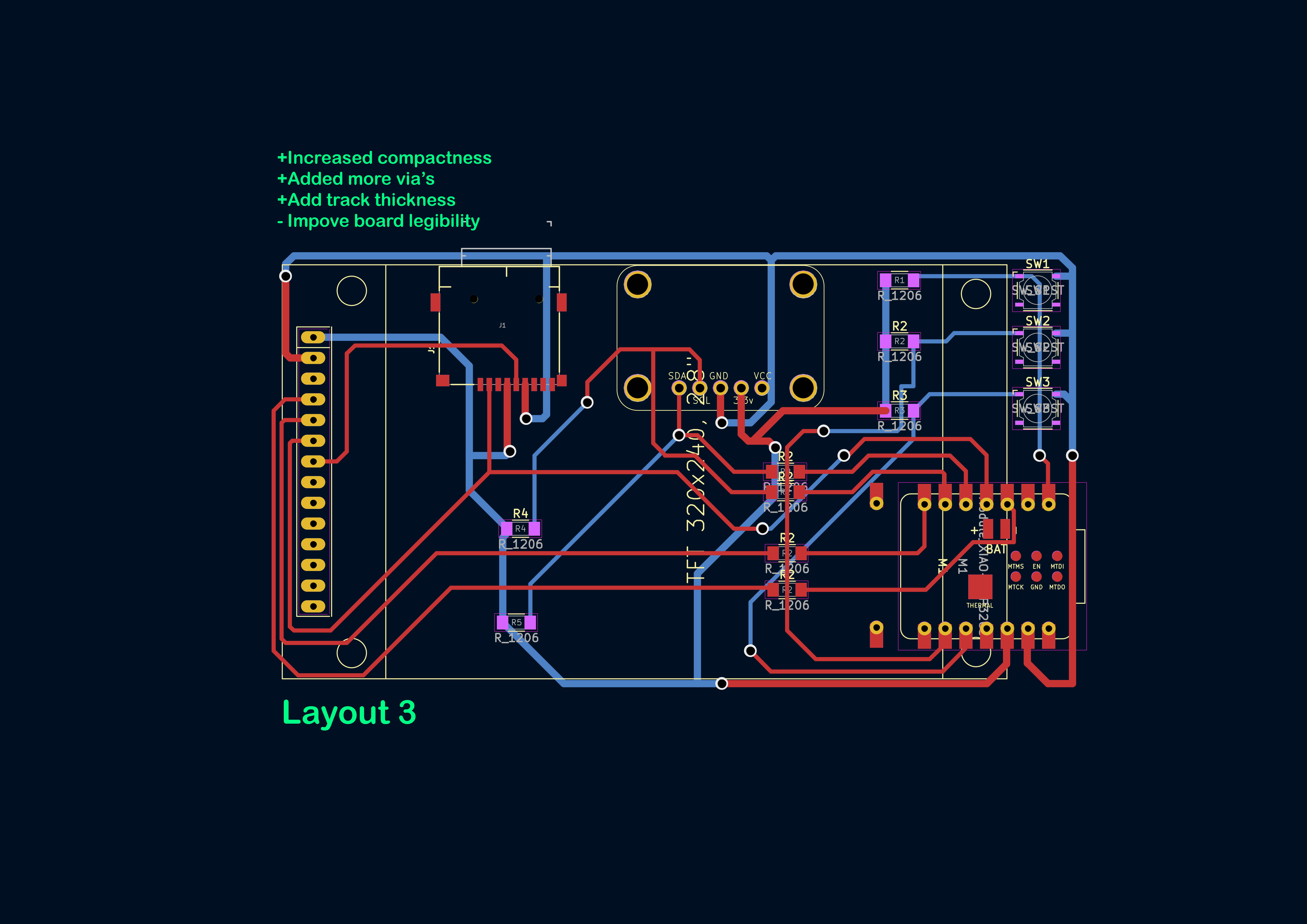
I think keeping track of which way the reverse board is going is also quite difficult. I would equate it with trying to figure out the inverses of inverses during the molding and casting week.
Another thing which I noted during the PCB design, was that adding resistors to jump over cables disrupts the netlists in KiCad. I had to resave everything and move the PCB, Schematic and General file into a new folder to have the PCB and Schematic be ale to communicate and update accordingly.
Mistake 1
After I finally fixed the writing and matched everything up. I realized that because the back of the PCB would be flipped. I made a mistake in inversing the XIAO.
Me and Anthony were speaking past each other, but once we got on the same page about what is ‘Up’ and what is ‘down’ I started to understand things better. I decided that the minimal effort would be the latter and to mirror the Thermal camera and the TFT screen.
I also ordered the parts and made sure to take into consideration shipment time. I had to choose between the 110-degree camera and the 55-degree lens. I chose the 55 degree lens because I was more interested in focused and accurate imaging as opposed to landscape shots in thermal.
Assembly – Milling
I started milling my PCB on the machine in the EECS EDS labs. After I started the machine began to malfunction and Dave had to rescue it. This was because the motor overheated and that caused some of the 3d printed plastic parts to melt.
EECS EDS labs have a nice printer because it takes standard copper plates and those are pressed up against a stop bar on the front side of the spoil plate. This means that there needs to be less adjustment when milling on both sides of the copper plate.
The EDS machine also works with direct Gerber files and does not require PNG transmission like the ones in the Arch Labs.
Assembly - Vias
I finished the board, and it came out nicely (with some assistance and reassurance checks by Dave and Anthony). Initially I thought that a double-sided board would be 2 standard one sided PCBs fitted on the back of one another and ‘’Riveted’ with some male pins. This was A option but not the most elegant one. Using small copper tubes which connect the top and the bottom of the plate to one another was the decision. A single copper tube with a lip on one side is inserted into the PCB and lightly tapped with a sharp ‘chisel’ and then flattened with a blunt ‘chisel’ on its protruding side. They are then soldered on both ends thus connecting the sides to one another. I checked their connectivity with the multimeter as I went along.
Assembly – Components: Resistors and Capacitors
I made a list of the order in which the components would need to be assembled and placed so as to lessen the burden of inevitable errors. The screen was to go on last as it would cover the entire back side of the board. Firstly, I started with the resistors and the capacitors to complete the tracks and tested them for any mistakes.
Assembly – Components: SD Card.
I realised that I found the wrong size of the SD Card holder and Anthony recommended that I take one off of either the Breakout board or an MP3 player. Inevitably I would need both. I removed both of them with the Heat gun and then started soldering the first one. After I finished it I immediately tested for mistakes and two of the pins were connecting to the actual body of the board. A quick fix did not work when I tried to heat the solder up so that it would run into its correct position. I had to take the whole SD Card off. I found that one of the pads was destroyed and I gave it some clearance by removing excess solder and scraping a small boundary between the two pads. I think using a breakout board might have been more effective, however it might have also resulted in a thicker design. The second iteration worked and Alec even checked it to verify.
Assembly – Components: XIAO ESP32 S3 Sense with Camera extension.
I had chosen the S3 because of its extra smaller board on top of the big board. I ran into the exact problem I did with the SD Card and had to remove and resolder the same XIAO again. I accidentally forgot to put capped on tape at the bottom of the second resolder and had to do it a 3rd time again. The number of times which I walked between the Arch shops and EECS was actually astounding. One of the mistakes I made when riveting the vias was that I used too much force when hitting the first time. This caused 2 of the vias to be slightly deformed. It later came back to bite me when I tried to touch up a via which had shown to have poor connectivity. I tried to heat up the solder, but it leaked through on the other side almost causing a short. After much struggling Alec suggested that I add another wire on top of the existing damaged link. This seemed to fix the problem. Attaching the small wire to the D12 pin and the extra pad also went well and I was satisfied with that connection.
Assembly – Components: MLX96040 Thermal camera
The assembly of the thermal camera breakout board actualy went the best out of all. I think it was due to the breakout board and the way in which it attatches to the PCB which was simple. I pushed the male pin through the bottom so that there was space to solder the pins to the pads and to the breakout board.
Assembly – Components: TFT Display.
The TFT display was easy to fit and kept its position without much drama. It seems that if you make mistakes, they compound into larger and more annoying problems later on in the crafting process. Throughout the whole process I continually checked the connectivity of each of the tracks to see If I had accidently joined or destroyed the nets. When I left the EDS labs, Dave, quipped that I had learned a lot throughout this process. I replied with “more than I should have”. Thinking back to this I would have made a checklist for myself to ensure that I don’t run into any unnecessary mistakes, like soldering without any capped-on tape, or destroying vias. However, this is perhaps the best way to learn how to make almost anything, through empirical trial and error.
Assembly – Case.
I went through several iterations of the actual casing design, firstly printing prototypes then moving onto further refinement. I could have made the case out of generic PLA but instead chose to develop a more interesting casing. I wanted to cast the casing out of either soap or other weird material like tin-bismuth or aluminum. This meant that the outside would be quite clunky but also would require a thicker wall so as to compensate for the lack of strength a soap body would require. The soap would allow us to see the inside of the camera whilst also feeling strange.
After fixing this part of the prototype I decided to move on to mould casting.
The previous week’s works came in handy but I didn’t mix the mixture well enough. My logic was that I would place all of the silicone in a single paper cut at a time. This unfortunately resulted in a mixture which want stirred well enough. Therefore I botched most of the moulds and had to redo the castings.
I remixed the case silicone which came out much more successfully. This time the pour would be more sensitive because the shape would be much more fragile. Jen suggested that the moulds themselves can also be heated up using the oven’s heat. This would help with the flow of the metal when casting time comes. The first few attempts showed that the mould did fill up but I didn’t pour quick enough.
For the final project I wanted to make the case out of an unconventional material, hence why I experimented with the tin-bismuth alloy and the soap, and why the final project would require moudling. I had previously also looked at possibly using organic/ natural shapes for the final camera casing. In addition to this I was interested in looking at how we can expose the wiring on the inside of the casing without having it easily damaged.
I modeled a rocky prototype as a possible final version of the camera during experimentation. This fit in well with the final casting process as I tried to somehow keep the natural texture of steel setting. It found itself to the final version when I didn’t have enough steel to complete a ‘full’ case prototype which in turn lent itself to the ‘rockier’ design for the casing. I also kept the sprue as a nice detail showing the casting process.
Setting up the Code.
The #include function allows us to reference external files without needing to include them in the actual code.
#The define function allows us to specify ‘shortcuts’ for a piece of code so that it doesn’t need to be reintroduced.
In the include function if a list is listed in “” then it is eternally downloaded. If it is in <> then it is in the Arduino library. The board manager relates to the microcontroller and the library manager relates to the library’s behind each component which we are defining.
The rest of the code specifies the interface, the fonts, the colour pallets, the image definition and the pixels. Because the resolution is 32x24 there are ways to trick the image into being of higher resolution which I will go into more detail later.
I will start by testing each of the components, and if their functionality works.
Debugging: Serial Monitor
Test step 1: I checked, and Anthony suggested that I check if code would print something on the serial monitor. It worked!
step 2: Identify the parts on the board and find them in the library manager. I had some trouble with Arduino’ but I restarted the program and made a separate file for testing the mlx image sensor.
Test step 3: I tried to run the test, but it failed and told me that I needed to check the wiring. Because I was pretty sure that the wiring was correct. I rechecked the code and realized that the mistake was that the pins weren’t correctly assigned in the test code. I checked the wiring schematic and matched the SDA and SCL cables with the correct pin. After I changed it, it worked!
Debugging: TFT
Test step 4: I ran into heaps of trouble when trying to test the TFT display. I downloaded the TFT_eSPI.h library. Then I tried to run the ‘graphics test’ and it gave me several troubles. Firstly It told me on the Output monitor that: Failed to connect No serial data received. This means that the data didn’t even reach the microcontroller. A remedy for this would be to restart my computer and the Arduino program. Secondly my serial monitor told me that it gave me a Guru Meditation error. This meant that the data wasn’t done uploading correctly but was at least reaching the microcontroller. Thirdly, me and Anthony troubleshooter the TFT by narrowing the number of problems it could face. He took out a stock XIAO S3 and tested with PSRAM disabled and OPI PSRAM enabled. This seemed to be part of the problem. Fourthly, Anthony went and followed the trail of the code and discovered that the correct driver needed to be installed in the User_Setup.h file in the Arduino library on my computer. I went and specified //#define USE_HSPI_PORT, by removing the ‘//’ . The code uploaded after that. Anthony suggested that I scroll and upload different versions of the TFT code, suggesting that older versions might be more compatible with the current XIAO S3.
I returned later with Anthony to try and get a test print to work on the screen. We rand through all the trouble shooting steps in this order:
- 1. Check that the connections are soldered correctly and that there are no shorts, use the multimeter on resistance mode making sure to press the selection button twice to switch to the mode for an audible noise when resistance is checked.
- 2. Return to the PCB schematics if there is fault and find the spots where the problem might occur (i.e. places where two pads might short)
- 3. Check Arduino if correct Microcontroller is selected
- 4. Check Arduino if correct test example is selected: For instance if you try and run the ‘Esp32S3’ and not ‘XIAO ESP32S3’ then that might cause problems.
- 5. Check If data is able to be transmitted from computer to chip. This means make sure that your chip is functional and that your cable is good. .
- 6. Check if pins are set up correctly
- 7. Note: Most of the errors which you encounter is arbitrary. Some examples which I encountered is for instance: resetting the chip or the cable not being inserted correctly. Other common errors are forgetting to select the correct port in Arduino.
We encountered a possible solder error between the MISO and Ground. I removed the TFT display with much difficulty because of its tight fit. I didn’t want to go through this again so with the help of Anthony I did 2 things. I resoldered the screen with a female connecting port. This helped me to be able to remove and test the screen on its own. Then I tested it on the breadboard with jumper wires and a S3 soldered to some pins. The screen worked and I also had to divert some more of the 3.3v power to the LED pin which I had neglected to do initially.
The screen test worked and we established that the screen worked on its own. The only sacrifice which I had to make was that the screen would be higher and contribute extra to the width of the device.
Debugging: SD Card
After returning to the camera for the first time in a while, I started by debugging the SD card which seemed to be managble. I reassigned the pins so that they match my schematic and the example test code ran and returned the code: Card not mounted. This gave me hope that it detected and the pins are at least assigned correctly. However, Anthony told me that just because it cant detect something isn’t the same as it being able to detect a SD card. After this I moved onto trying to get the whole device to work.
Debugging: General
I used the test MLX and TFT code and combined it to try and run a rudimentary code ensemble. This was the very first time which I actually got the screen to display thermal values. There were some problems though. The image was inverted and snapped to the left of the screen. It was a square image and not a rectangle using the full aspect ratio of the device.
Furthermore, the colour pallet wasn’t very clear and was showing in blue and red. Not the normal purple- yellow ironbow pallet. I noted that the screen refresh time was really low and was wondering if that was due to the microcontroller or some other reason.
Debugging: Interface
I added several things to the interface.
Firstly and most importantly I added an ability for you to be able to capture images and save them to the computer using a python script and small additions to the Arduino code. I added a corsair at the center of the image and a label for the temperature. Then I added multiple colour pallets which the uses can cycle through using the first and second button. The buttons were ainitialy not working but that was because I assigned them according to the pin numbers on the chip and not the GPIO numbers.
I ran into that problem a few times but Anthony helped me. The 3rd button captures the images and sends them to the computer when the python script is running. The display adjusts the temperature according to the range of the hottest to the coolest part.
I fixed the square image by reassigning the constraints of the screen to automatically adapt to the screenwidth and screenheight. This fixed the image fill issue. I also flipped the image because it was inverted and showing a left hand when I placed my right hand in front of the camera. Furthermore, the image had quite a slow refresh rate and this would be due to several factors. Including a delay which was residue from an example code which I found online.
Process Gallery
Reflection and possible additions: Bicubic upscaling and Guasian Blur
The MLX sensor is restricted to 32x24 capture resolution which means that the camera displays 32x24 temperature values on the screen. The interface shows this as its native resolution but it is possible to display at higher looking resolutions. For a higher resolution it would be possible to add bicubic upscaling to the values in addition to gaussian blurring and an edge contrasts. Bicubic interpolation upscaling is a way of ‘increasing’ the resolution of a image by applying scaling values to the pixels in your image.
The simplified version of Bicubic is bilinear upscaling. Where bi-linear upscaling takes 2 adjacent pixels and generates the average of the 2 at the midpoint, Bi-Cubic interpolation looks at a 4x4 grid of pixels adjacent to the 1 which you’re trying to create thus factoring in x and y values to generate more accurate values. On top of this the gaussian blur would smooth the image and produce more pleasant imagery with softer lines.
Below is an image where I adapted my code using AI to incorporate Bicubic upscaling after applying the gaussian blur first. This kind of code is above my level of expertise hence the assistance. Although I did think it worth a try to try and see if I can do it and what the result would be. It is also good to try and understand the process intuitively.
CONCLUSION: What I would do differently next time:
if I had to redo this project, I would use a breadboard from the start to test the feasibility of it before going into milling. I would essentially firstly test the components based on the most finalized breadboard layout then I would start by wiring up the whole scheme before moving onto PCB milling. This would allow me to test functionality without committing to a finalized solder which possibly may damage the board or components. This also elimanted the need for using male-female connectors which would eventually add to the height of the board.
I would use breakout boards instead of loose components as the breakout boards works better and easier for novices like me. If need be I can always remove the component if the breakout doesn’t fit completely.
For the design, to reach something more akin to glasses which can detect CO2, I could perhaps attach a C02 detector to glasses which alert the user at rising greenhouse gas consentrations. After finishing the project it feels slightly arbitrary to design something which already exists, however this class does give you the skills to genuinely make almost anything. In addition to this the thermal image sensor is quite expensive and not worth the money. You could easily buy a production camera which offer higher resolutions, larger imaging, adaptive viewing and more versatility for about double the price of just the camera.
The value of this class however isn’t just in the product but in the skills and memories made along the way.
Videos
Design
Display
System Logic and Lag
WebApp
Wrong Lens Resolution
Cost
The vast majority of the camera was made using parts which are accessible at MIT. The only items purchased for the final project was a MLX96040 Thermal camera image sensor ($92.62 from DigiKey) and Oomoo 25 silicone ($31.55 from Blick) for casting the body of the camera.
Gallery