Input devices
Design and Investigation
This week we were tasked to take our PCB skills a step further as we were seeking to design a system which can measure something. Technically I already completed this when I designed my Millimeter measuring device, but I wanted to follow up on this kind of knowledge by working towards my final project which is a thermal camera.
There are two types of temperature measurement devices. One which measures the ambient temperature and humidity. These are called DHT heat sensors. The second and more relevant one is a surface temperature measurement device. The latter is more pertinent to my needs because thermal cameras measure surface temperature not ambient temperature.
I started by consulting Anthony who quickly drew up a temperature measurement schema.
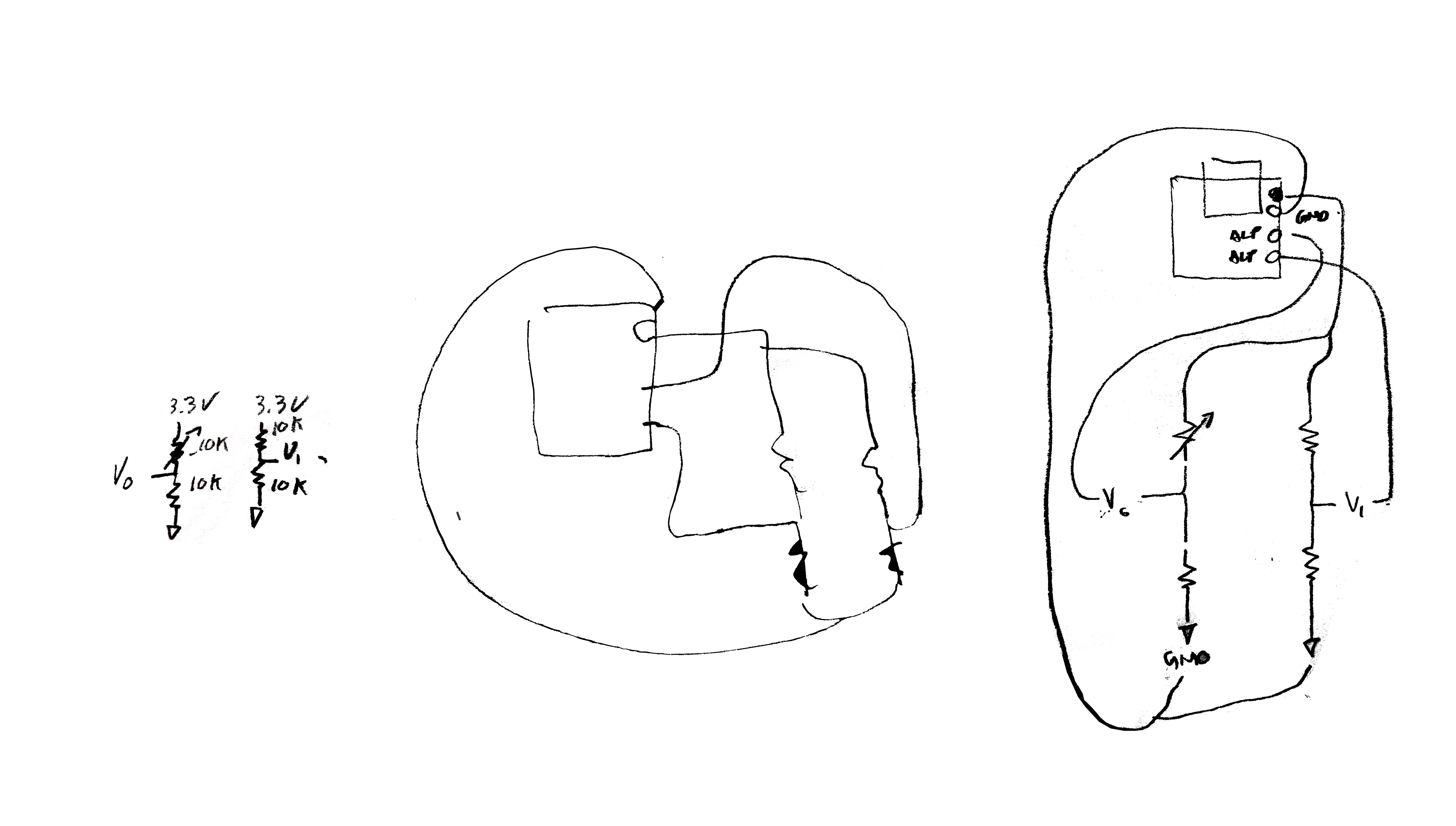
He explained that the schema works by establishing a base with a pair of resistors and measuring the temperature using a second pair of resistors (one of which is a thermistor). He also explained that it should be relatively easy to find a thermistor as MIT has some in stock.
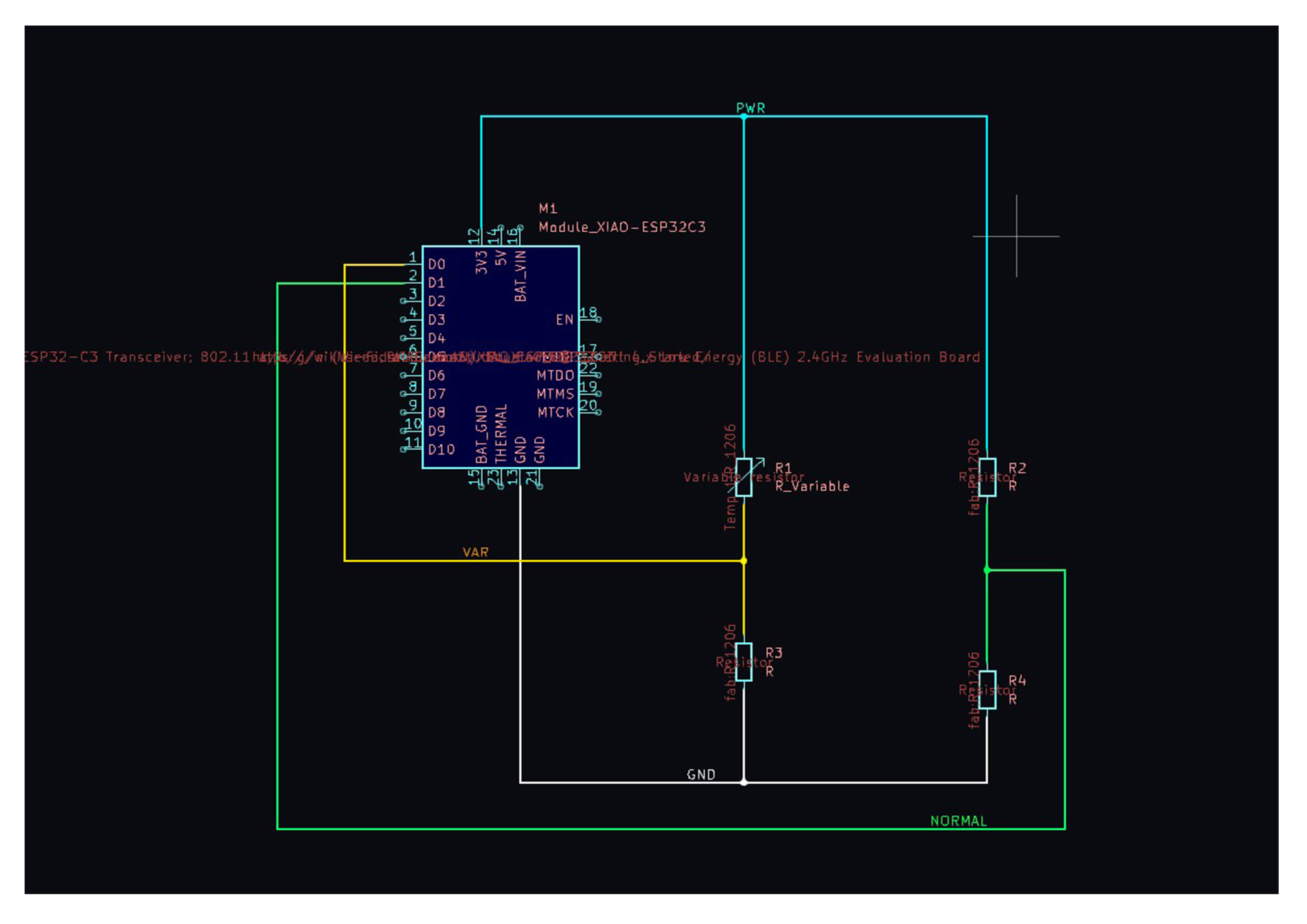
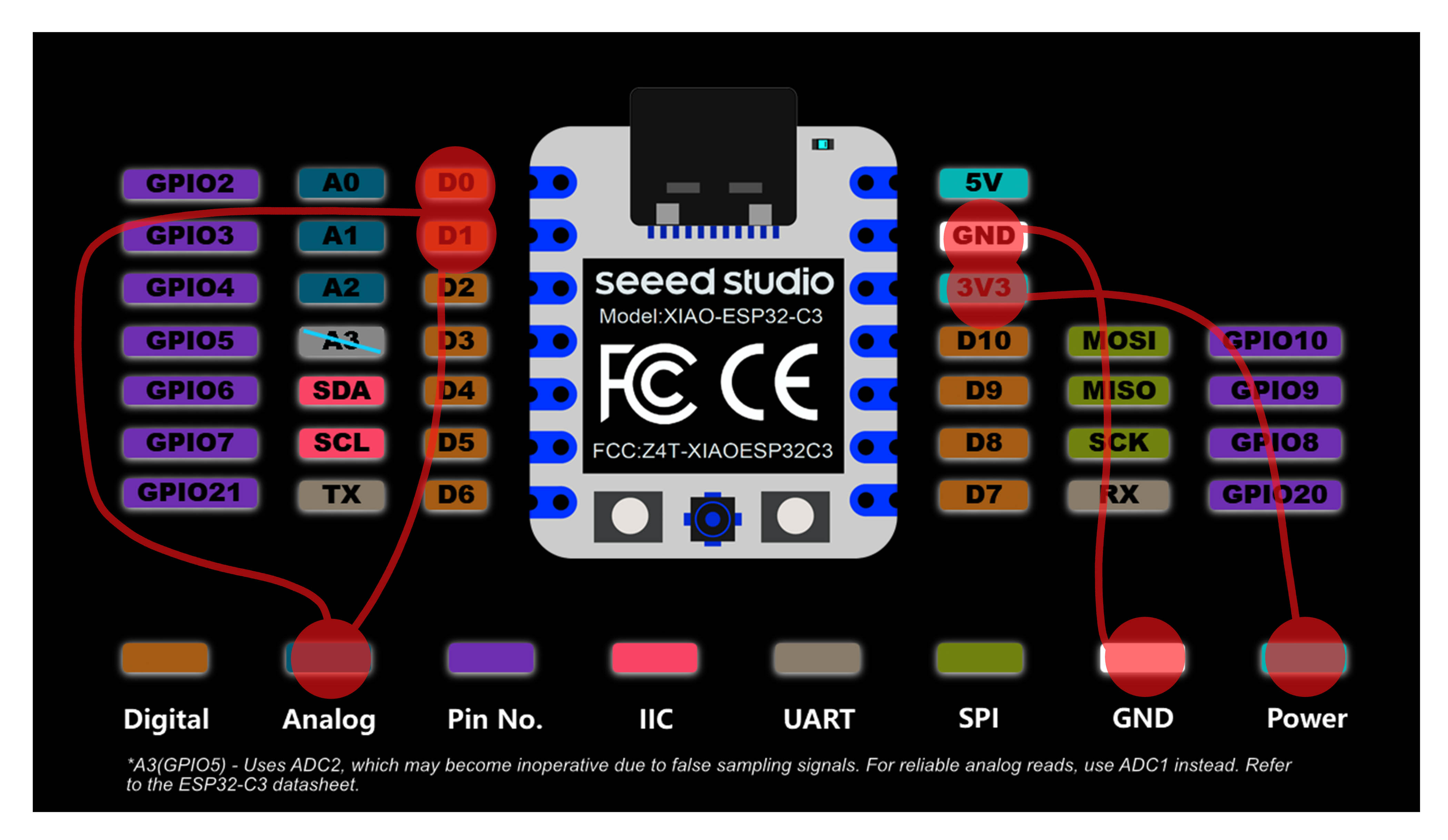
I started by drawing the schema in KiCAD. The two pairs of resistors both connect to ground on one end and to the power output on another end. Between them a signal line extends to analogue pins on the XIAO ESP3 C3. Pin number A0 and A1.
I find that every week there is some kind of hiccup, this week it was with the milling machines. I think my Roland luck had run out by this stage.
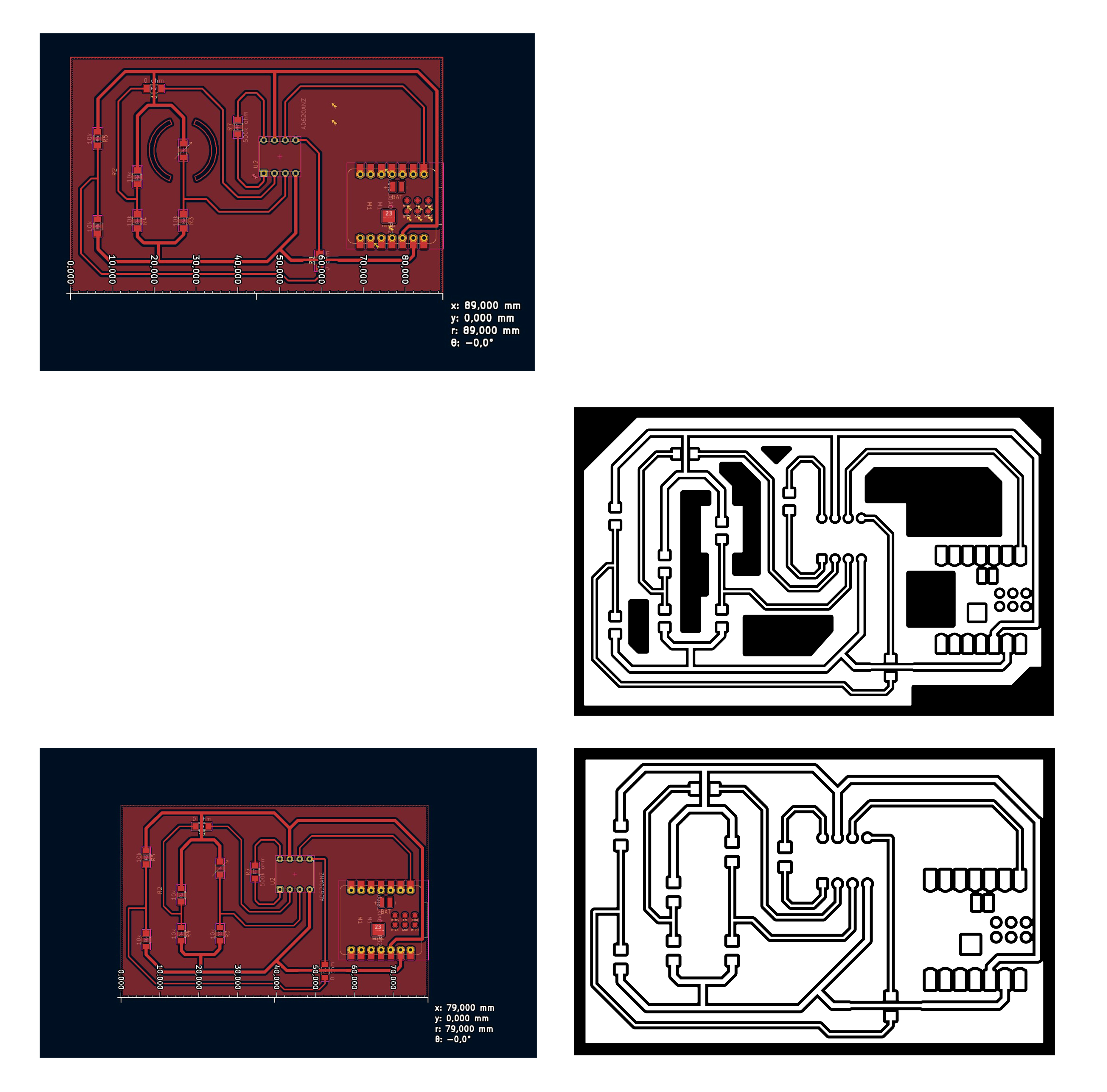
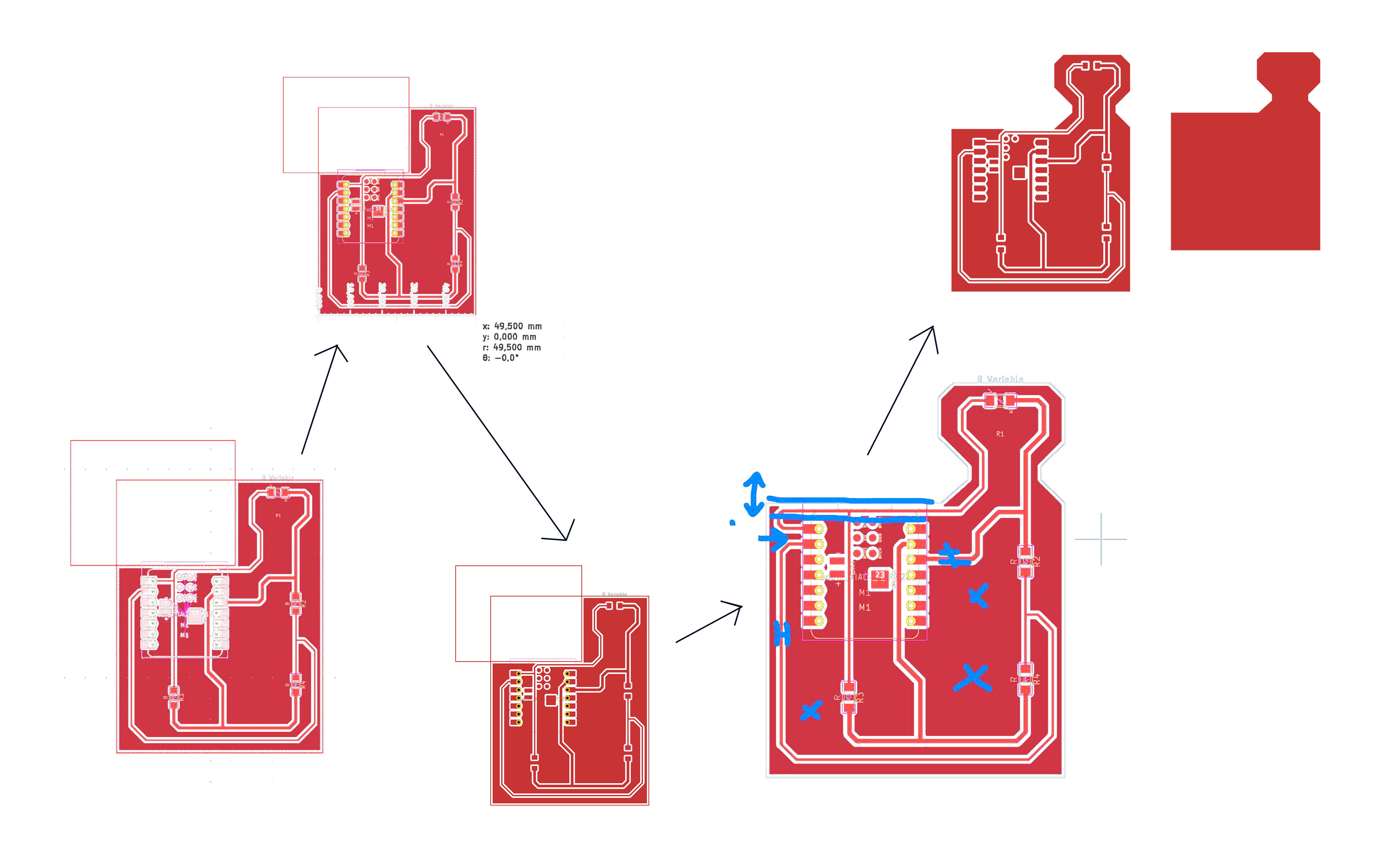
Exporting the PCB schematics went relatively smoothly. I transferred the KiCAD data through Gerbers, by way of fabrication outputs. I ran the relevant Gerber files through Quentin’s Gerber converter to receive PNG files which could be used by the milling machines.
Workflow

Production – Machine Issues
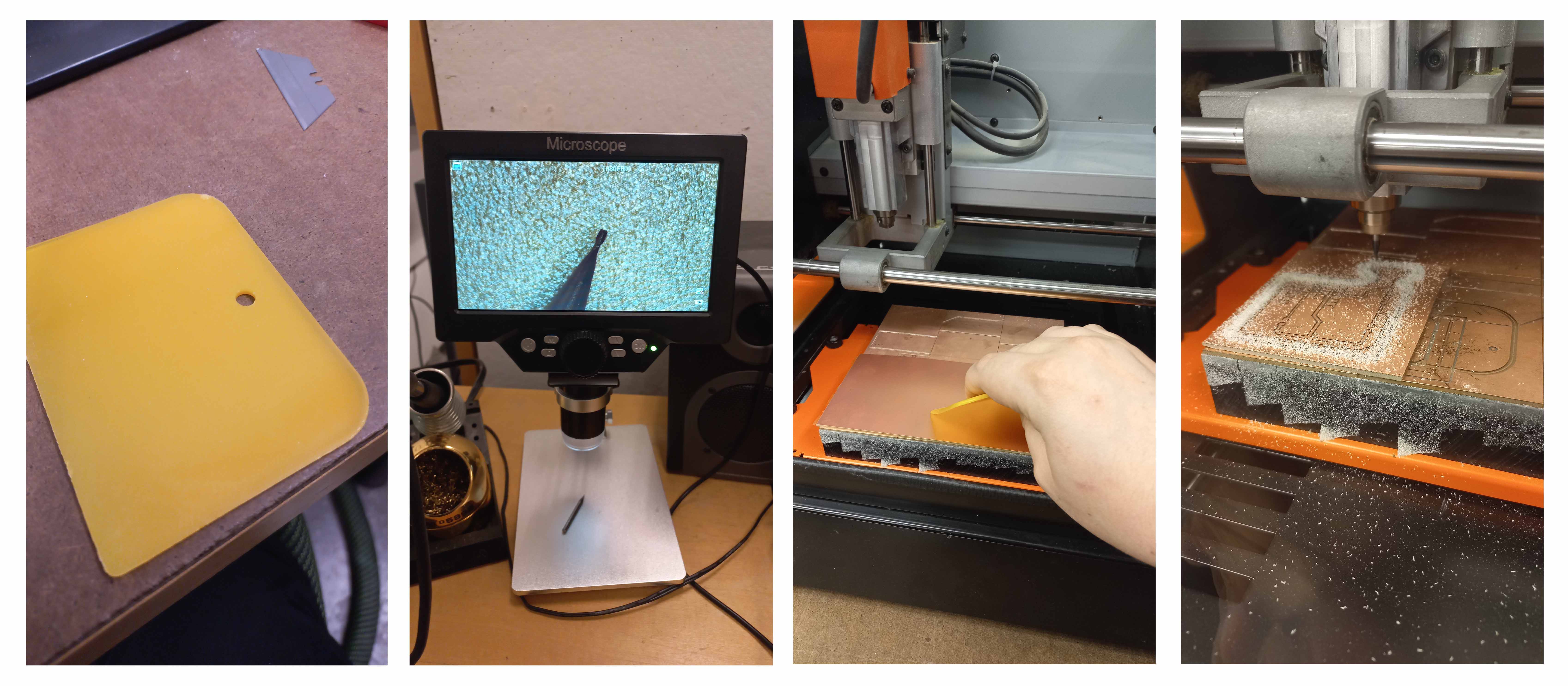
The first section I did on Monday evening where I tried to end the night with some physical PCB production. The tracing went relatively well on the first run through. There were some dodgy connections, but it seemed intact enough for me to continue to the cutting stage. Here something went wrong. The N-mill did not excavate the board coherently and therefore I had to have 5 run-throughs. Each time I increased the ‘cut depth’ value so as to gradually excavate more and more of the outside track. For some reason the machine did a single lap and then 5 laps in the air, almost like it was shadow cutting. Eventually I decided to change the actual N-mill to another 32-bit, and then I cut all the way through.
The following day I decided to simplify the design to avoid possible complications when I mill again. I increased the spacing in front of the XIAO to allow for a thicker signal wire. I routed the route to the A0 pin so that I entered the micro controller from the front and made sure the connections were adequate and thick enough. I also removed the decorative holes so that the machine would only have to cut the borders of the PCB.
Here my problems started.
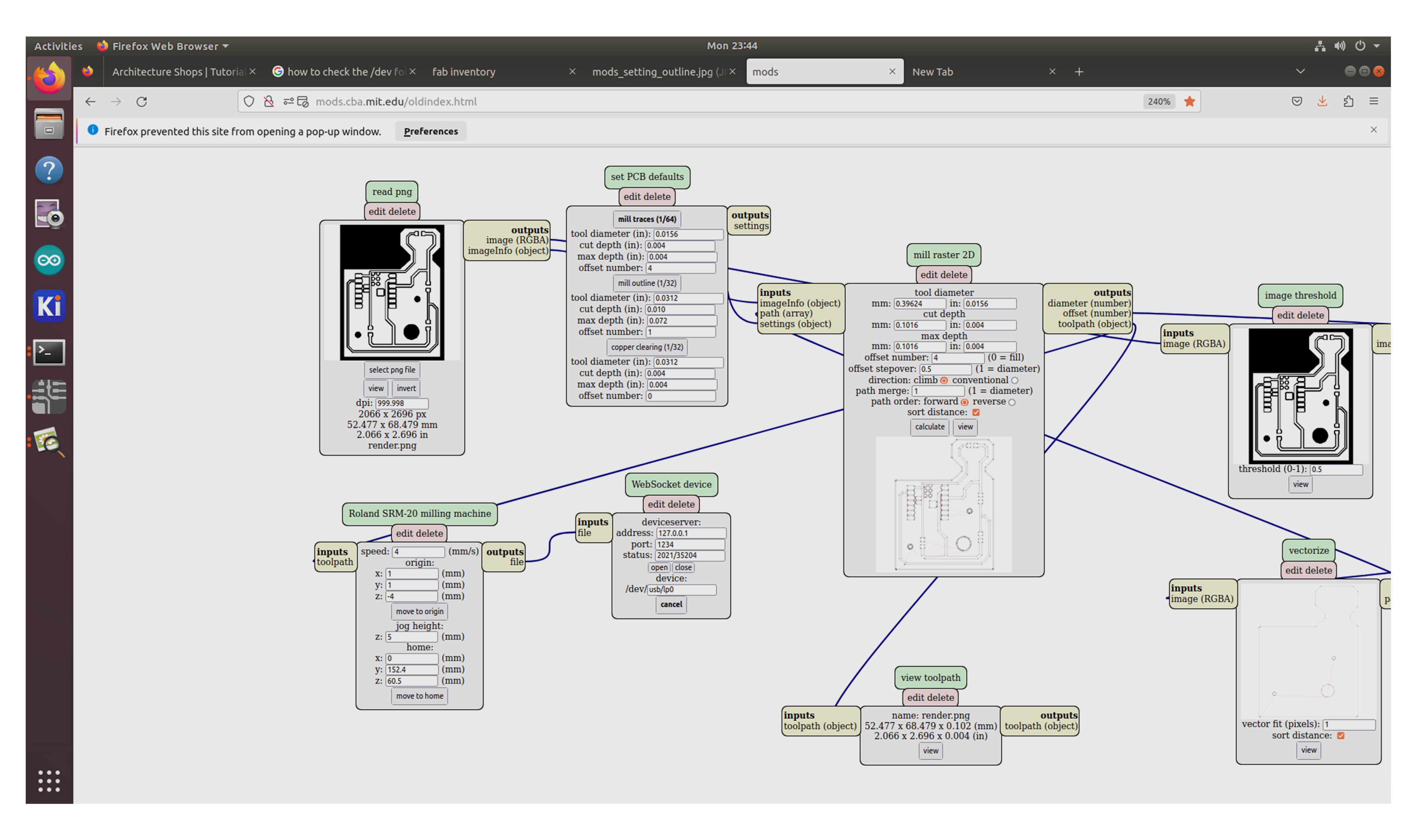
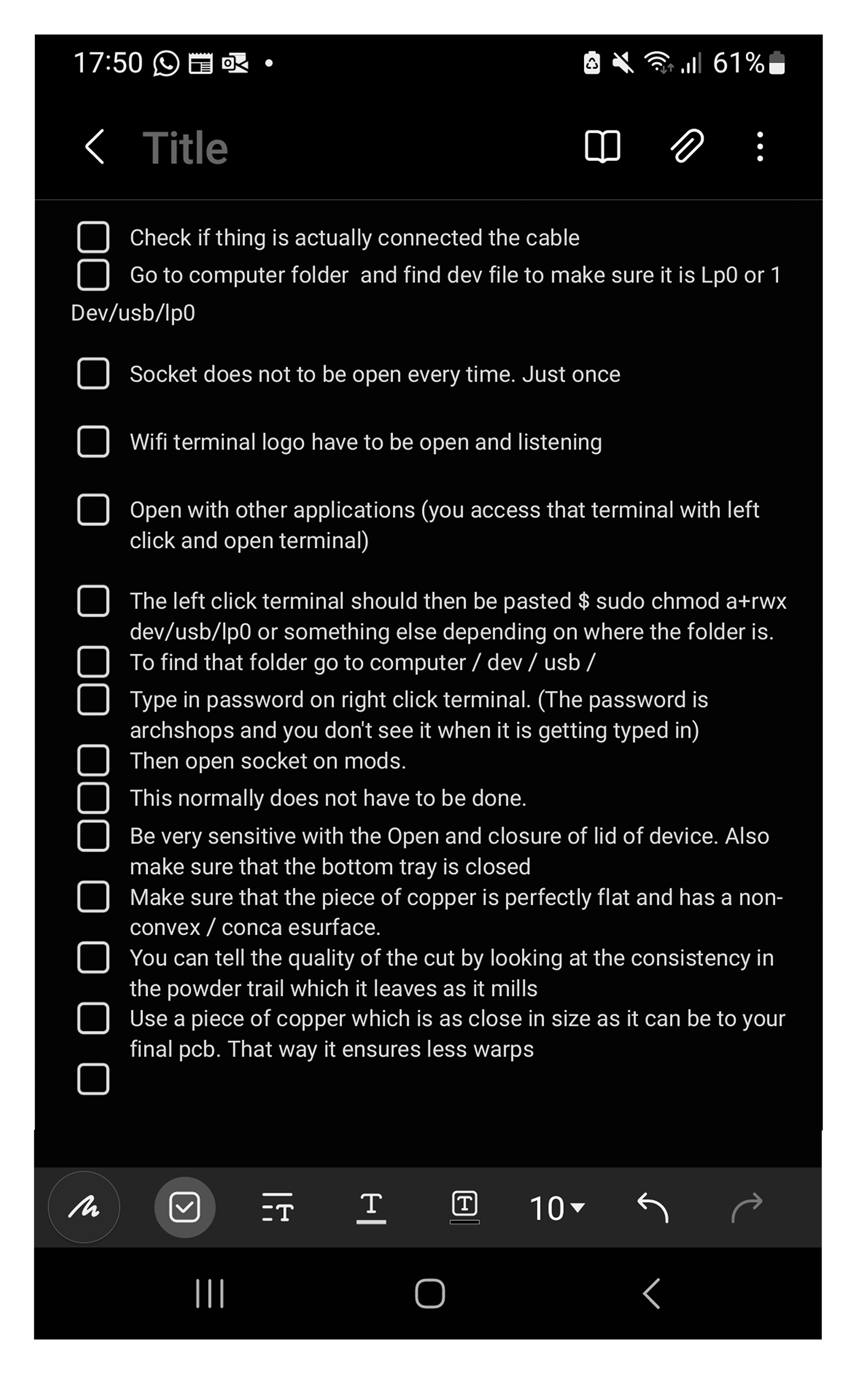
I attempted to start up the Roland SRM-20 and it seemed that it had lost connection to its socket. Jen helped me to reconnect to the Roland and things seemed to be working once again. After my first operation, the light started blinking. It turned out that the problem was 2 pronged. The Roland has a very sensitive door which, when even slightly ajar, will likely cause the operation which you want to execute to stutter. The list on this page details steps which you should follow if you are totally disconnected from the mods page.
Production – Manufacturing Issues
After sorting out the machines, I turned my attention to milling. Like my last round of PCB making it was fraught with issues. Only this time it was physical not design related. I think something which I’ve noticed about my general attitude towards design is that it has shifted. I no longer see failures as failures, but as opportunities to document. I’m going to credit Neil for that one (the change in attitude; not the amount of failures)
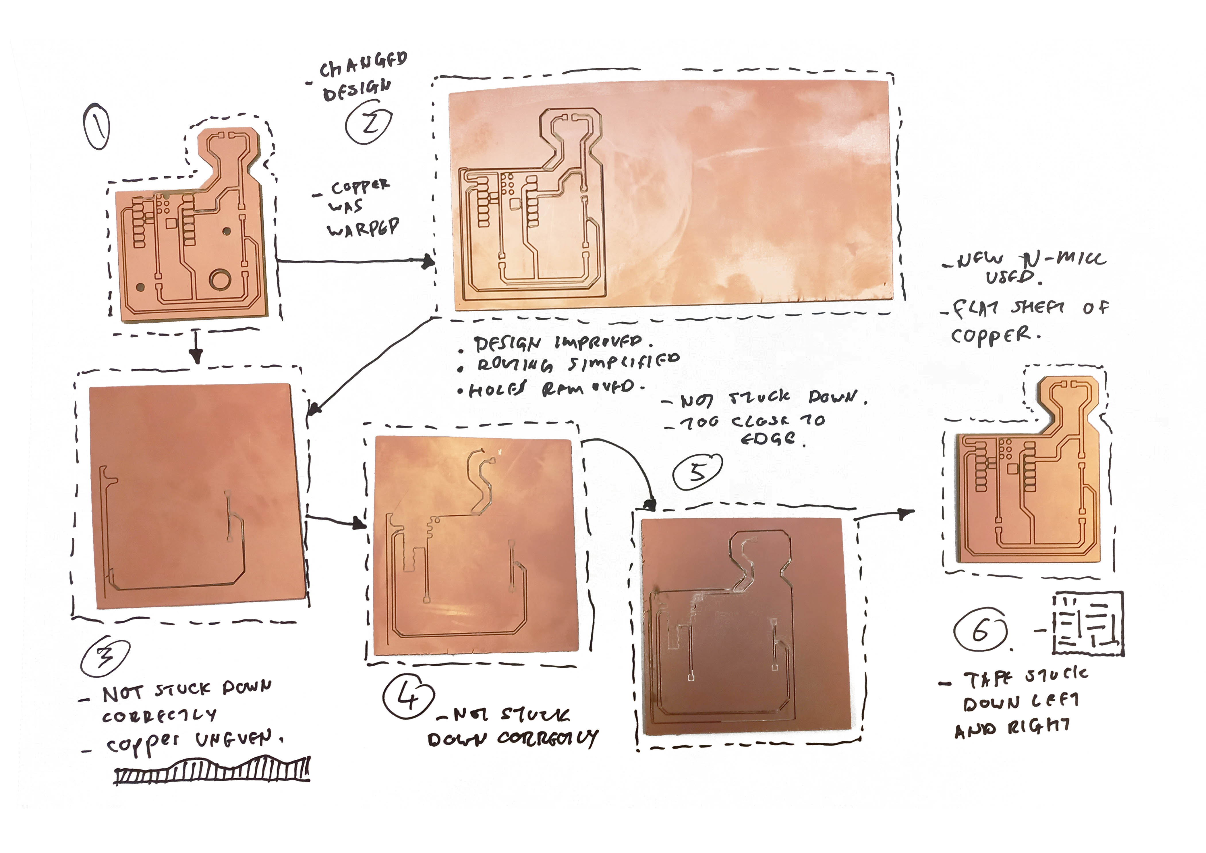
My second board (after the one I did the previous night) failed due to the size of the copper plate. Because it was so large, it tended to warp much more easily. Shah advised me to use a board closer in size to my final product to eliminate a degree of error.
My third, fourth and fifth board, although smaller in size, spun of the milling platform due to the tape not being strong enough, some of the boards were not completely flat on the milling platform and some of them were not completely flat in profile. All of these issues contributed, perhaps in tandem, to the eventual failure.

Production – Succeses
The sixth board was my last straw and if that did not work, I would leave the arch shops determined to find someone who could point me in the direction of adequate material and adequate inventory.
I found a reasonably sized copper plate which seemed flat enough in shape and profile. This time I taped the board in two directions in the x and y-axis so as to generate more resistance to the N-Mill turning in two directions. I had just watched Nate complete a successful board and ‘’though maybe I am the problem not them’. This time I used the new N-mill 64 and 32 bits and that already seemed to deliver positives for Nate.
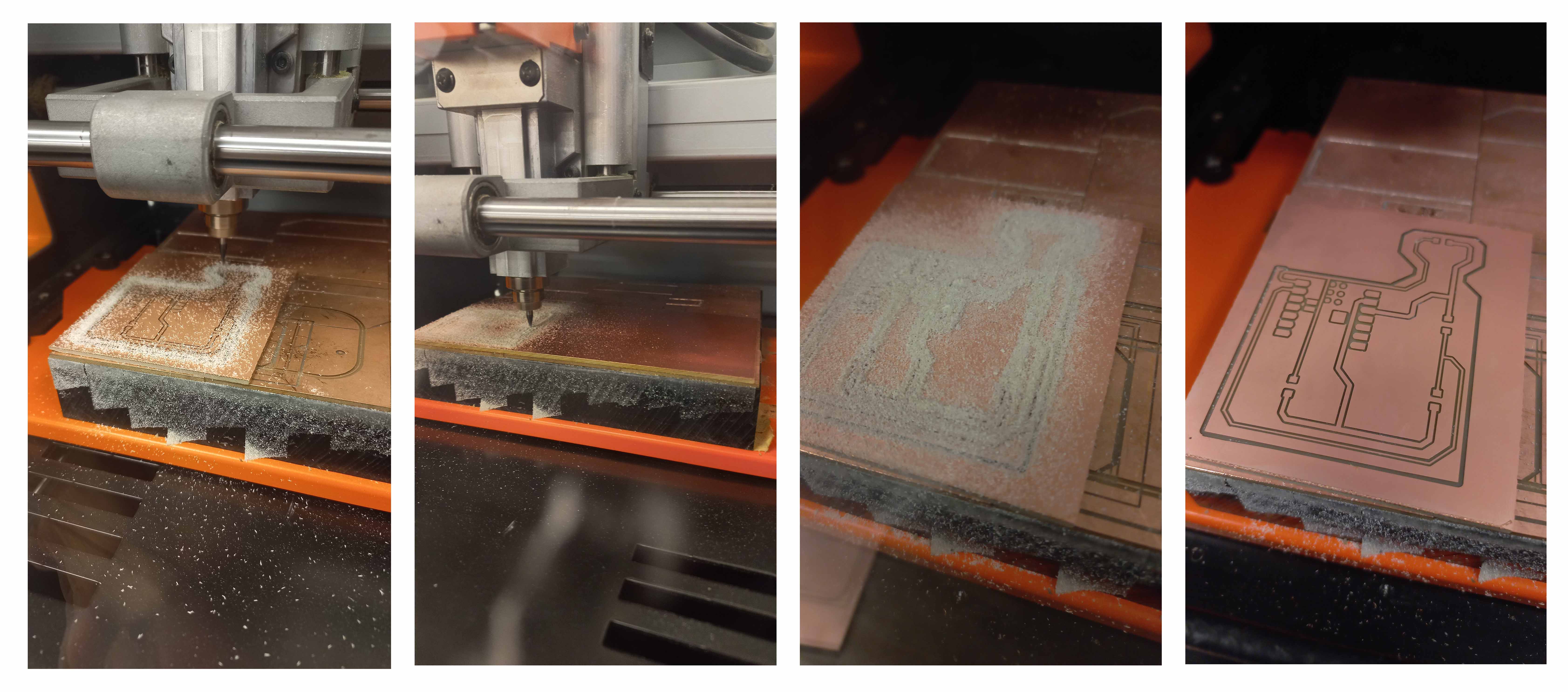
The change in N-Mill and plate delivered promising results. I could tell by the quality and regularity of the powder traces left by the N-Mill that the cuts are clean and precise. After milling was finished, I moved onto soldering.
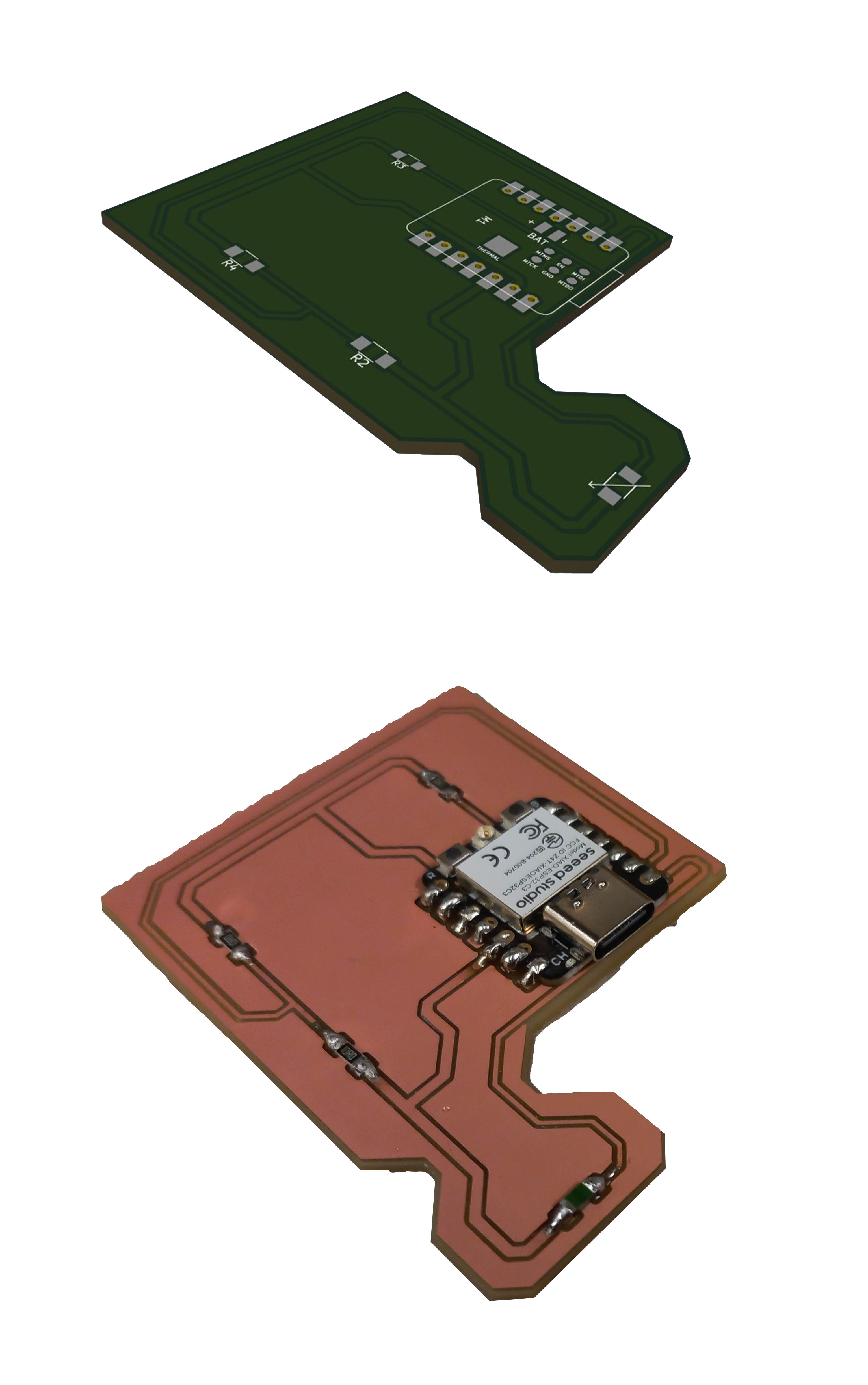
Production – Soldering and Multimeter testing.
Soldering went well, with each iteration I understand the personality of the solder machine and the solder wire better to be able to use it as effectively as possible. It still does require some skill and calmness. Let’s just say that my hands were not made to be a surgeon’s, my patients would all die on the operating table. I applied some left over Capped on tape to the underside of the Xiao. I find that my designs tend to require tracks which ride underneath the surface of the Microcontroller and that placing capped on tape on the underside is good practice. Some other notes which I can leave my future self is to solder structural/ mechanical connections first on the Xiao, and then after you have found your groove, the actual wiring will be more effectively soldered.
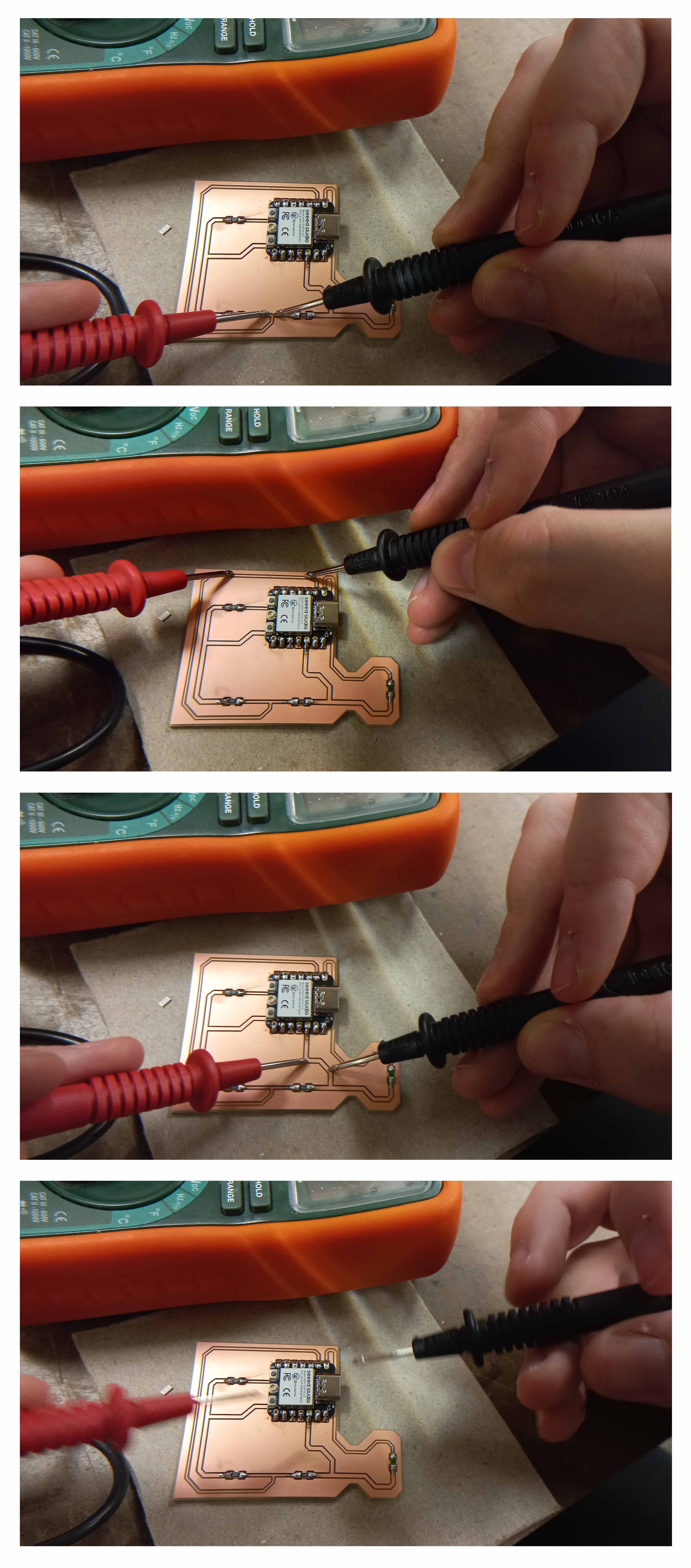
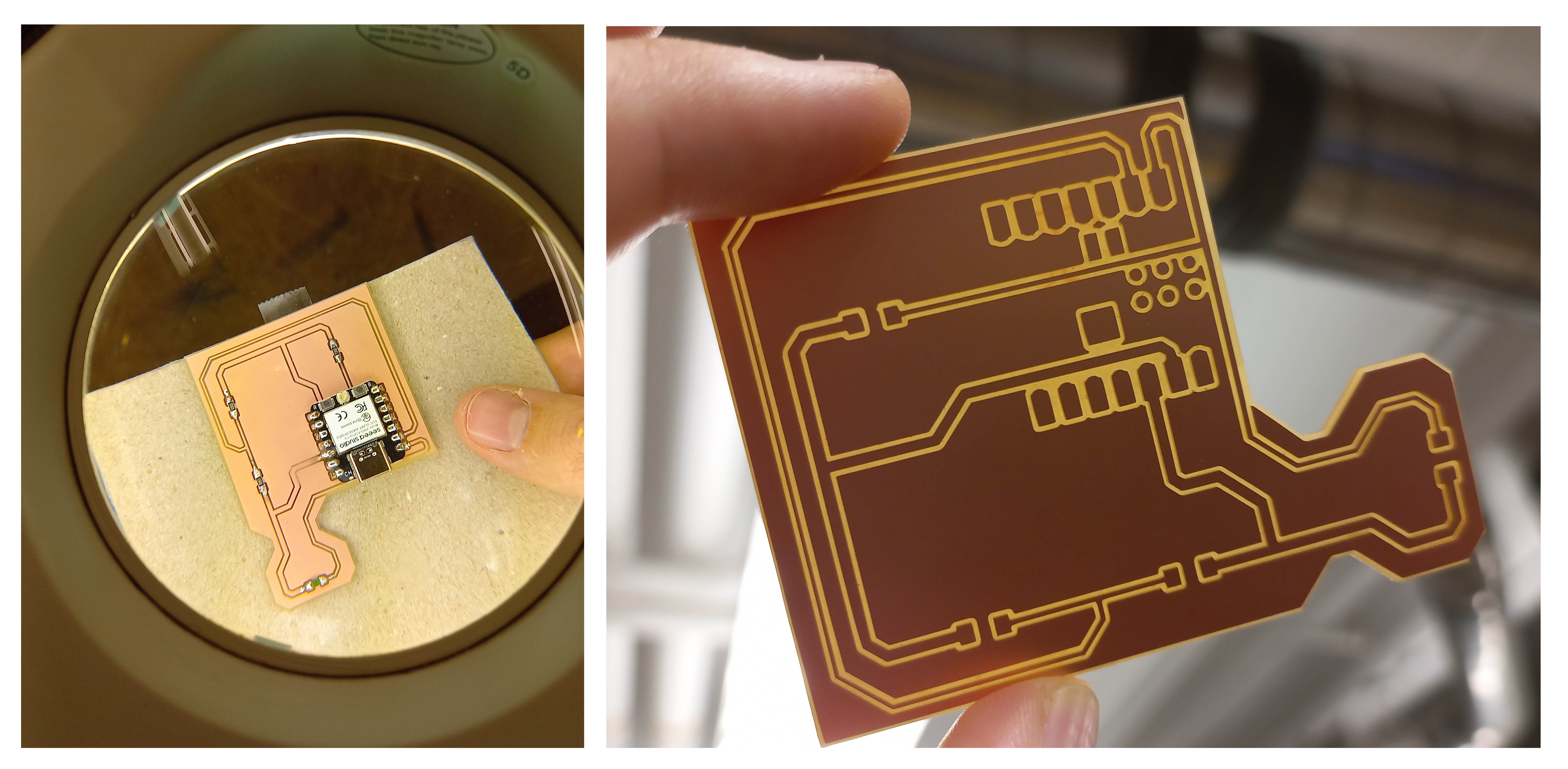
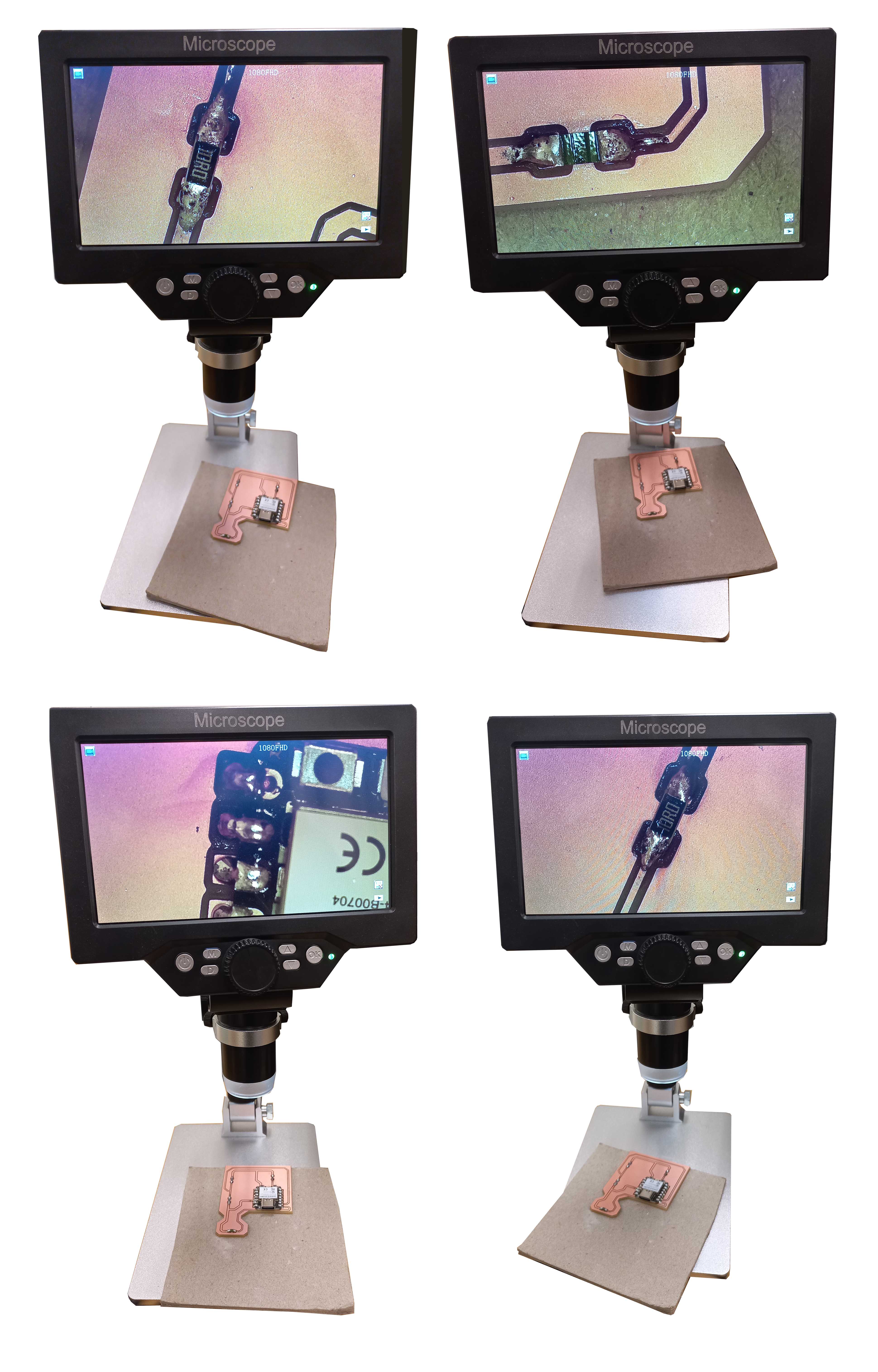
After soldering was finished, I looked at the connections in the magnifying glass under light, under the microscope, and using the multimeter. All the connections seemed isolated and in order.
Coding
I found some code online (most HTMAA students know what that means) and ran it through some checks firstly verifying it and making sure that the pins specified are the same as the ones which the wiring runs to. What helped me is that I did not have to set up Arduino IDE all over again and that I was using the exact same Microcontroller.
I uploaded the code, and it delivered some readings but nothing which made sense. I went back to the Arch Workshops and found the specific thermistor code which was bought of Digi-Key. This narrowed down the search for the Beta value of the thermistor.
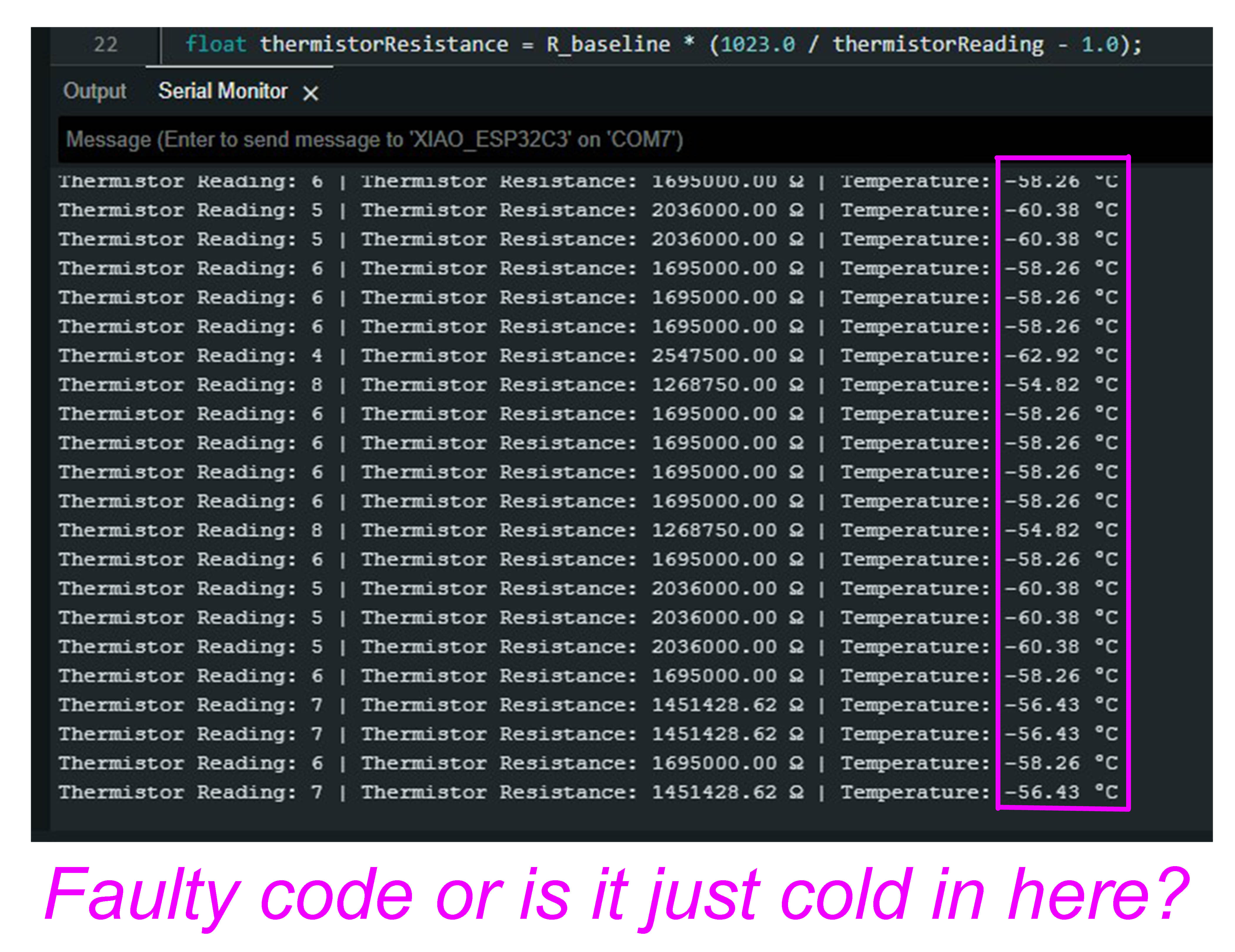
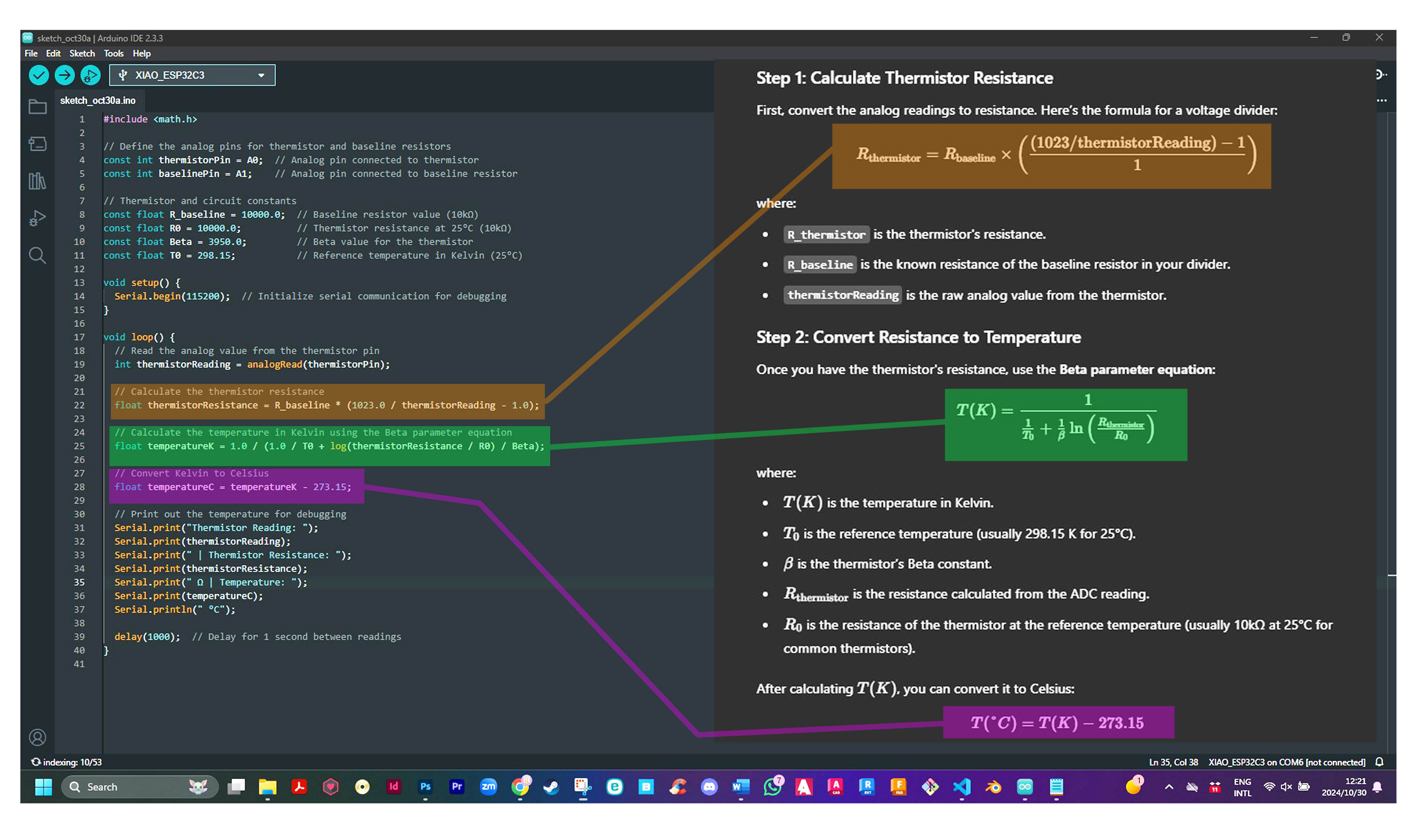
Back to the drawing board
In class, I was lucky enough to be picked by the random generator and then received some expert advice about why my thermal measurer failed. I still didn’t understand completely but I could surmise something of an answer. In class, Neil had drawn a Wheatstone bridge which connected the V1 and V2 outputs to an amplifier which led to one pin on the C3. A Wheatstone bridge is a diamond configuration of two sets of resistors. One of the pairs contains an unknown resistance value. This Wheatstone bridge is then used to calculate the variable.
Because the two input signals were meeting the C3, and because the variation in the two resistors were so small, and because those values would be individually multiplied and then subtracted to generate a temperature value, the resulting value on my initial design would be inaccurate.
The new design incorporated an instrumental amplifier, connected to a third set of resistors from which the final temperature could be offset
Gain = 1 + 50 000 / R g
V out = G (V1 – V2) + V offset.
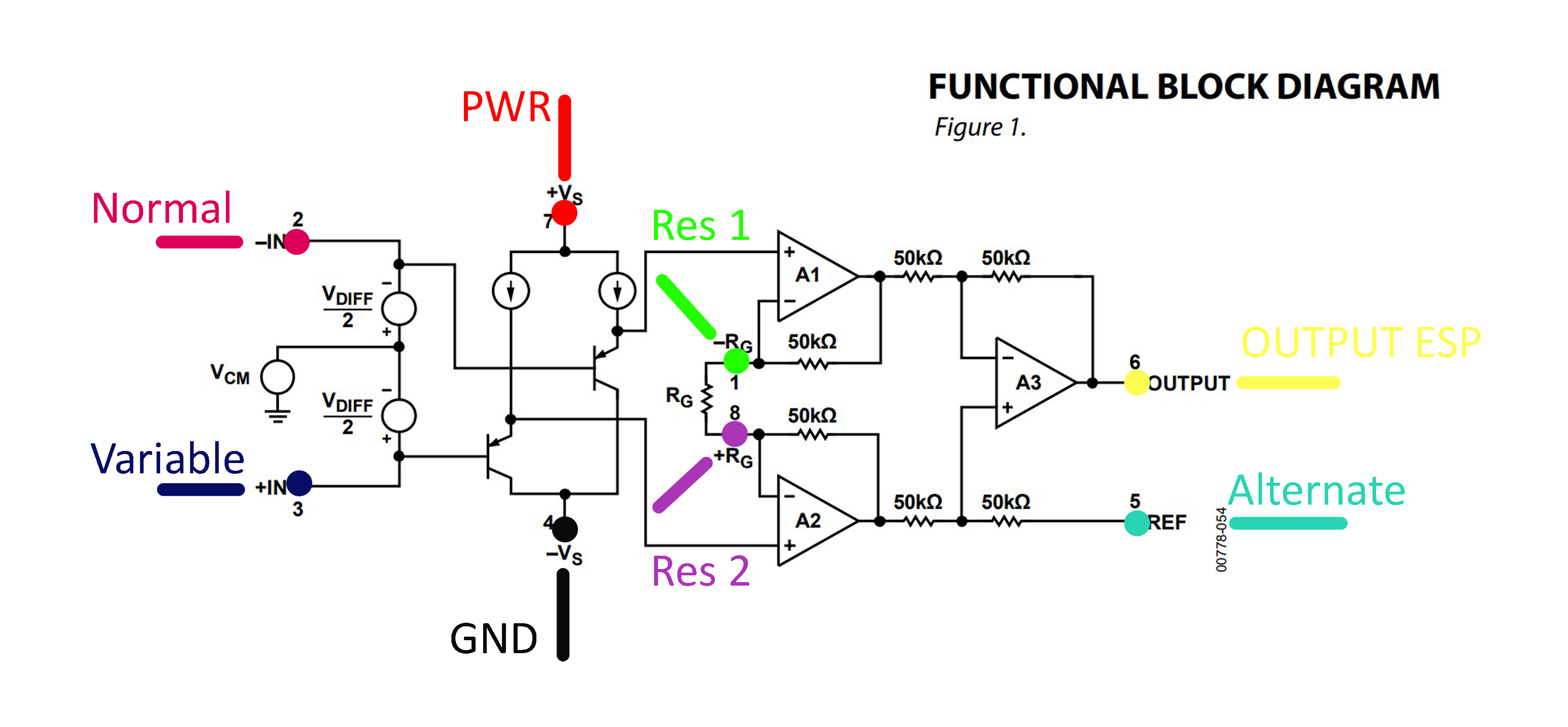
The instrumental amplifier also has a 500k ohm resistor attached to it on both ends in a closed loop. These Rg ports set the overall gain of the resistor.
It seems like a ritual at this point but once again I have landed on compatibility issues regarding the KiCAD footprint files and class reference points not matching up completely. I found, after consultation, that the MAX98357AETE+T amplifier could be used. The problem came in that the KiCAD symbol file and footprint file did not match up. The symbol file had 8 pins and the footprint file had 16 pins.
Back to the back drawing board
Apon further investigation and many more hours of struggling, I realised that the when I spoke to Anthony and consulted about both my Input and Output weeks, (both which involve amplifiers), I accidently confused the MAX98357AETE+T, for the AD620 Low cost low power instrumentation amplifier. I was met by some chuckles in the EECS workshop and knew that I wasn’t the only person who ever which this had happened to. I was suffering inside though.
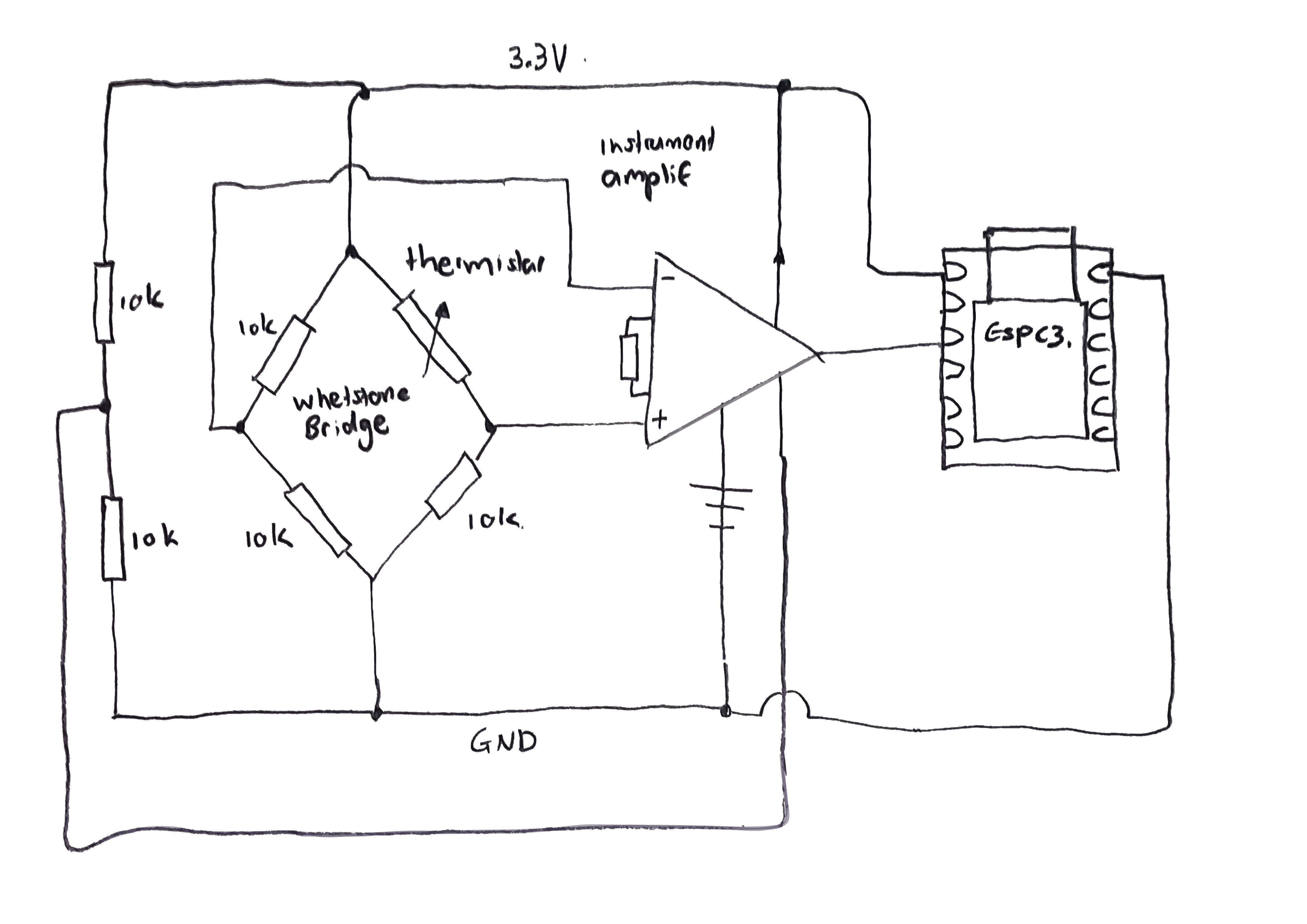
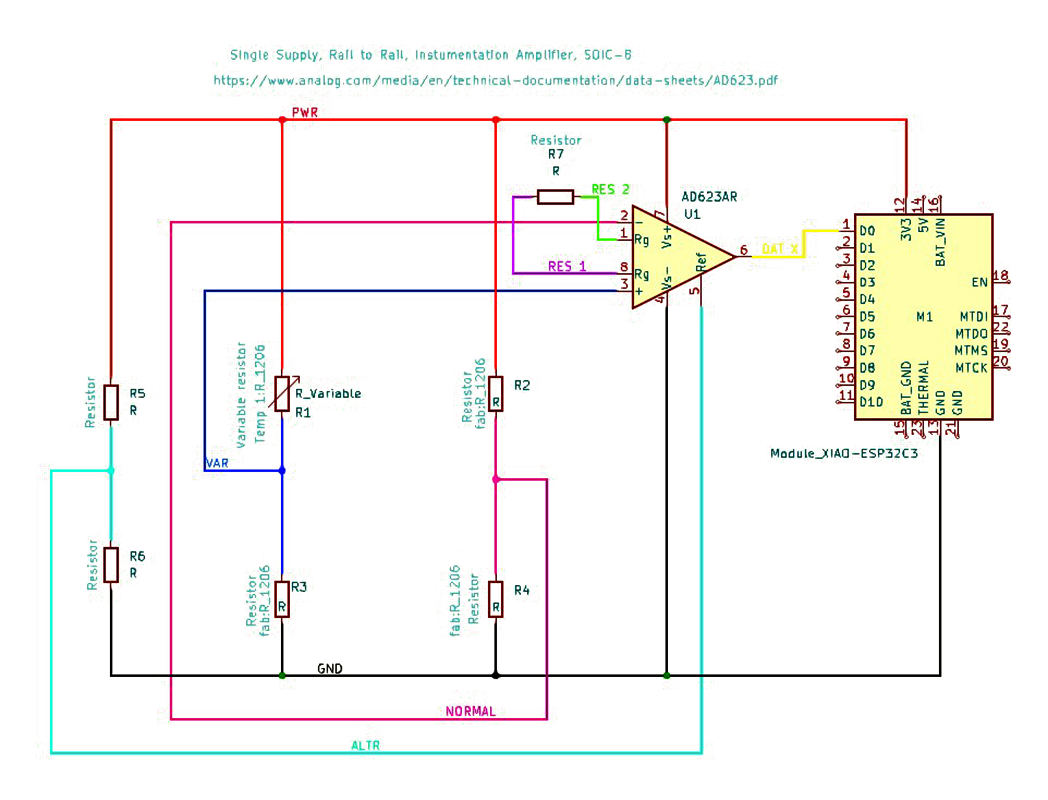
The design went much smoother after this point, and I managed to draw two types of schematics. Both resolved but the second was optimized and made more compact because I realized that there wasn’t large enough copper plates left in the lab. For this schematic I used 0 ohm resistors to bridge across routings in the plate (with the long term success of this yet to be determined)
