Electronics Design
In my pursuit of designing a thermal camera. I have come across the schematics of someone who designed the camera for very cheap. Under $50 they say. Some might call me mad when I say that I am trying to understand this device through drawings, but as an architect this is how I do things.
This week we started off by trying to understand the tools we would be using to debug our electronics, which will almost inevitably become a thing which we would have to do. The reason for debugging is to try and find what is at fault with your work – weather it be a mechanical issue like incorrect soldering, PCB manufacturing errors or other things which I have yet to fail at. Issues which are electronic in nature can relate to code or closely relates to mechanics.
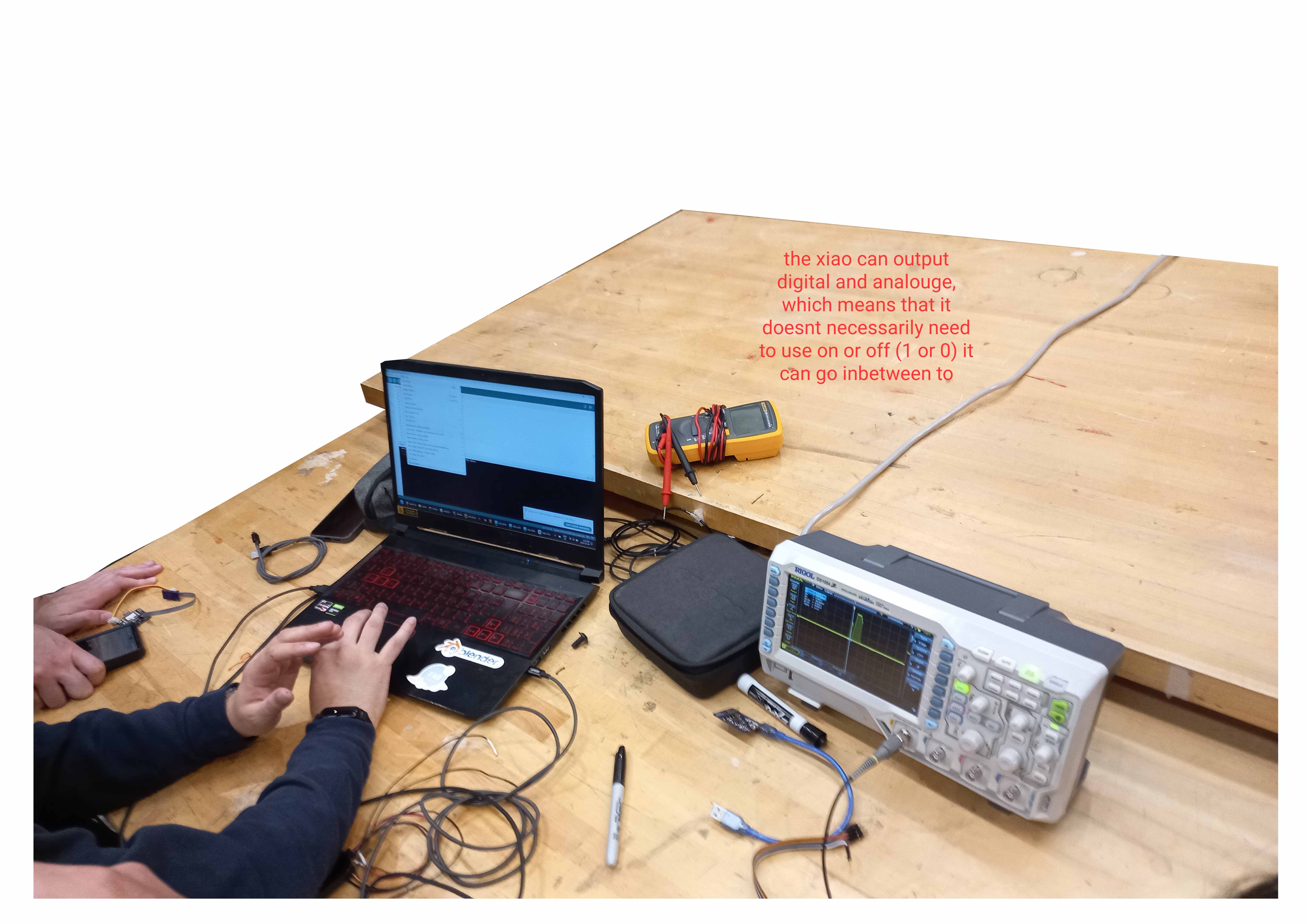
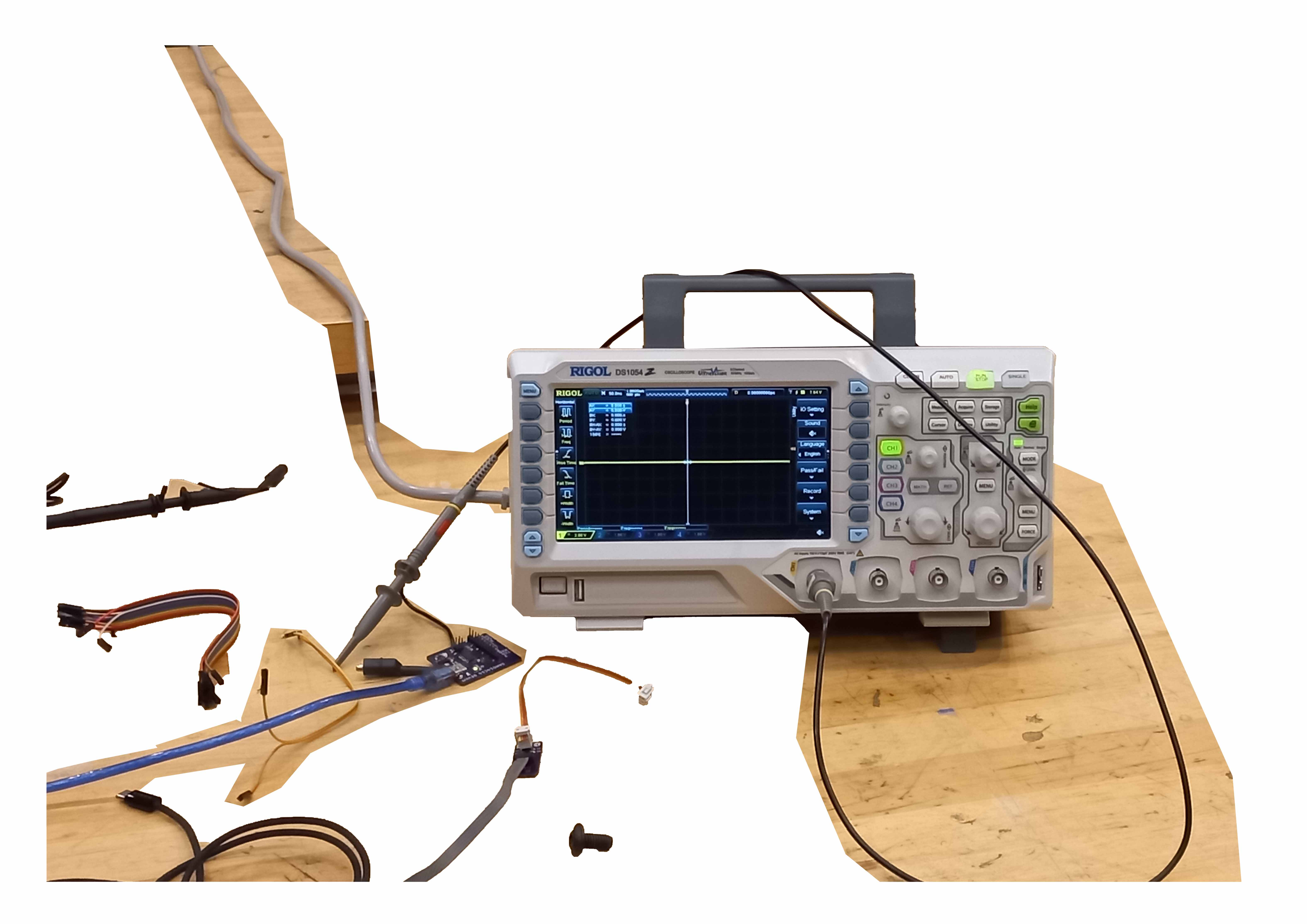
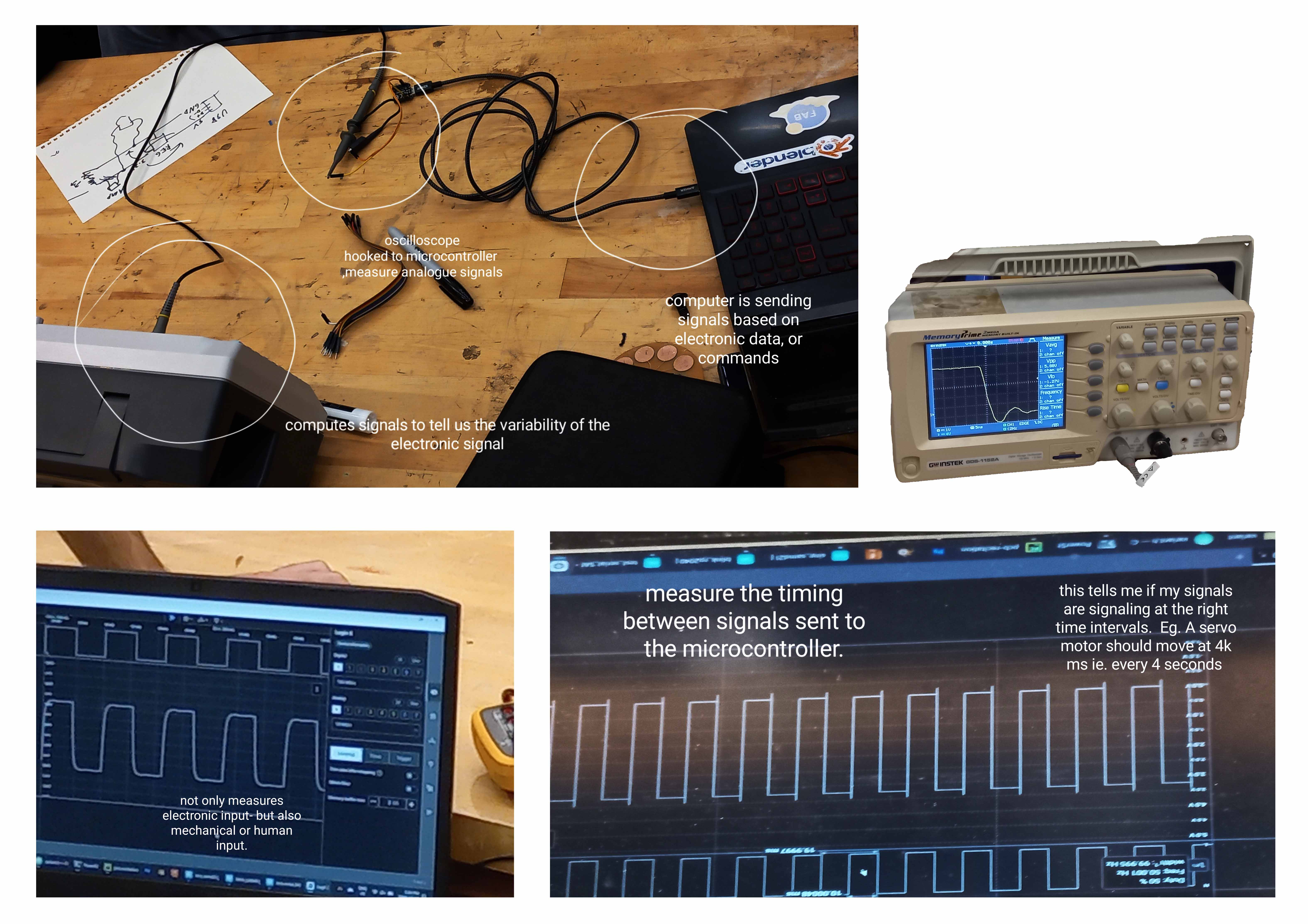
In the group assignment we watched Quentin use the Multimeter (an item which can read voltage, ampere or resistance), the Oscilloscope (a device) which can read voltage difference over time, thus giving the debugger a deeper understanding of the fluctuations within the voltage of a system and another implement which allows us to view digital fluctuations (the oscilloscope being analogue).
Reflection
I learnt that voltage can be negative or positive depending on the directionality of the black and red measurement stick. Also, that a change in voltage can also relate to the commands or codes which we tell an item to do, and in understanding this, we can see if an item is functioning correctly.
For example, if I code a servo motor to move at 4000ms intervals, this will show up on the digital or oscilloscope as spikes every 4000ms. The oscilloscope also measures human input and can fluctuate depending on a human’s interaction with a device (for example a spike when a human presses a button and let’s go of the button.
Workflow

If I was going to try and understand how the PCB board was made, I had to take a step back. I had already drawn the components on paper and connected them on photoshop, but this told me nothing about the actual sizing of the components.
The next step was going to be to see how compact I can make the wiring in KiCAD. Although this week’s exercise might not result in a PCB for the eventual design, it might lead me further down the path and closer to the goal. I am essentially working towards the middle with the final product as an example and my own understanding as a starting point.
To see how small I can make the PCB board I decided to move around the components to see how they relate, and which configuration might be the most optimal.
Much like in architecture, by redrawing things you start to understand individual components and the greater scheme much better. I understand that I do not yet have all the answers to accurately understand how this system functions, at this stage I need to be able to ask accurate and the correct questions.
Firstly, I was trying to understand my role in the design, to try and separate component from design and PCB. By studying the existing PCB boards, I learnt that GND points are not necessarily connected to one another, however they need the same voltage to act as a baseline for the rest of the system. I also learnt how KiCAD functions, however I have yet to master it. I associated the Schematic symbols to their footprints manually because the components were not necessarily available at MIT or otherwise locally.
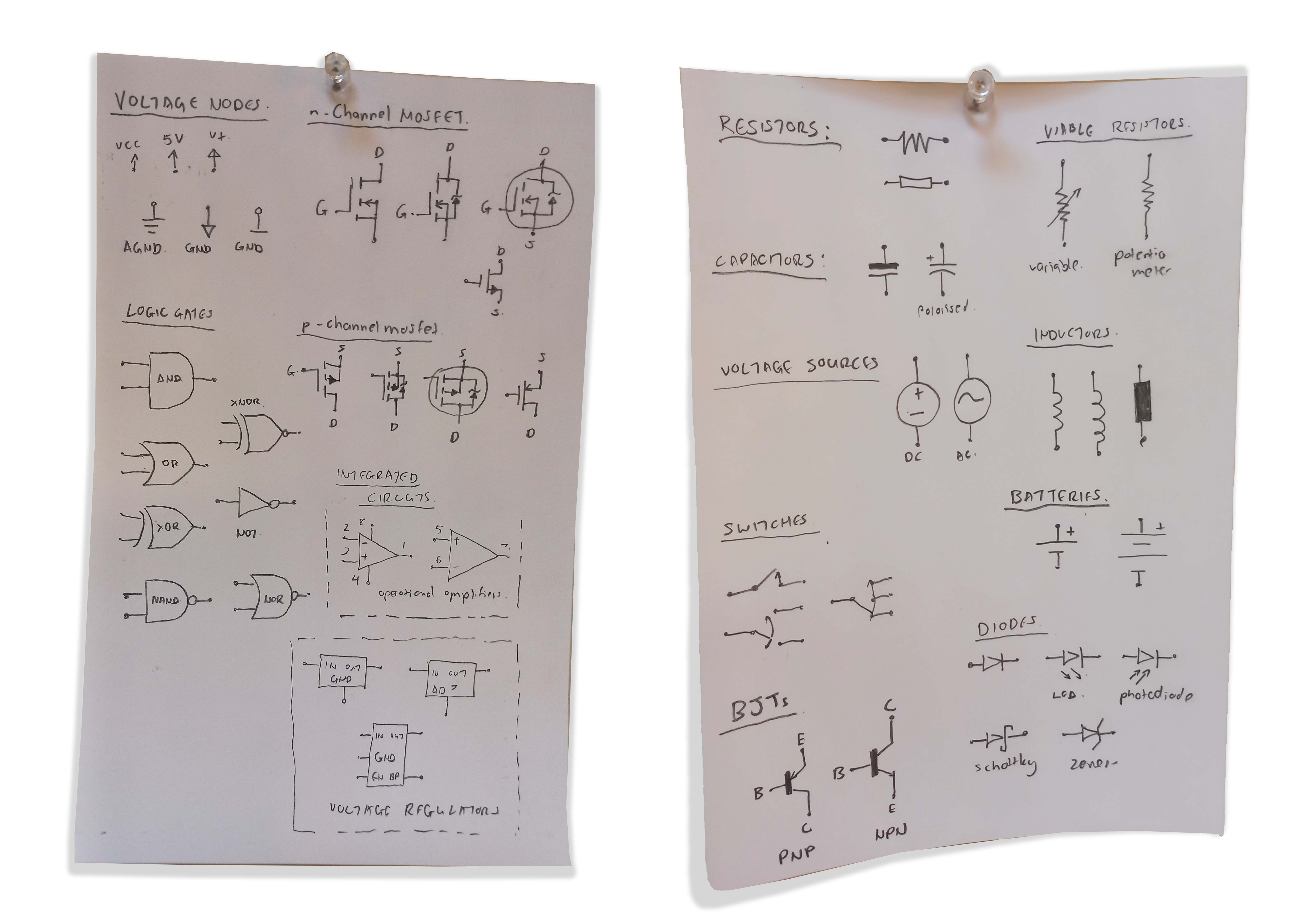
My initial attempts at recollecting my very limited memory of electronic design. I did this to form a lexicon for the purpose of reading the existing electronic schematics. This was going to be my Rosetta stone.
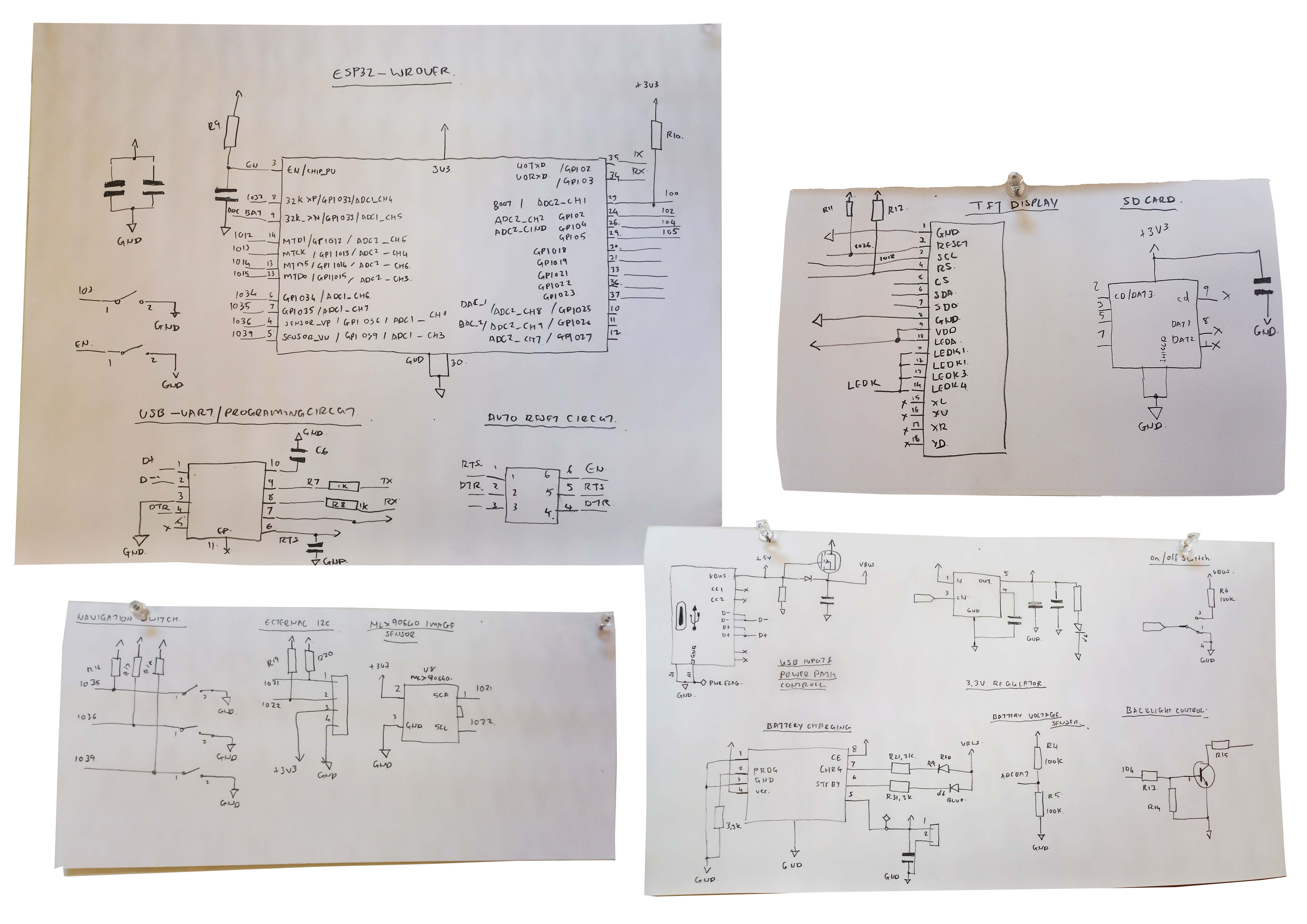
What I discovered when I redrew the images the first time is that each wire number corresponds to the correct port in of a different component. This gave me a vague understanding of the relationship between some of the components.
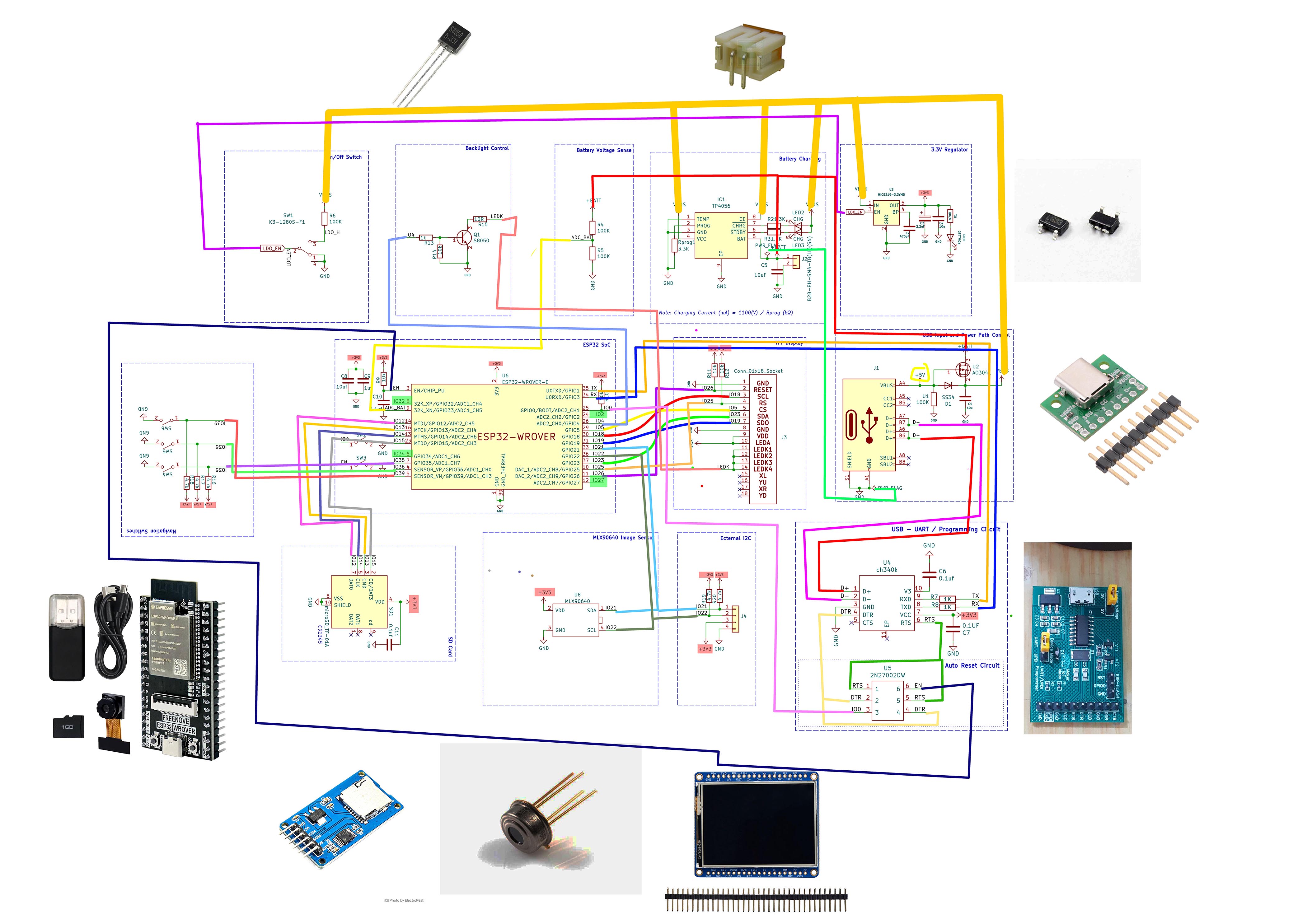
With this image I was trying to understand the functionality of the system. I started off by arranging the components according to how the user might use the device, and to keep the wiring as simple and efficient as possible. In essence I was simultaneously trying to become more confident in my understanding of the relationship and importance of each piece of electronics.
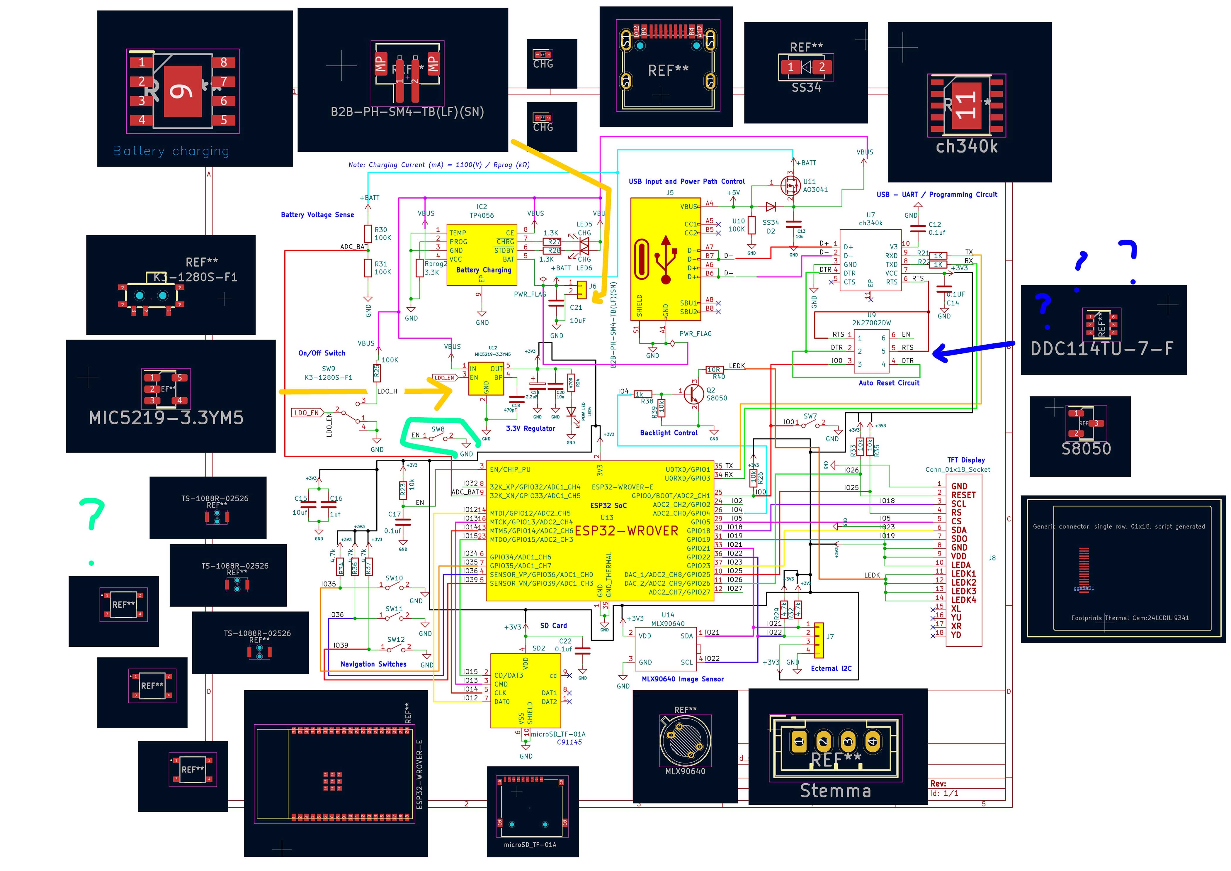
This previous step helped me when I repeated the connections in KiCAD (so to eventually try and optimize the design). Understanding the interface of the program was relative to manage as this is my first time using this program. I am also trying to understand the scale of the electronics so as to know if adjacent wiring will interfere with each other or have enough space to properly function.
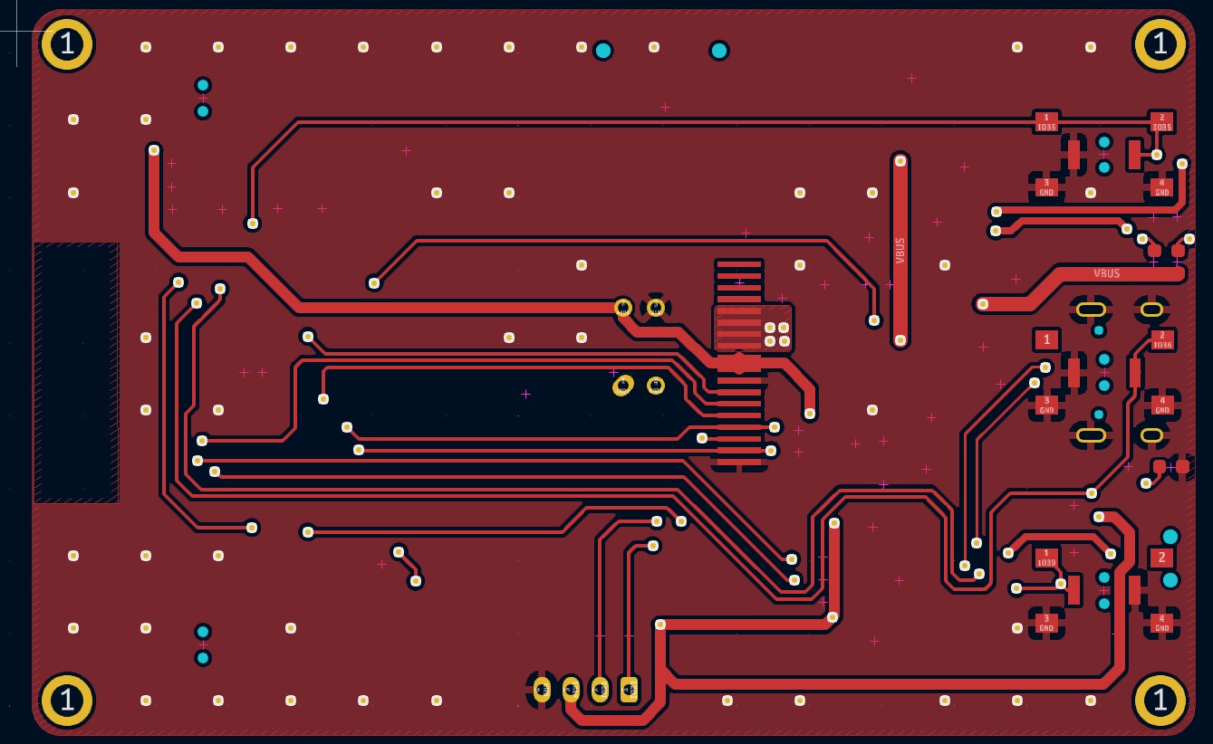
At this stage I gave up (for now) trying to produce a fully reproducible PCB board for the thermal camera. Instead, I tried focusing on what the lines mean (yes, I am at that stage). How the components relate to the wiring, and to what extent I can use KiCAD to try and simplify my workflow.
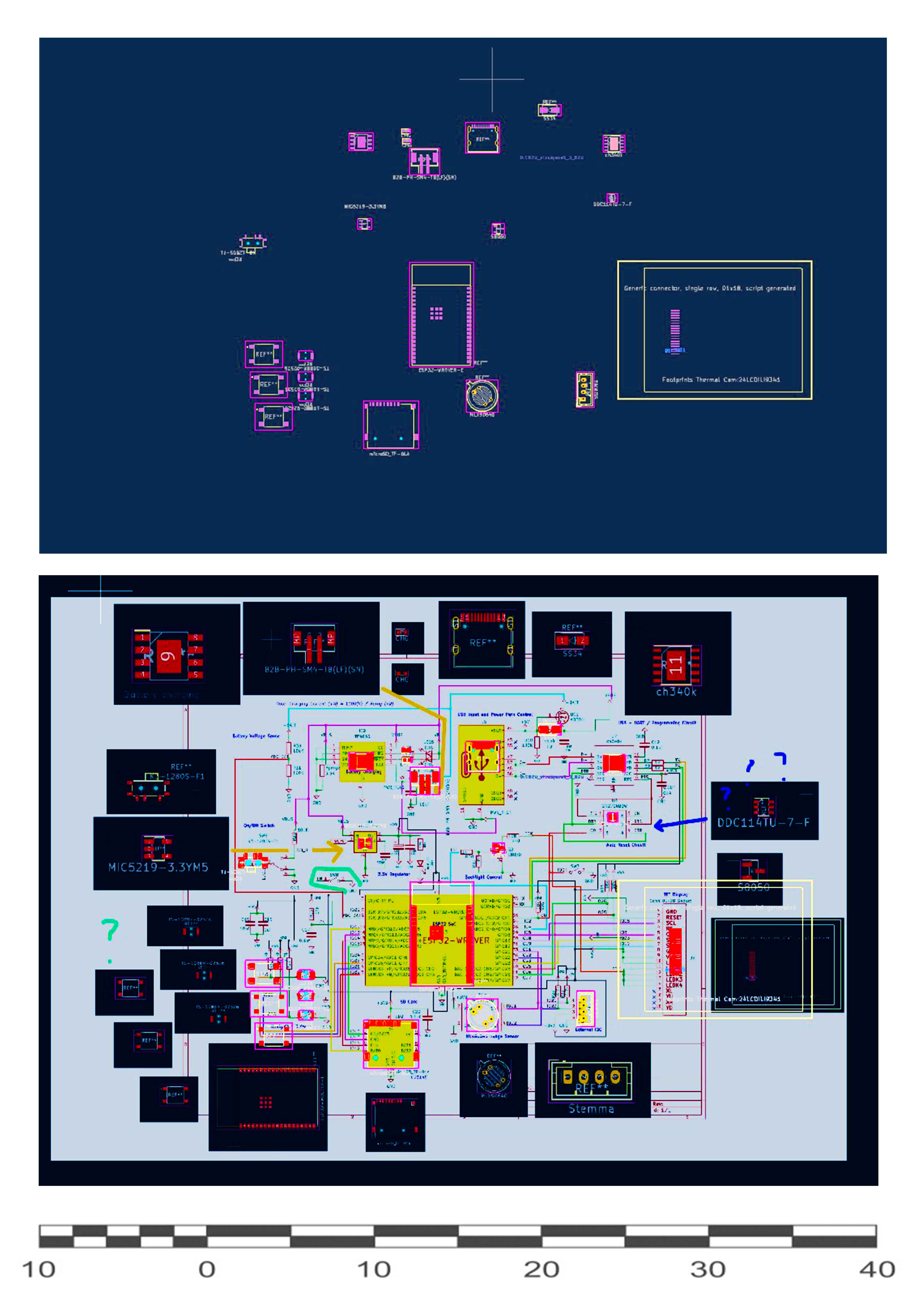
The actual sizes of the components placed up to the wiring diagram, this shows the space for optimization in sizing of the components and gives you a better idea of what the eventual scheme will be like when the PCB is produced.
Group Project
