Electronics Manufacturing
This week we were tasked with producing our PCB boards. I had some questions regarding my previous design which Anthony helped me with. These questions and answers gave me some further insight into the inner workings of the eventual project which aims to design a thermal camera.
Reflection
I discovered that the TX and RX connections need to be cross connected as they communicate and respond to one another. Secondly, my design can be simplified by removing more than half of the components! This can be achieved due to the built-in capabilities of the Xiao ESP32. Thirdly I learnt that the Ground connection can be a cable in the form of a larger and thicker plane. Routings which carry current also need to be thicker to be able to handle larger voltages.
Workflow

Program learning and KICAD
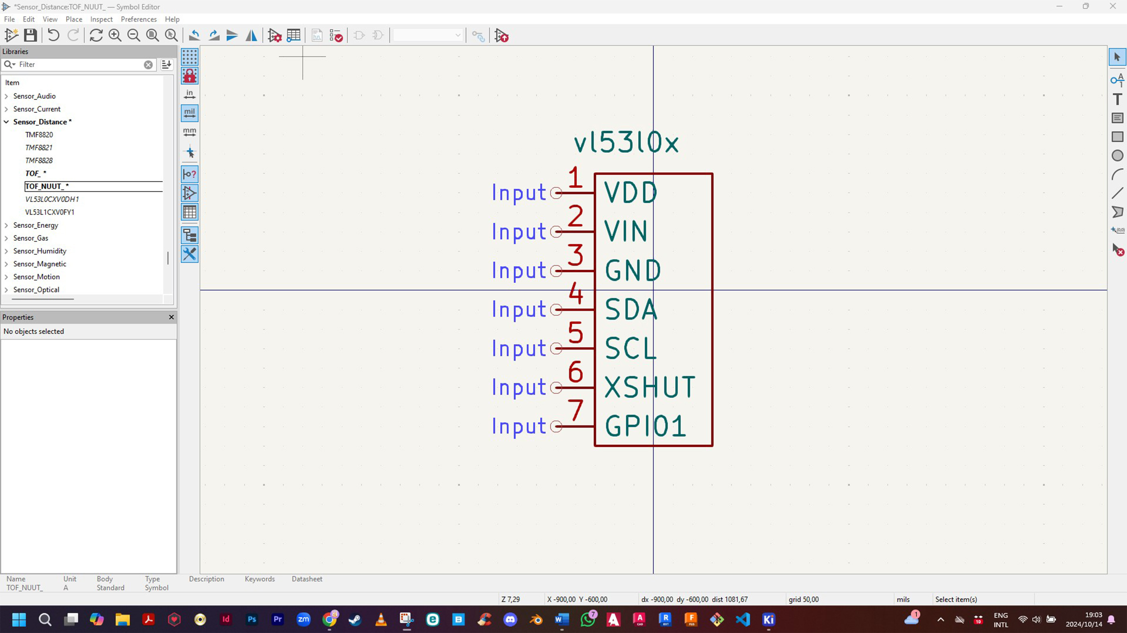
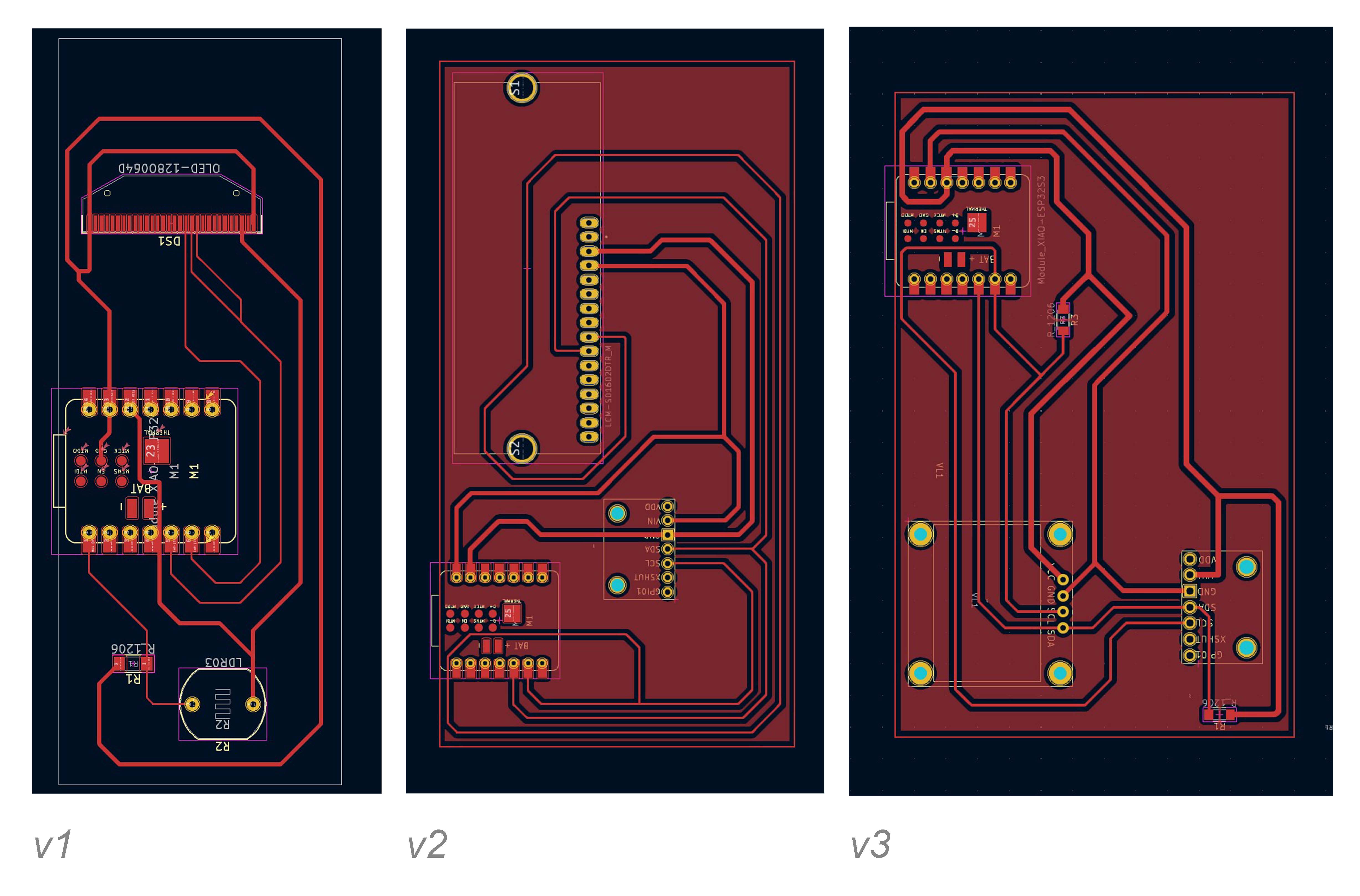
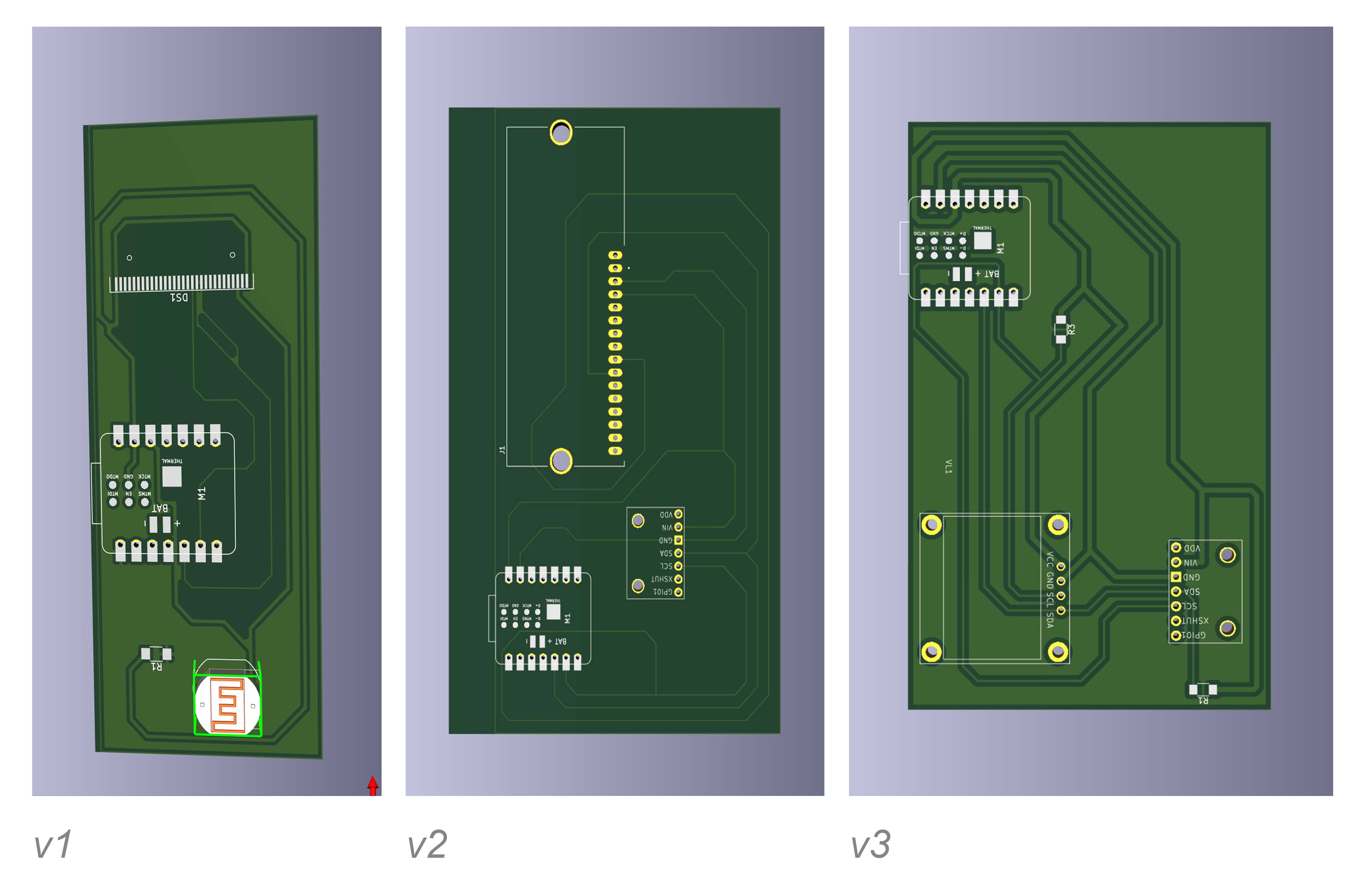
On a more pragmatic level. I learnt several things about using the program of KiCAD. Firstly, netlists are important. Netlists are representations of the connections between your components, and they can adapt according to where the components are placed in the layout. Naming your netlists allows you to easily adjust the thickness of your connections. You name your netlists in the schematic editor of KiCAD. When you are preparing to add copper fill zones be sure to select ‘’no net’’ so as to reveal all the routs between your components, and importantly press B to update or generate the fill. Through the course of this week, I went through 3 design iterations which each failed in some respects and worked in some other. I am hoping to use this knowledge to work towards my final project.

Iteration 1
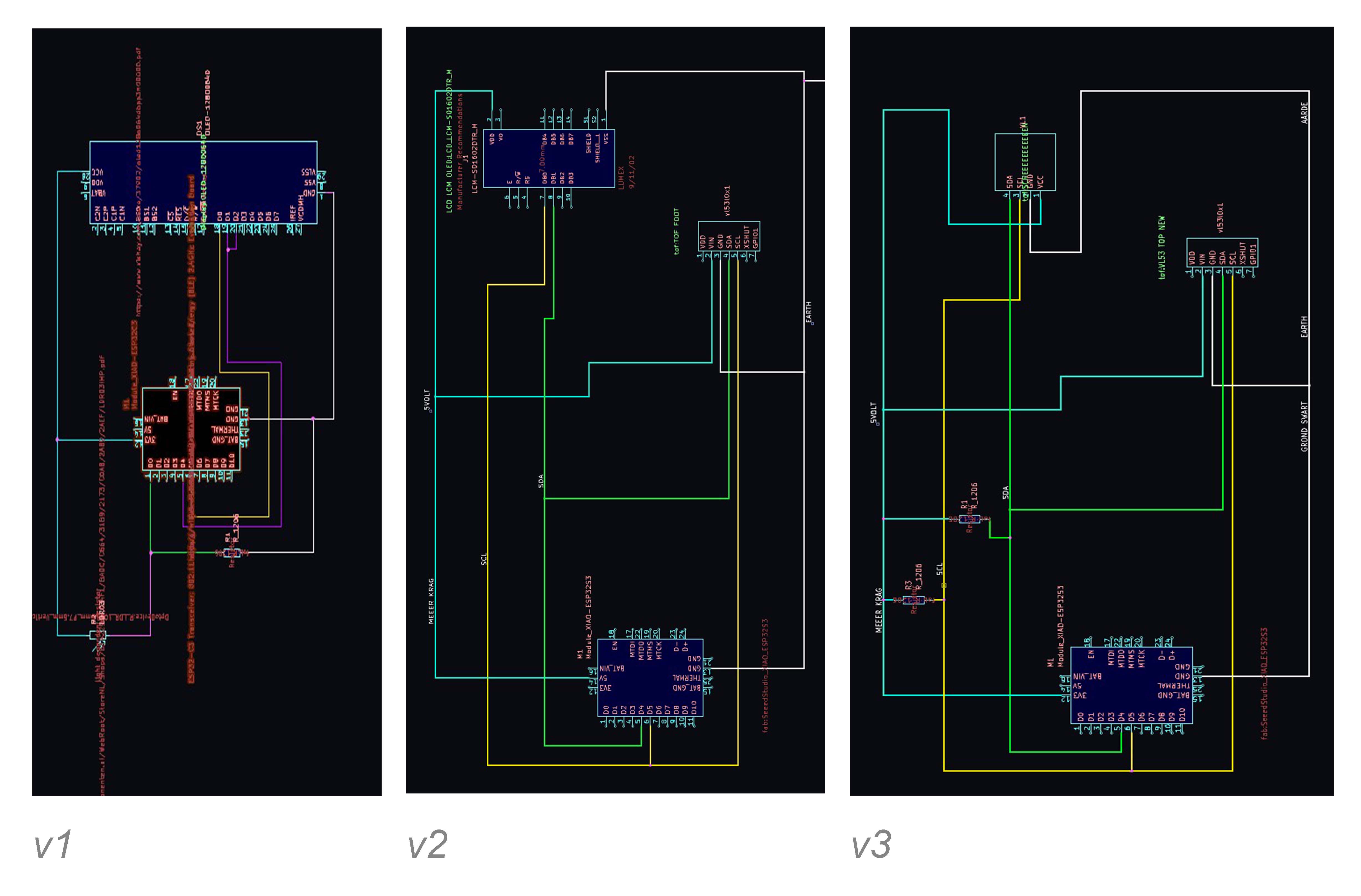
During my first design I struggled a lot with trying to figure out how to make my PCB boards work. Initially I designed a display which involved a light dependent resistor. I picked that design because it seemed the most complete and aligned with the trajectory of my final project, which is something which I try to do regardless of the iterations.
Iteration 2
I was quite surprised by the difference in scale of the schematic layout and the actual sizing of the components. My meeting with Anthony revealed that the wiring layout of the initial design had some problems as some of the cables ran in between the ports of the Xiao. I decided to try and find other solutions and started off by searching for the components which I wanted to use, and perhaps adapt the design somewhat.
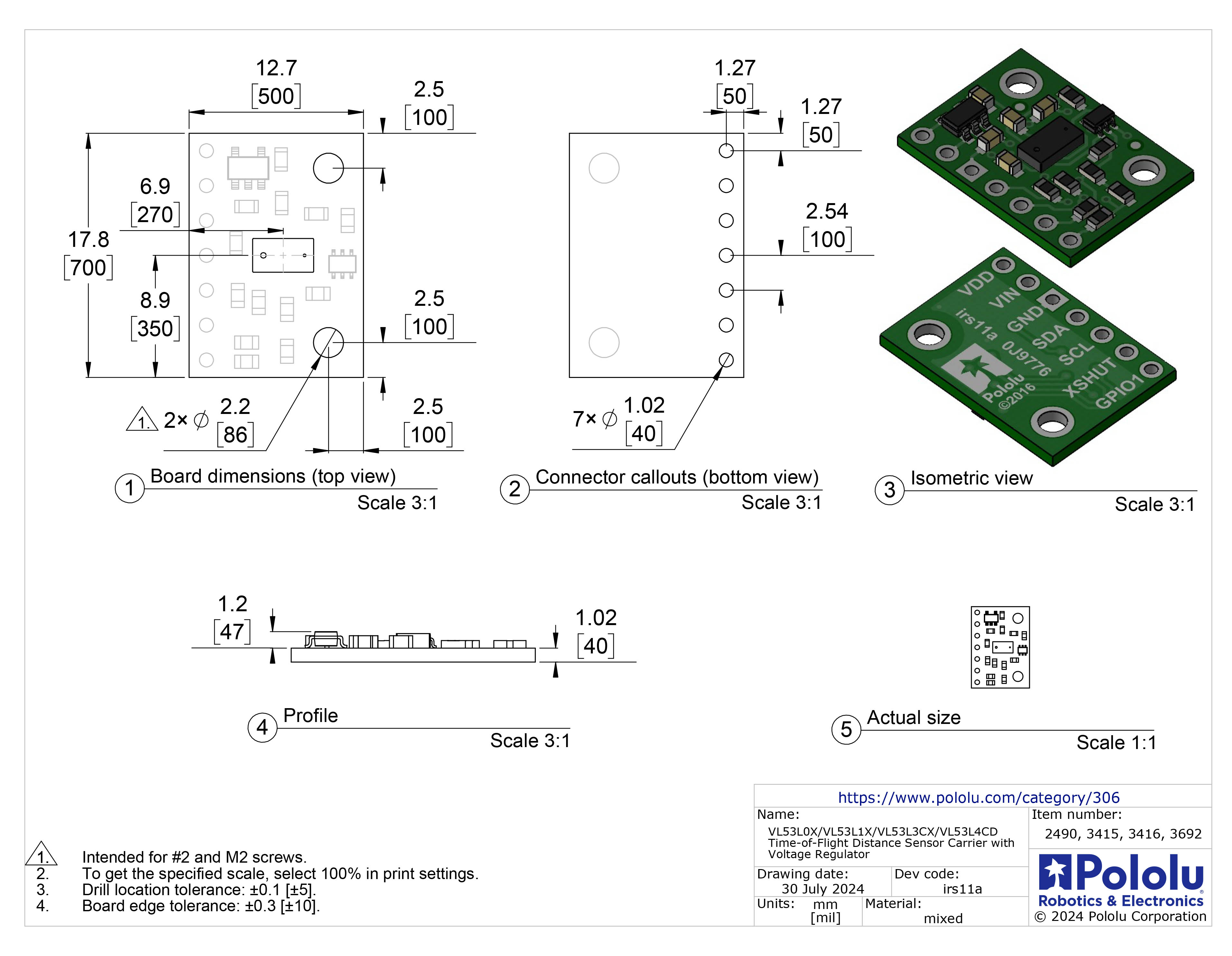
My meeting also revealed that there is a measure of interchangeability when using the same type of components, but different brands still require a look at the data sheet to find the corresponding ports. An example is that the ‘Time of Flight’ motion sensor does not label its VCC port as VCC, but rather as VIN.
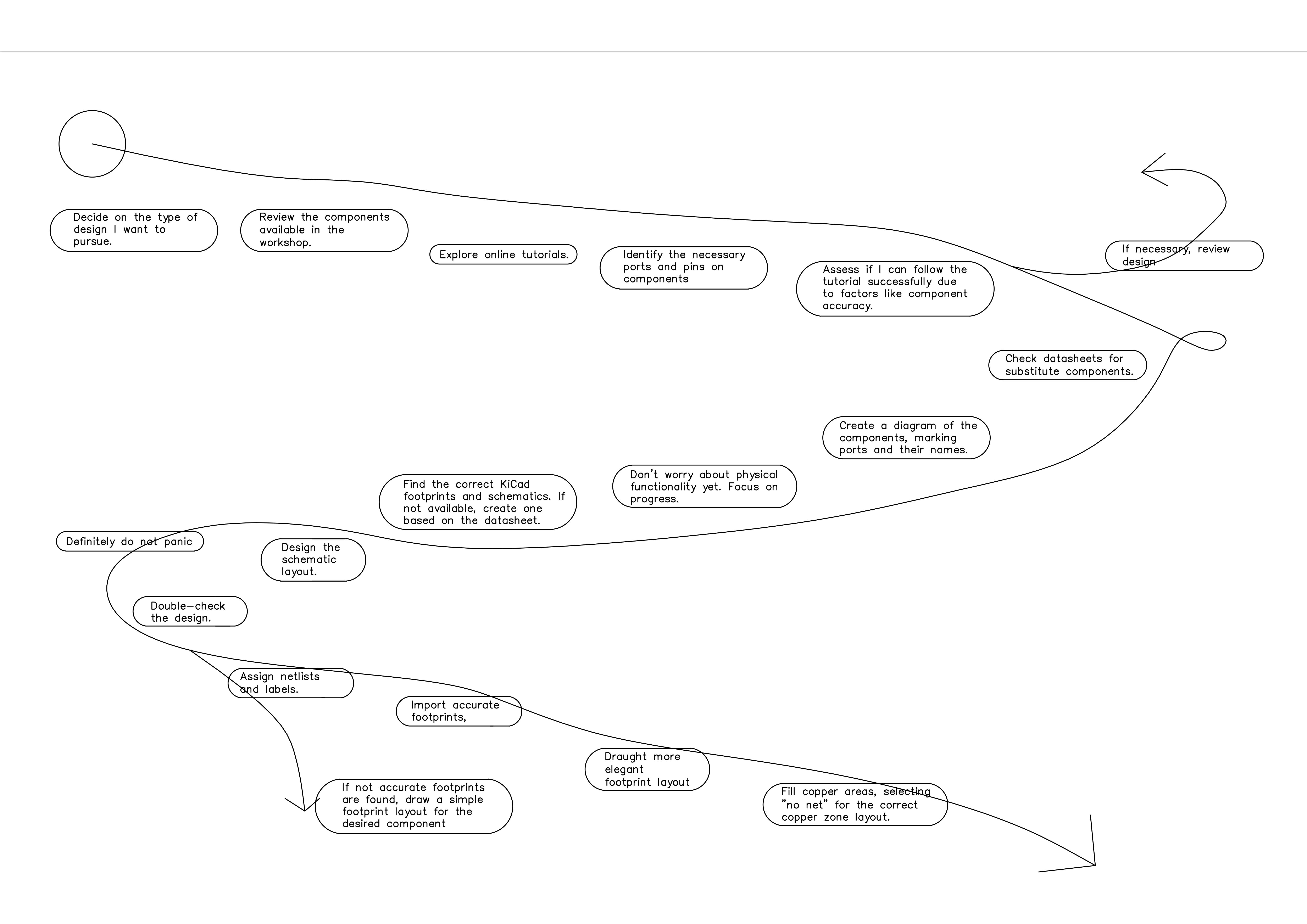
At this stage I had become quite overwhelmed with even 3 components. It is here where I decided to draw up a diagram which will from now on dictate my decision making with regards to electronic production/design. This diagram is definitely a working diagram and will inevitably change as I go.
When I returned to the design and tried to do a double check before I went to produce the pcb board I found that writing down your current understanding of pin connections and orientations in the form of an email helps with narrowing down the problem. This ensures that I understand the heart of the problem by trying to specifically describe and simplify my queries. I was mostly certain about my pin connections apart from the LCM and tried to find answers regarding this.
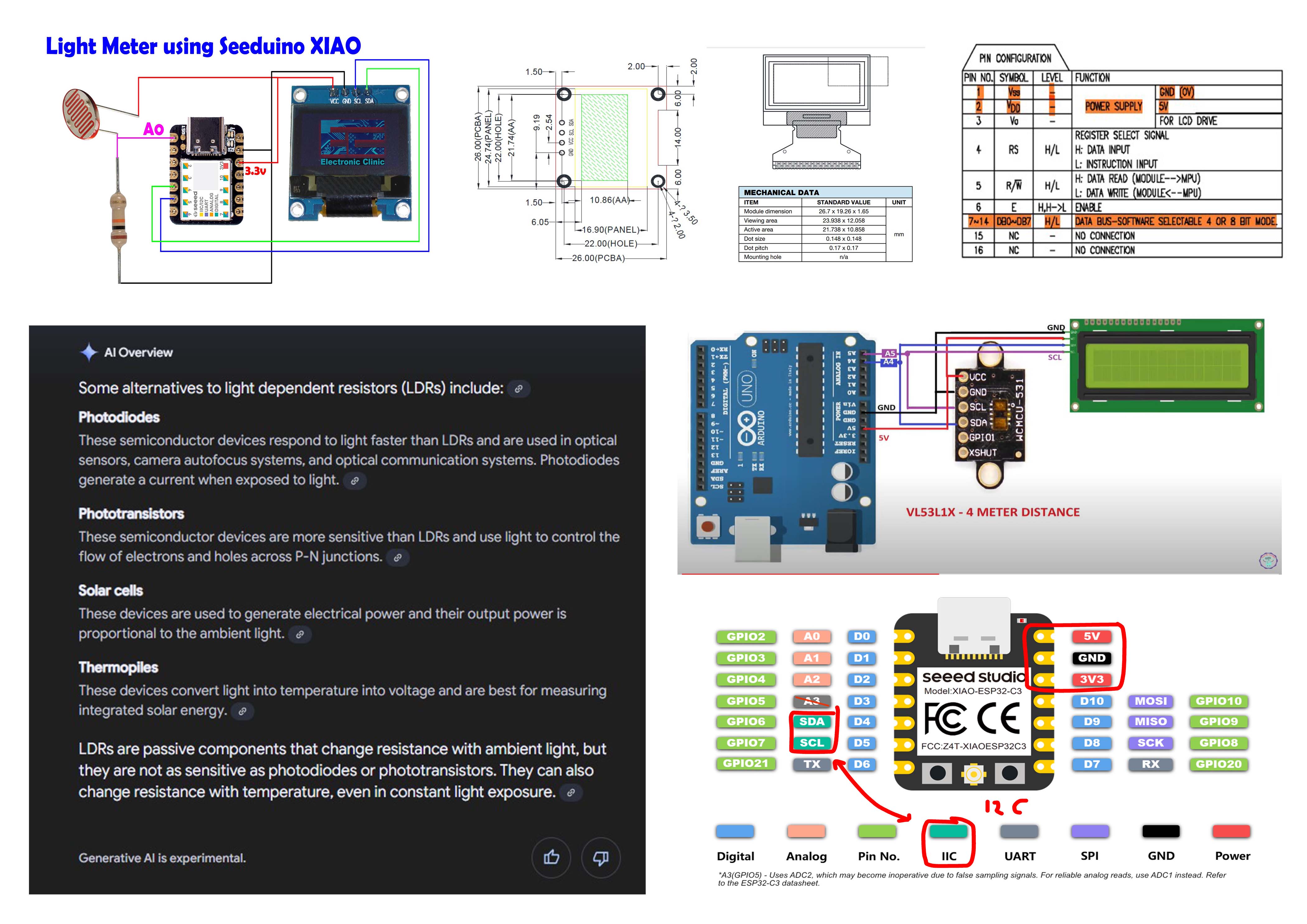
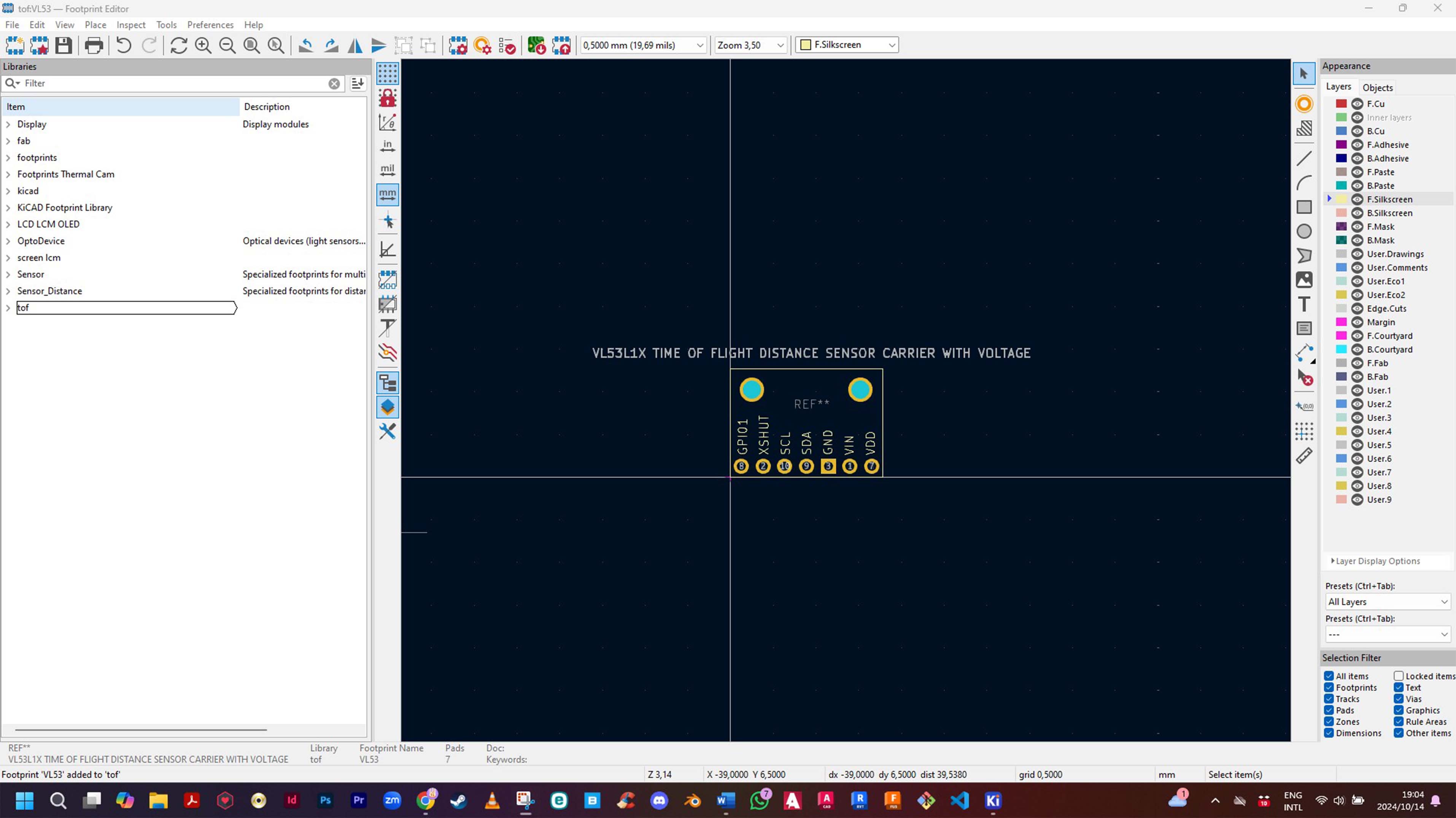
There are significant discrepancies between the components which you have in the workshop, the tutorials online, the footprints/ schematics in KICAD, and the simulation software like WOKWI. Trying to navigate this is perhaps the hardest part of this week.
Iteration 3
My short meeting with Anthony resulted in simplified components but a more intricate schematic design utilizing 2 resistors which link the SDA and SCL channels with the power supply. I struggled to navigate the steps all over again as I had to manually draw the component footprints for the screen. I also fixed layout and labeling issues which could have eventually caused a failure due to mixed-up circuitry.
Physical Production
When I started manufacturing the PCB boards, I started off by measuring the actual size of the components on KICAD. After that I found suitable copper surfaces. Due to the piece, I found I had to bandsaw the sheet in its width to ensure a length suitable for the actual size of the board. I decided to be conservative and estimated the board to be around 70mm wide. The sizing specified on KICAD was around 61mm.
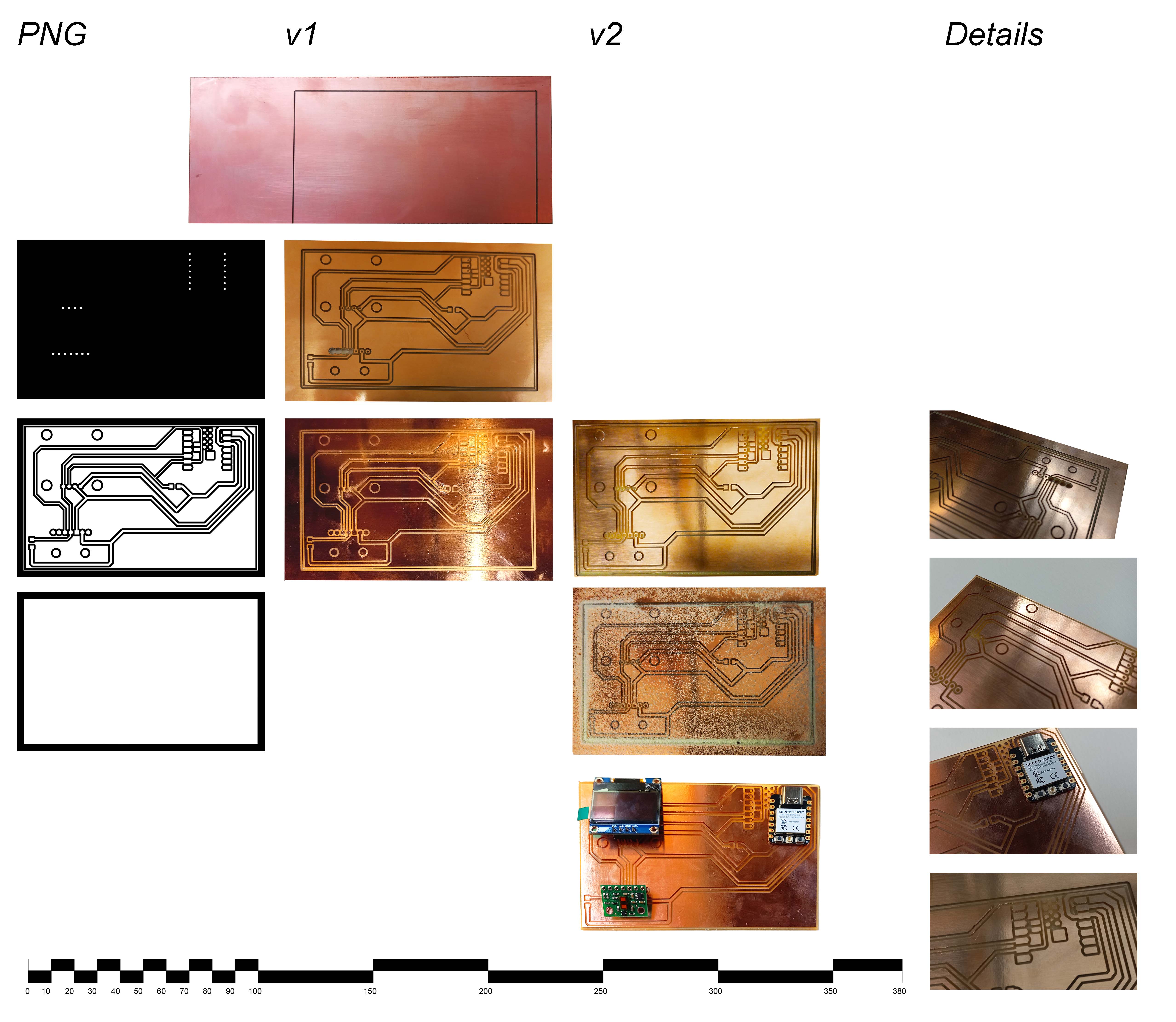
However, when I imported the Gerber images to the Mods app, the sizing was slightly bigger at around 69mm. I ended up trying anyway but the calibration of the machine was not the actual starting point of the routing and therefore the machine routed slightly over the edge of the copper, and I had to soon scrap that variation. I managed to find some other copper plates which were of a suitable size from the EECS lab.
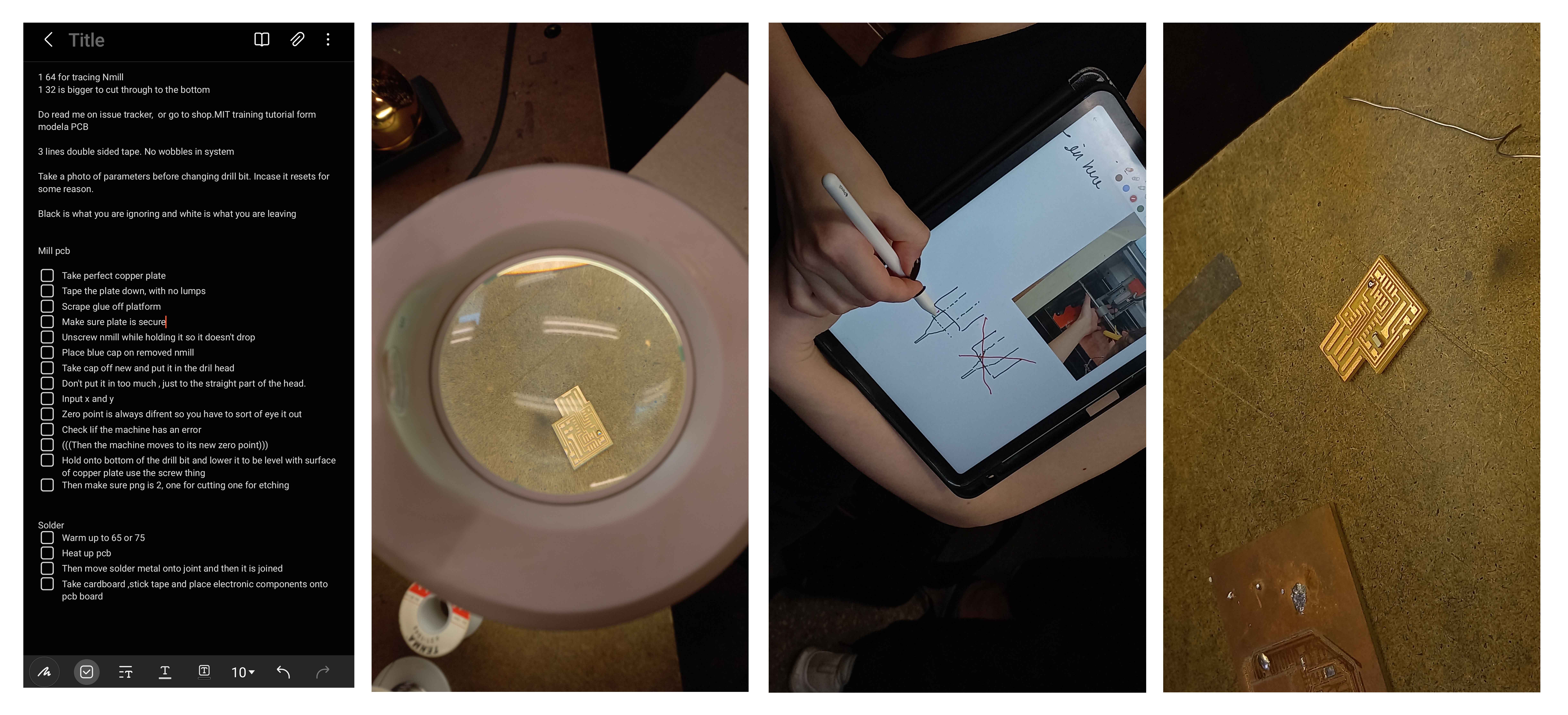
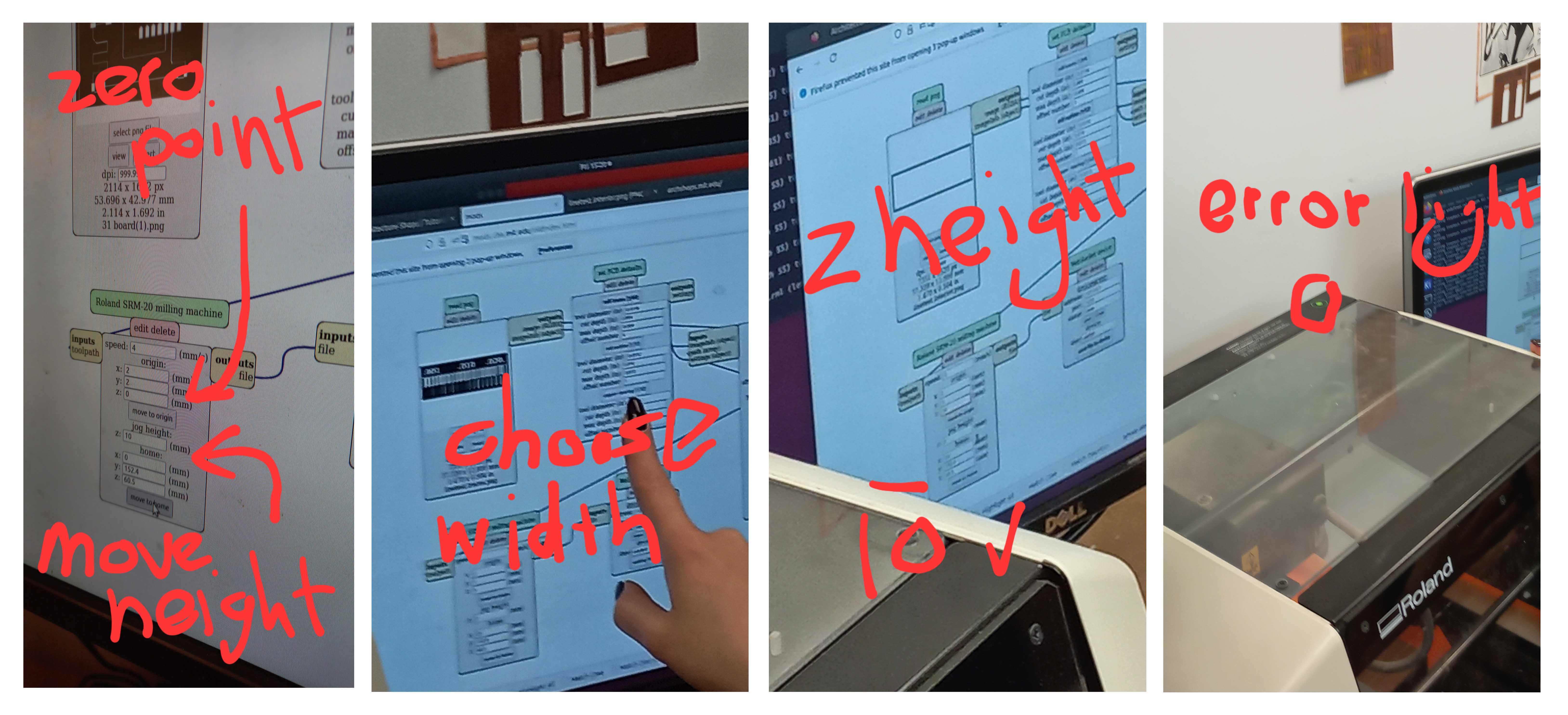
Step 1 of the routing exercise was successful as I applied loads of tape to the back of the board to ensure a secure stick. I also used the scraper to apply it even more firmly in place. I calibrated the machine and also noted that I needed to slightly force the mill-bit into the surface of the copper so that it doesn’t glide when it starts milling.
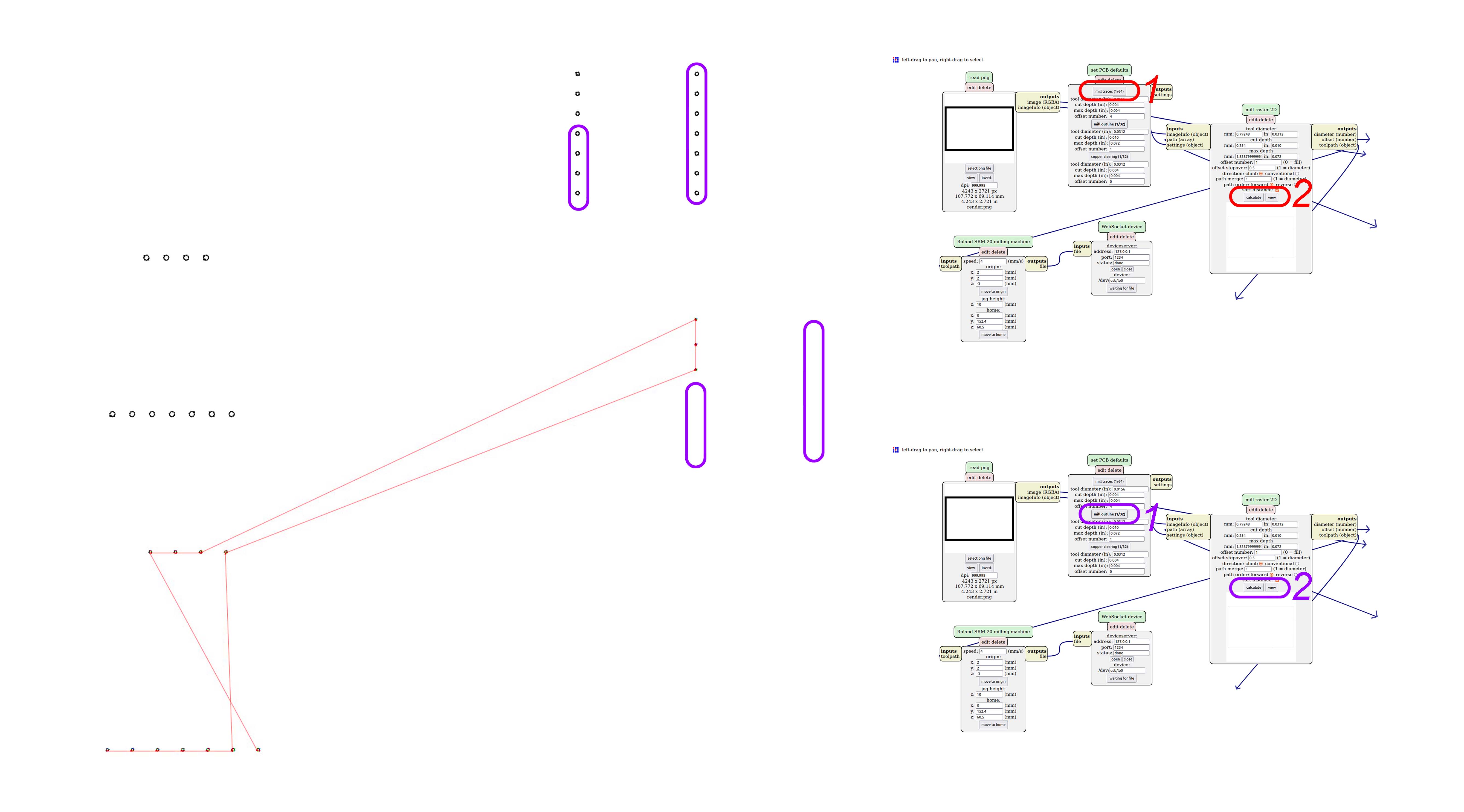
When I wanted to start cutting with the 32 n-mill the machine initially did not cut the holes to size due to the mods application assigning incorrect cutting routines. It cut 64 n-mill holes as full slices and I terminated the process after the 3rd hole was cut.
For some reason the milling paths were correct when I clicked on the 64 milling process and then calculated the final milling path, when I switched back to the 32 milling process and recalculated the same error I found on my first PCB reoccurred.
I gave it some time and after running through all the steps again on a second board I managed to drill some holes in crucial places, however the machine only drilled 3 full holes for the segment of the part required for the XIAO. I could live with this because the XIAO did not require holes necessarily.
After this step I started soldering the components. I did a test on the initial failed board by soldering two 10k ohm resistors to their respective positions and testing If they worked with the multimeter.
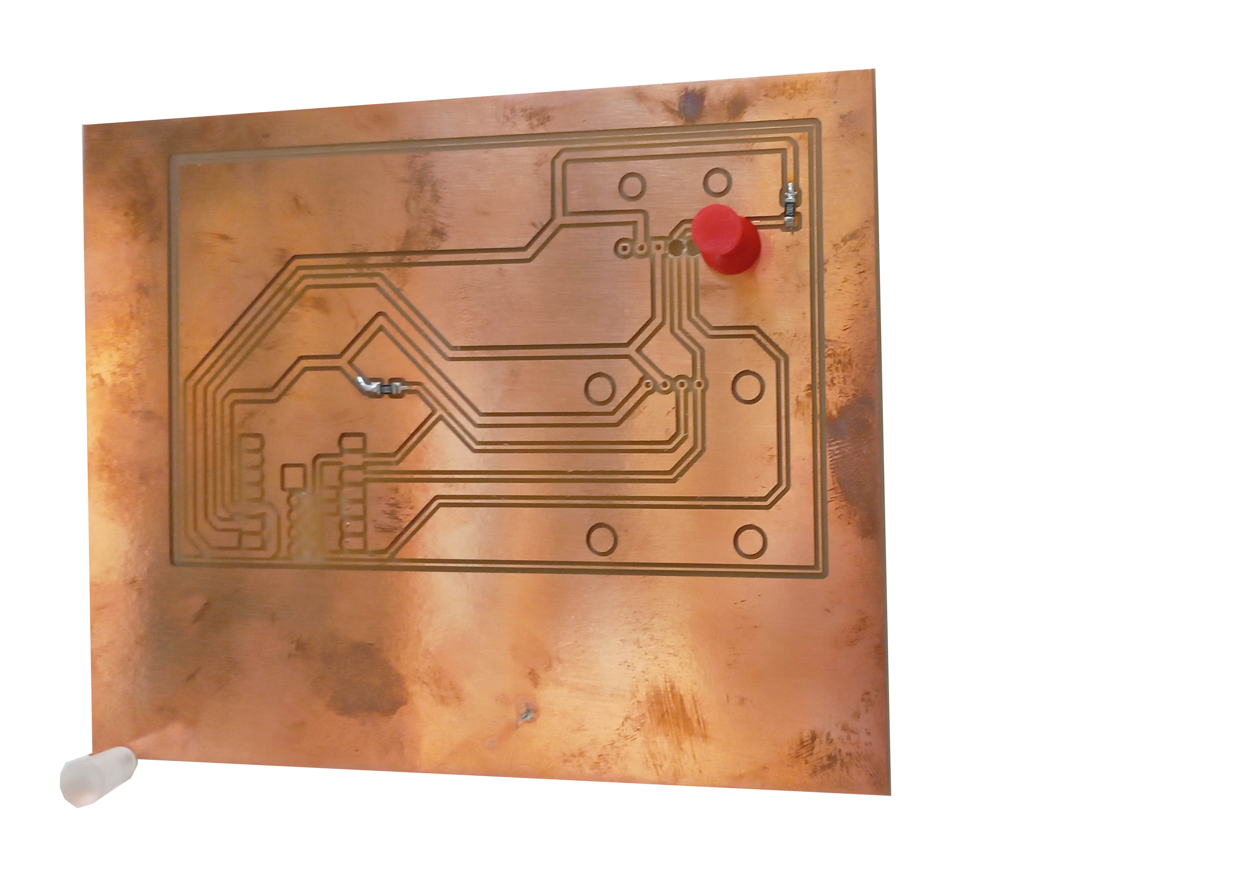
I was introduced to soldering wire, but didn’t use it correctly. Instead of heating the solder through the copper wire, I tried to dab at the excess solder with the wire. Which didn’t work. Reheating the already settled solder wasn’t ideal but I could manipulate the excess enough to guide it to the milled paths.
I managed to fix enough of the board to be confident enough to take it to Anthony at EECS without being embarrassed. He also helped me to use the copper wire correctly and to test the connections.
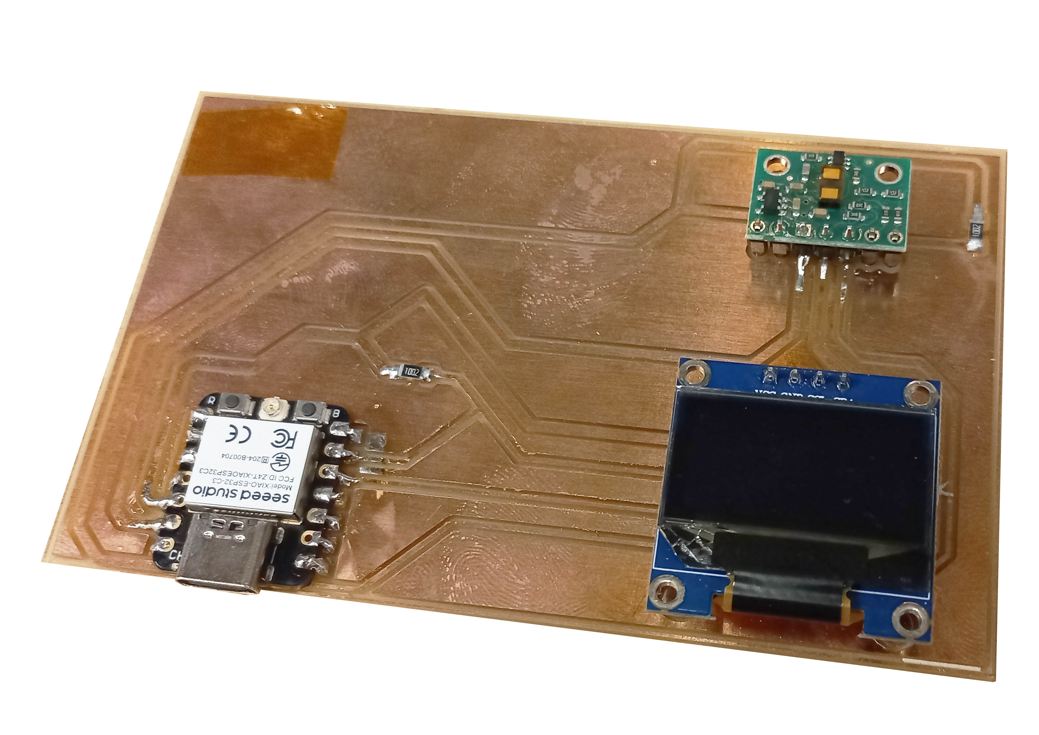
I applied capped-on-tape to the underside of the XIAO to ensure that there weren’t any accidental connections. Anthony gave me some excellent tips. 1-Always solder all the ports of the microcontroller for mechanical reasons and to ensure that you don’t accidentally forget one of the ports (especially if there are connections underneath the microcontroller). 2-You can add solder to the protruding pins if they move through the ports to simulate riveting (but its effectivity is questionable).
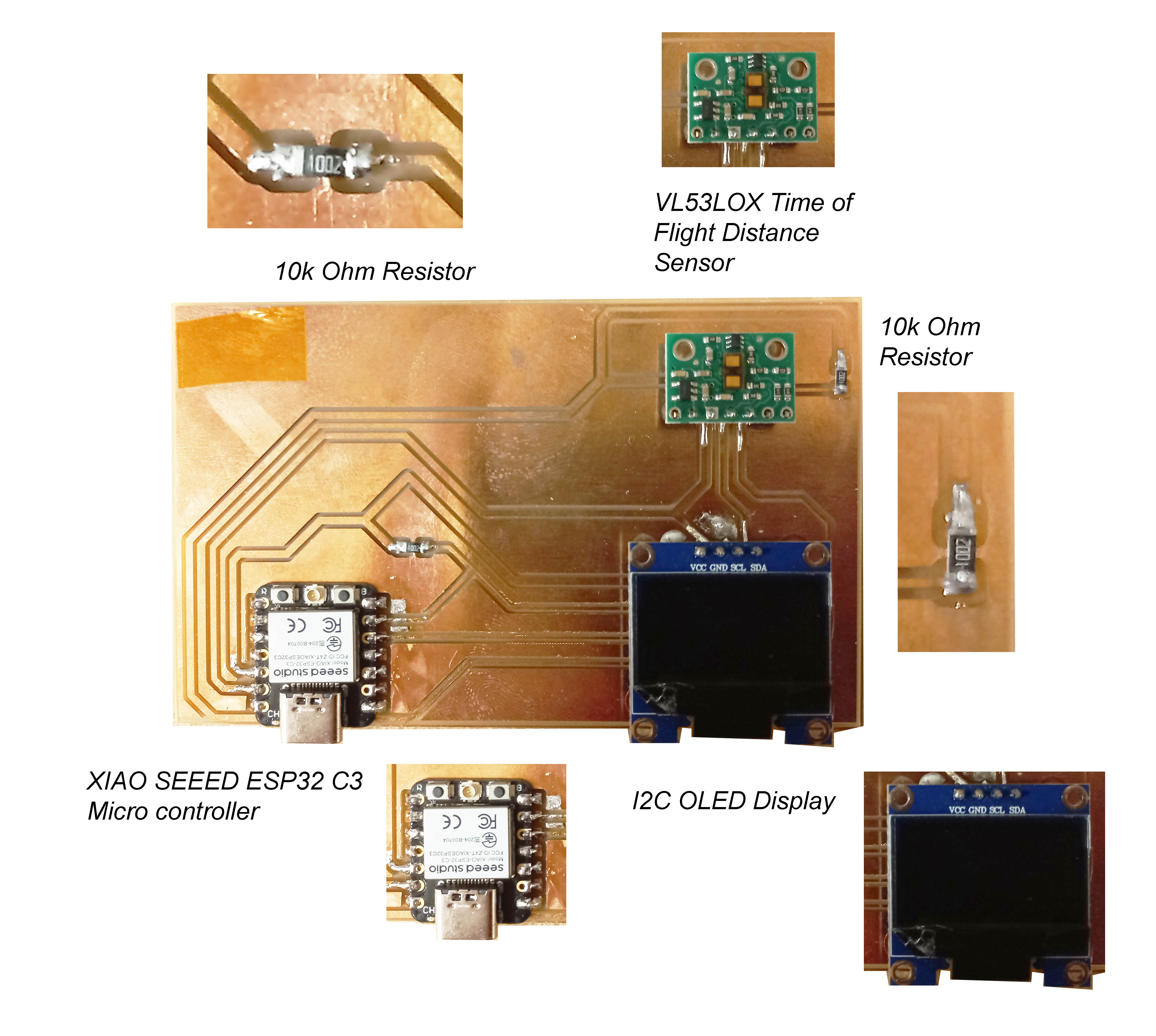
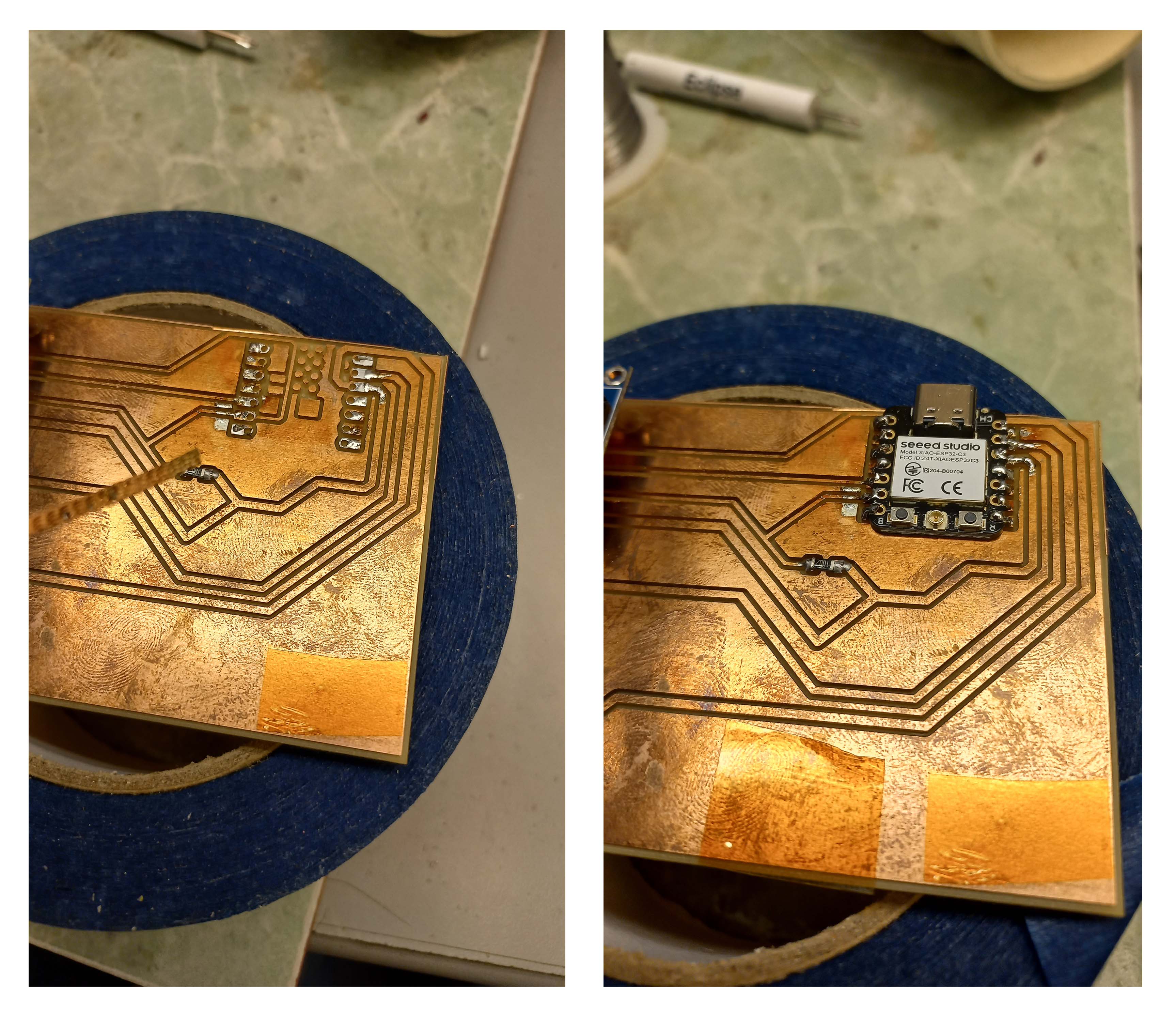
I found that double checking is quite necessary especially if you want to ensure that things go as smooth as possible the first time. Earlier this week when I tried to check if one of the N-Mills was sharp enough before milling. Shah suggested that I check underneath the microscope in the lab to see if the point has been broken or even sharp enough to do the milling correctly. the N-mill was broken but it gave me an idea to check my soldering under the microscope to see if I can notice any irregularities. Bellow is an image of the completed soldering before heading into software testing.
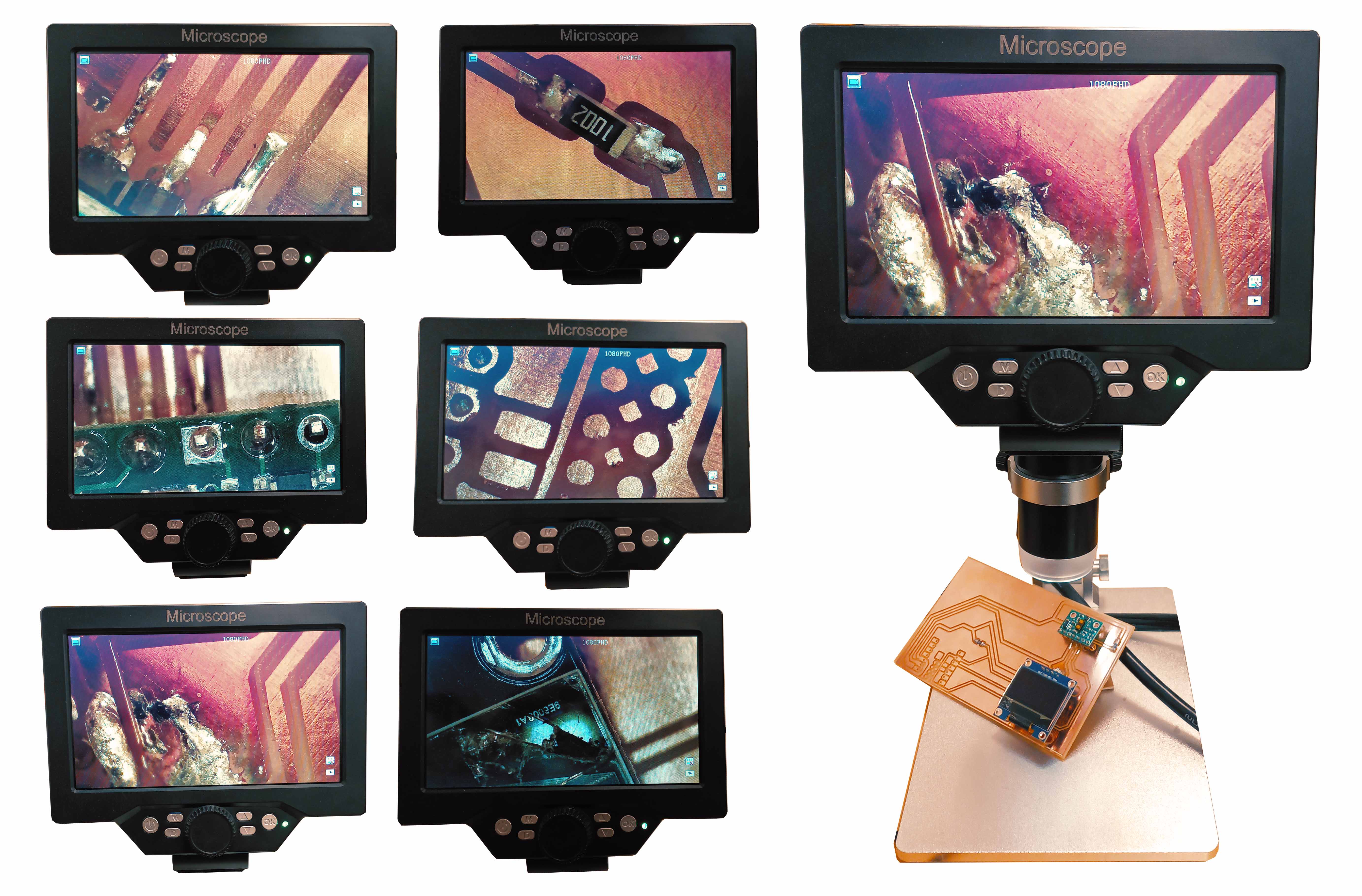
At this point I had finished connecting the hardware and it was onto testing the software.
Software testing
I started with some basic code which I found on a website which details steps to complete a Time-of-flight distance sensor and OLED screen configuration.
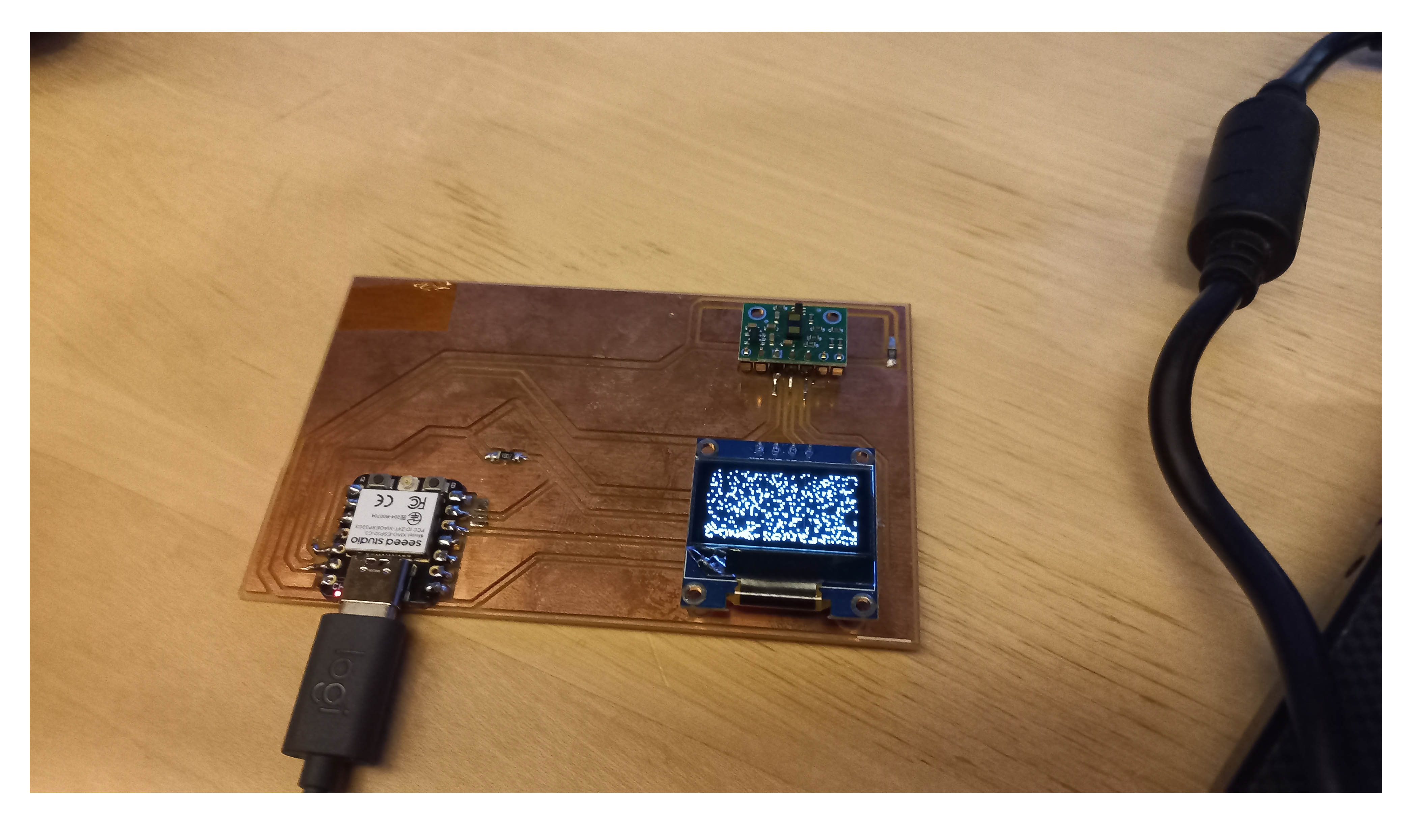
There were several obstacles which I had to navigate to reach a satisfiable conclusion.
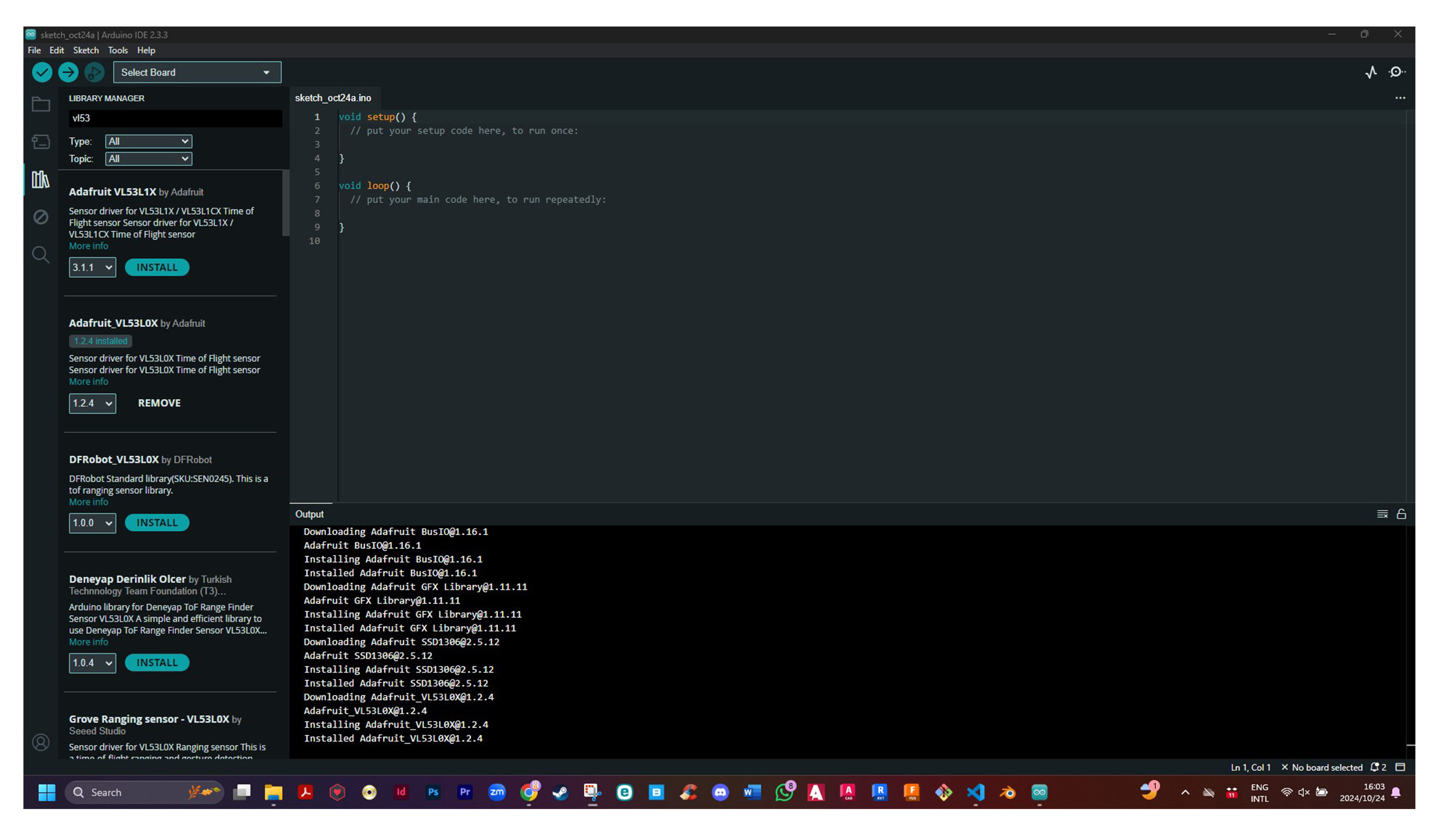
The first was to select the Xiao SEEED ESP32 C3 as opposed to the ESP32 C3 dev board from the list of boards available on the Arduino IDE platform. Once I did this (under the helpful supervision/assistance of/from Quinten) and removed the generic pin selection form the code, this caused the program to default assign the pins and the screen to light up. The screen, however, was not showing any new data and was showing some form of static.
The next day I went to speak to Anthony where I tried to configure the system to show the correct measurements i.e. the distance to the object in front of the sensor in millimeters.
Coming from Quentin, we understood that the issue was a coding one since both ports were being identified by the test signal being sent out by the XIAO. Before we started adjusting the current code, we ran tests on both the OLED screen and the VL53L0X. The screen completed its test, but we had some trouble with the VL53L0X, which failed to boot. Anthony delineated the problem down to the fact that I wasn’t using the correct library and that in fact my physical component was the VL53L1X not the VL53L0X.
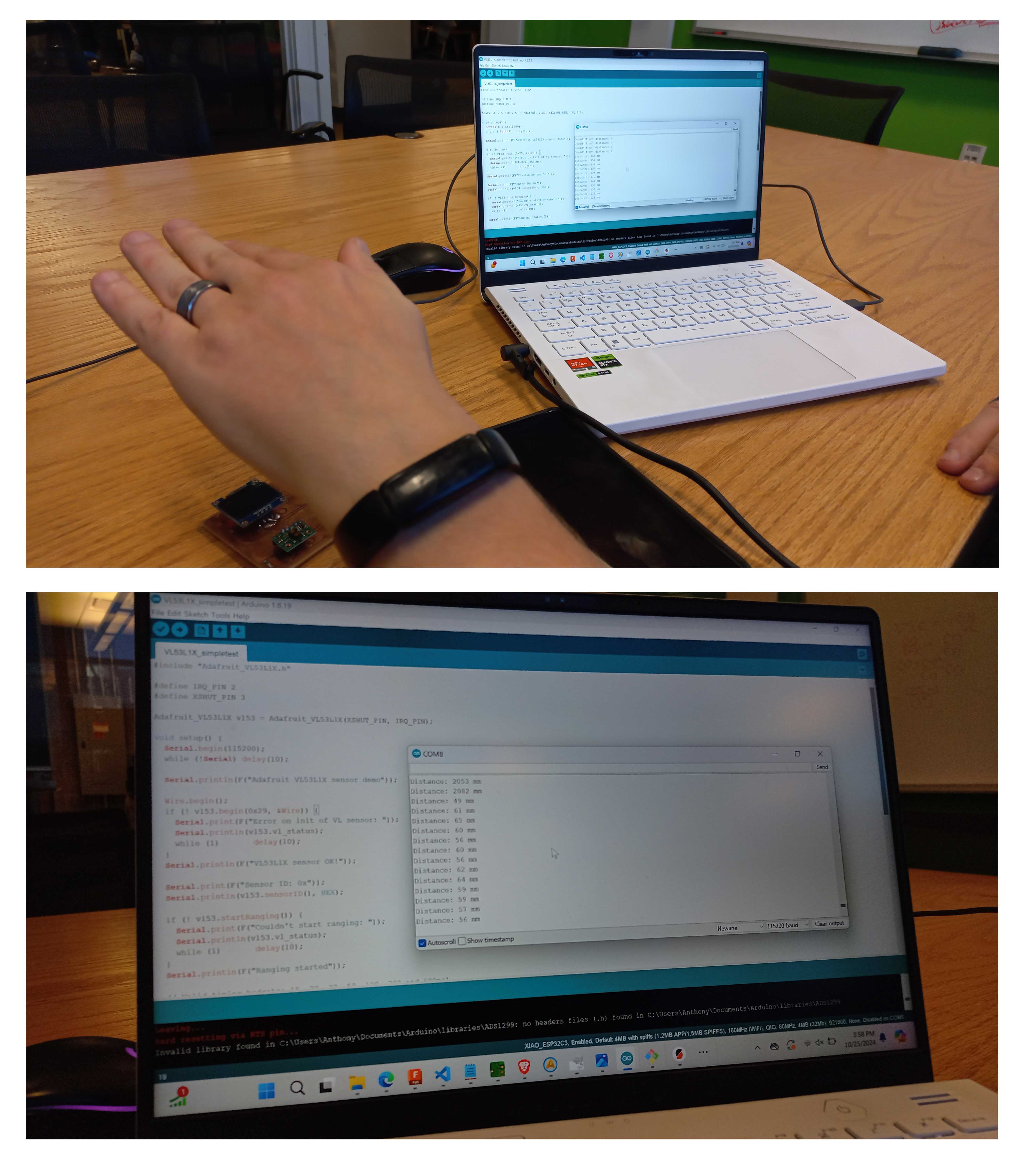
Once I reinstalled the new libraries the VL53L1X was showing the correct measurements on the serial monitor. At this stage Anthony identified that the problem was one with the Xiao itself because when we fixed the code and uploaded it to hardware, it did not want to run. The only solution for moving forward was going to be to replace the Xiao with another identical Xiao.
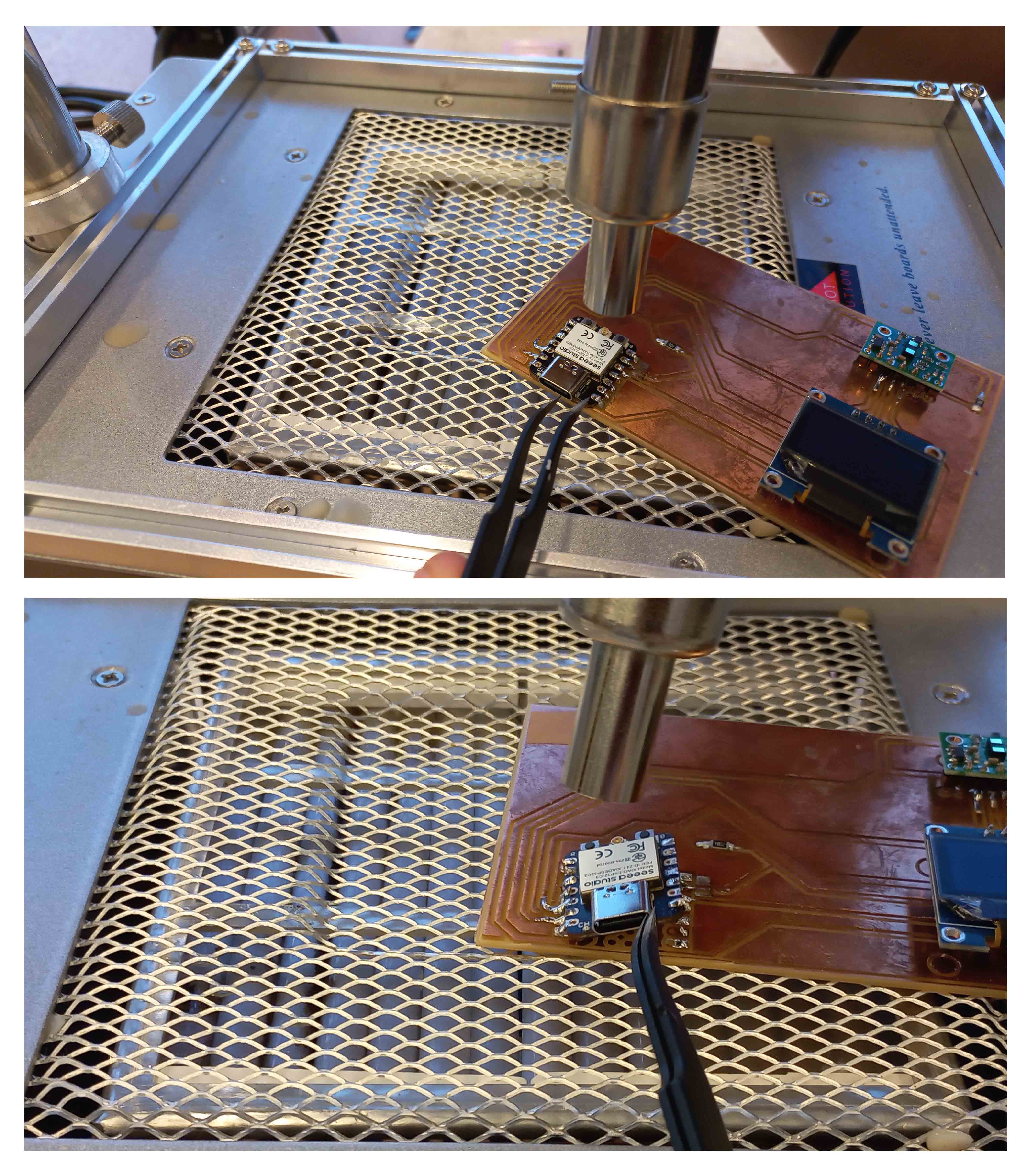
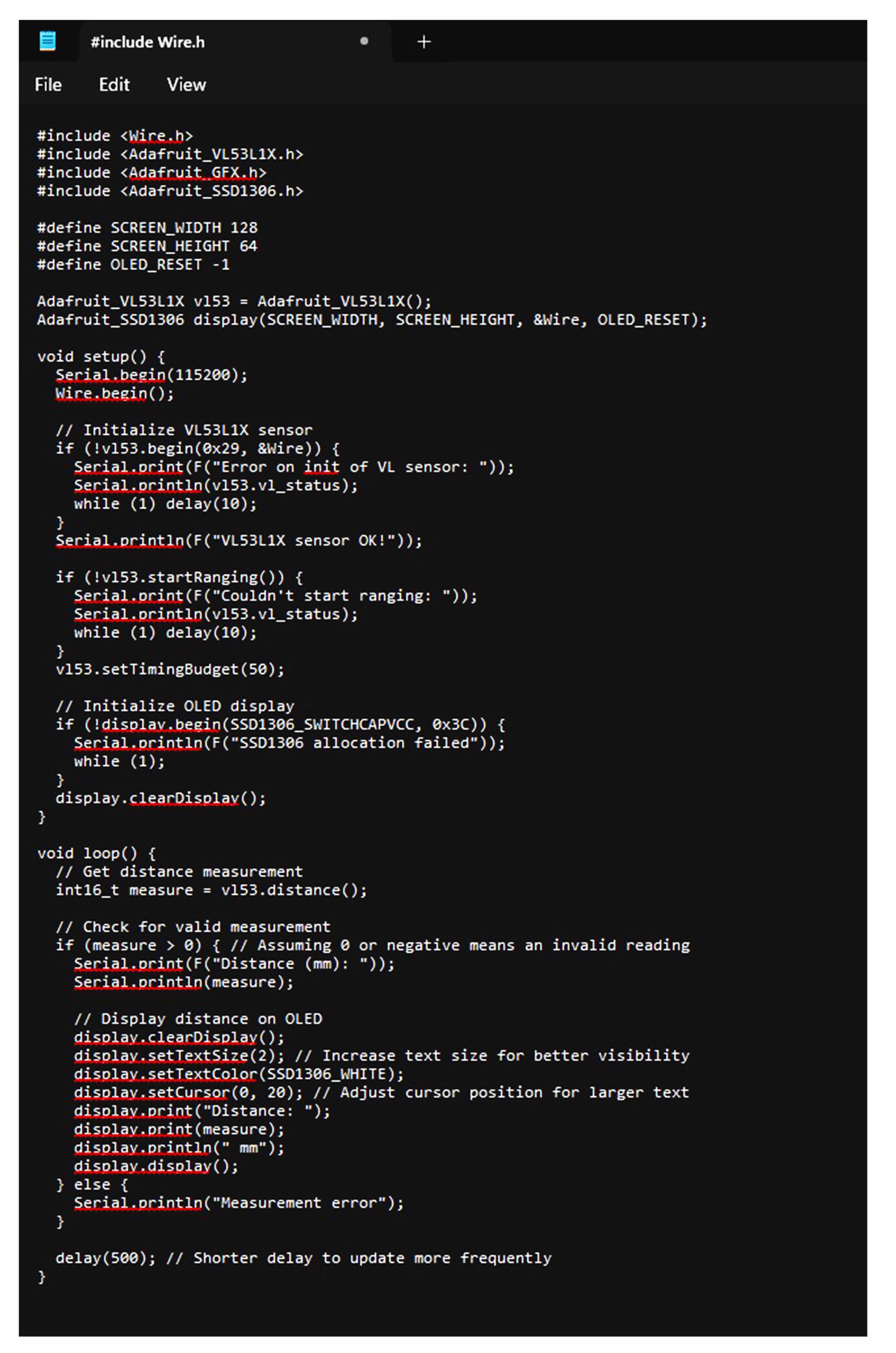
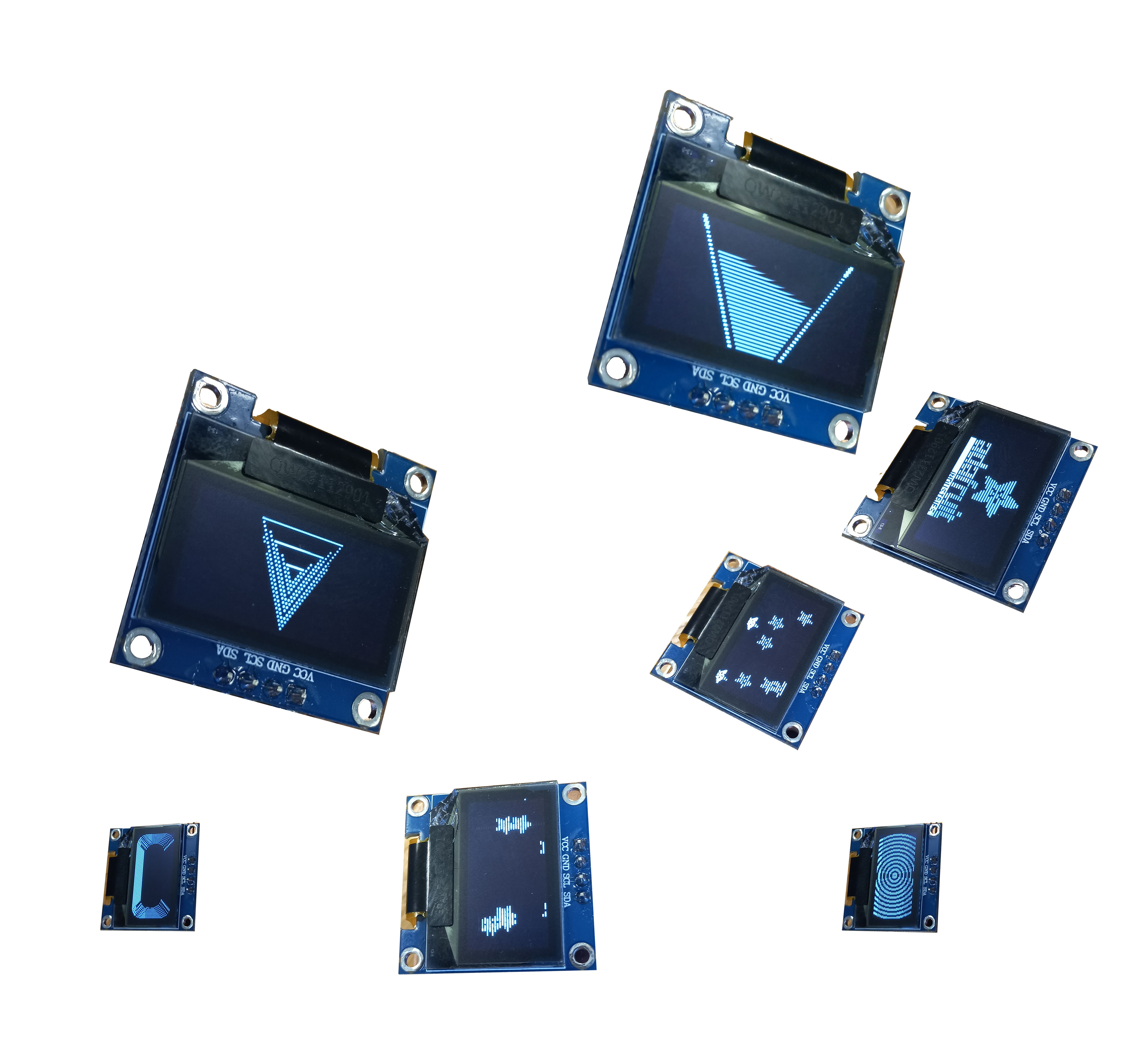
After Anthony showed me how to do this using the hot air station, I resoldered, cleaned up and re-taped my new Xiao. I went to install the components, and it seemed that the screen was showing digital braille. I went to back to the code and discovered that there were some problems – there were redundant lines in the code “setup” section. I added a validation check and quickened the display timing to 250ms.
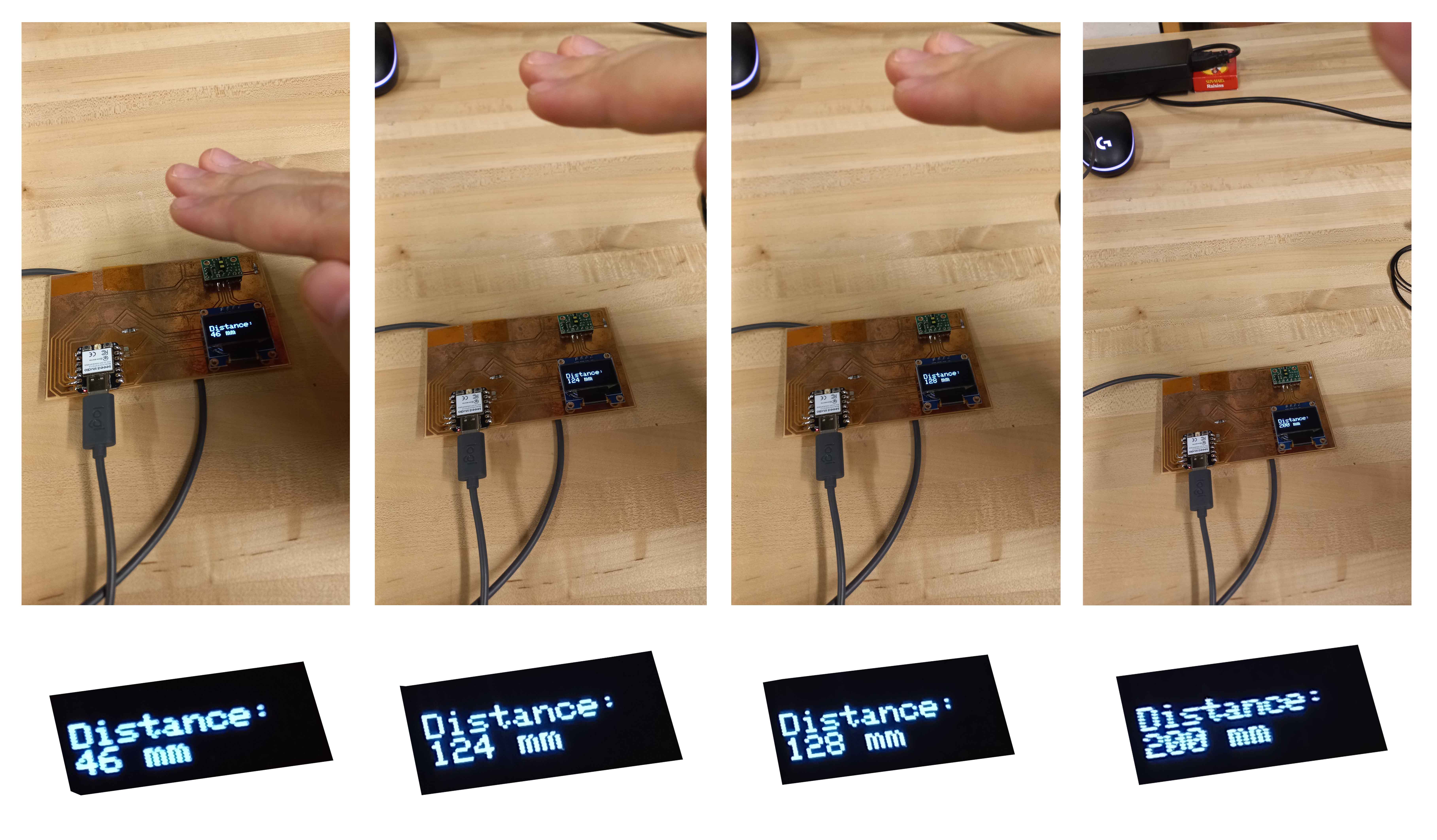
The result seemed to be that the braille was now moving, and it looked like it was showing the measurement. I noticed that the pixels corresponded in size when I moved my hand closer and farther away. This suggested a sizing issue and after I increased the text size it worked.
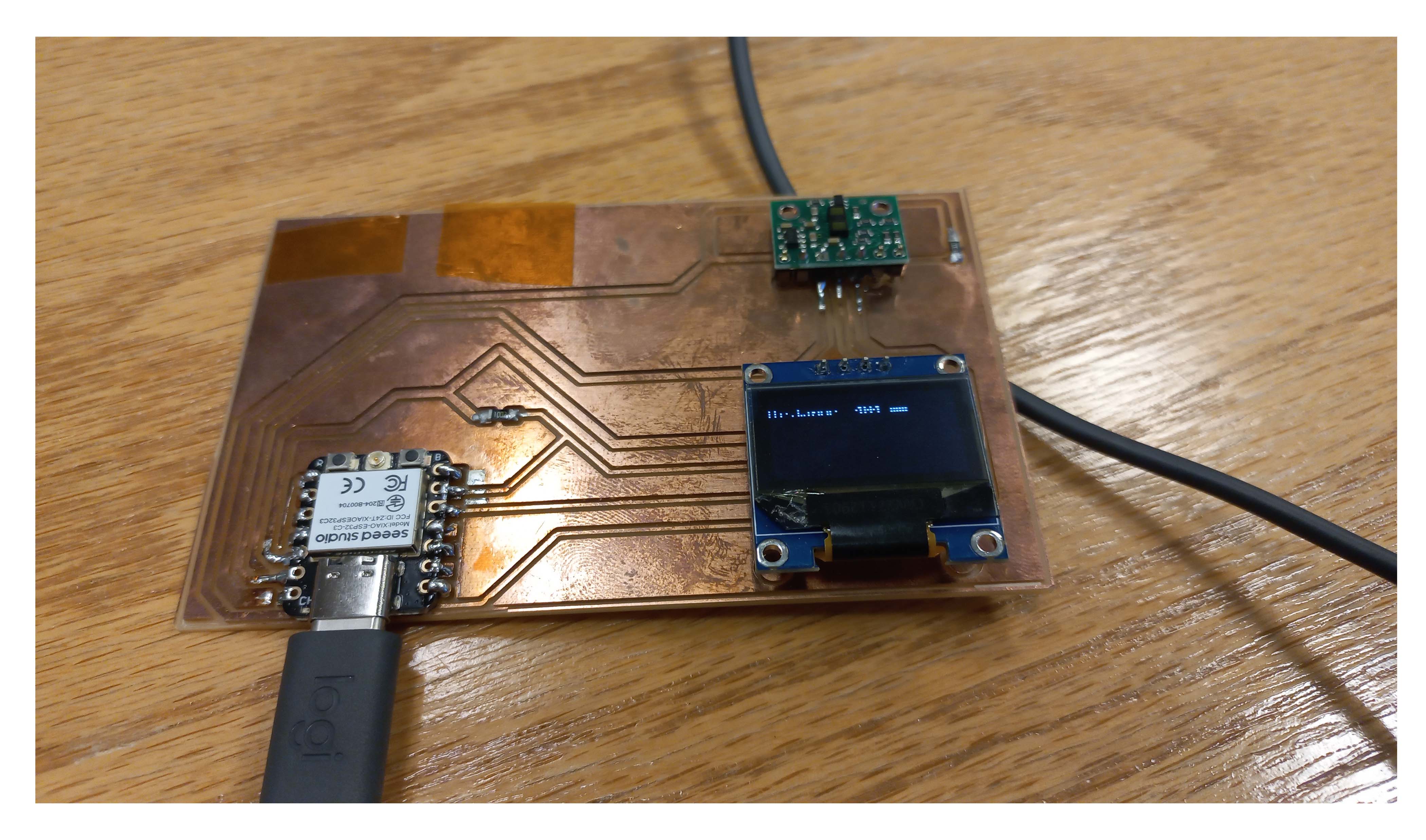
I was so happy!
