Electronics production
This week we made an in-circuit programmer by milling the PCB, and programming it. I followed Brian's tutorial for the whole process.
PCB milling
For the PCB fabrication, I downloaded the class PNG files for both the traces and the board outline. I used the Roland SRM-20 milling machine with the default settings:
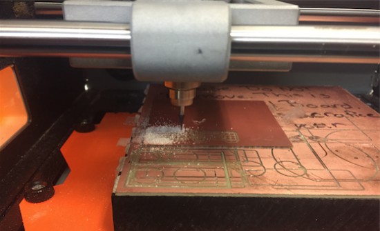
Roland SMR-20.
And here it is the result:
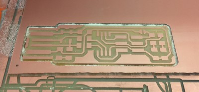
My first PCB ever
The cut was pretty clean, I just had to remove a tiny bit of copper left at the edge of the board (next to the USB pads). I used a knife for that. Then, I clean the board using GOJO, and it was ready to be stuffed!
Assembling the PCB
After gathering all the components, I followed Jackie's advice and place them on top of a printed copy of the circuit diagram. Even though I was trying to be careful with the polarity of the zener diodes, LEDs, and the ATtiny45, I messed up with one of the diodes (and only realized after I finished the soldering!).
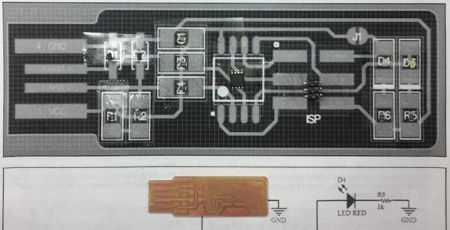
Board components on top of the circuit diagram
I placed the components as followed:
I had soldered in the past, but this was my first PCB stuffing. I used double-side tape to fix the PBC to a piece of cardboard to facilitate the process. We were also recommended to put a tiny bit of solder of the board for the first connection of each component. Then, place the component on the board and solder that pin. Finally, solder the rest of the connections of the component.
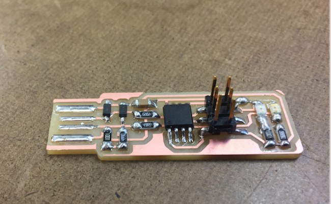
After finishing the stuffing, I used solder to create a bridge on the J1 jumper. Last step was to flow some solder onto the USB pads to improve the USB connector. I had to do this a couple of times until my board fit tight into the USB port. And voilà!
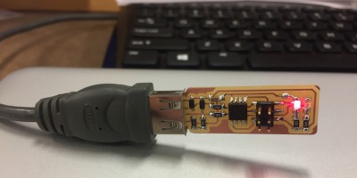
I got red light! This may work...
Programming the new programmer
For this part, I used an AtmelICE device (programmer) to program my board. Brian's tutorial describes the entire process quite well. I (1) downloaded the last version of the firmware, (2) built the .hex file to get programmed onto the ATtiny45, (3) updated the Makefile for the current programmer [i.e. 'PROGRAMER? = atmel_ICE'], and (4) erase the chip and program its fash memory with the .hex file.
Then (after I checked the USB functionality), I blowed the reset fuse and removed the bridge on the J1 jumper. Finally, I goy my very first working ISP programmer!
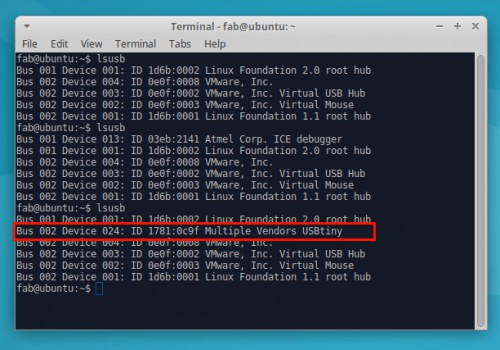
..and Linux recognized it!
Next steps...
I didn't have time this week, but I'm planing to play with other PCB processes. I'd like to try the vinylcutter and see what I can do...
Files