Week 5: Electronic design
Week Summary:
I drew the schematic and PCD layout of the Hellowworld PCB, milled it, populated it with components, and programmed it with my USPtiny programmer..jpg)
ASSIGNMENT: Redraw Neil's Echo Hello World board w/ your drawing tool of choice and add your extra parts/designs. Make the board and test it. The group project is to use the oscilloscope and volt-meter and be comfortable w/ electronic test equipment.Circuit Design:
We are given the schematics below and tasked with redrawing the board and adding components. Here is the given board layout: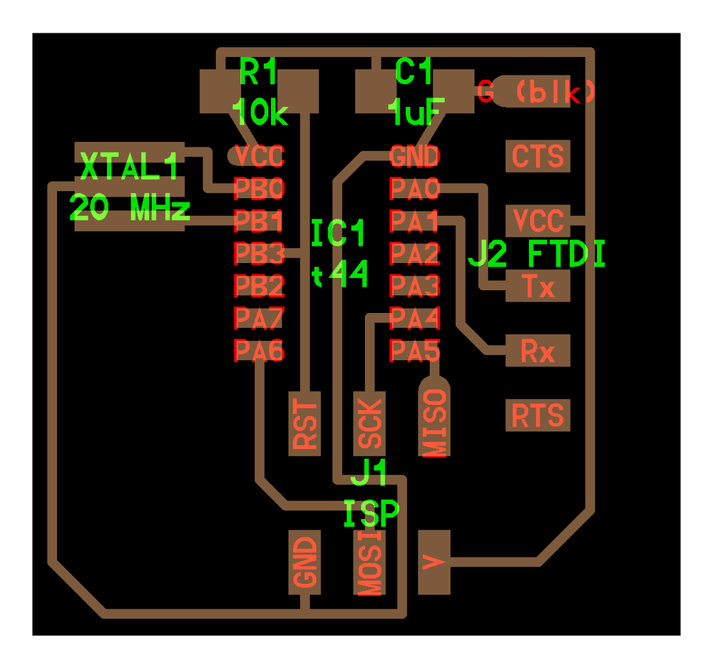
List of Components: (1) Attiny44-SSU (the microcontroller) (2) Crystal Resonator (this create precsise oscillations, it's a better timer than the one that comes on the Attiny) (3) 10k Resistor (A pull up resistor for the reset pin) (4) 1uF Capacitor (bypass between power and ground) (5) UART Pins that allow communication between the microconroller and a PC via USB. These connect to a cable like this one:
Simplified diagram of how serial signals are transmitted and recieved:
(6) ISP header This is how you connect the programmer to program the board. In week 3 I made an ISP programmer that I'll be able to use to program this board. Before adding my own designs I drew up the original Hello World board. I began designing my circuit & PCB using KiCad. I followed the guidelines on the Class Site. To get all of the needed footprints of the circuit components I uploaded the class kicad library to my KiCad.
After uploading the library of fotprints I opted to watch some helpful tutorials about KiCad that taught me helpful shortcuts. If you hover your mouse over a component: M=move, R=rotate, V=value, Delete=delete. To select a new component press A to bring up the menu. I populated the schematic with all the components for the HelloWorld board. Here is a look at that process:
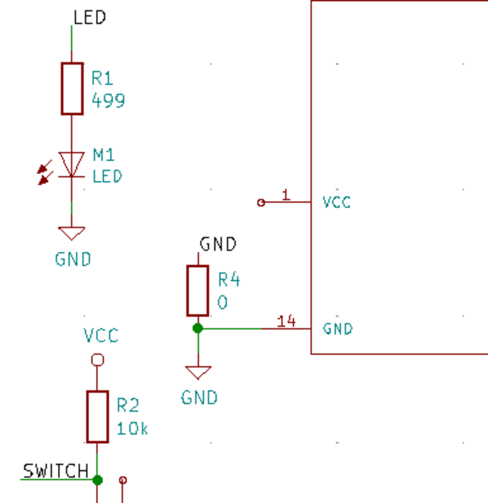
I labeled each node and used that to connect the ports of interest.
This made adding the UART and 2x3 header prety simple, all I had to do was label them too! The Hello World schematic:
NEXT, I added "my own" components: (7) LED & 499 Ohm resistor to pin 6 (8) Switch from pin 11 to ground w/ a 10k Ohm resistor to power I opted to not go creative on my additions. Final Schematic:
Next I had to create the PCB. Before being able to do this I first had to match each of my parts to a footprint, this was tricky to figure out at first but I found that the process for that is: (1) Click the assign PCB footprints button on the top menu (2) Click on the component you want you assign in the middle panel, then scroll through the left panel for the type of part you want (3) When you find the type of part a list of them will show in the right panel, double click on you one you want to assign as the footprint and that's it! Pic of footprint assigning:
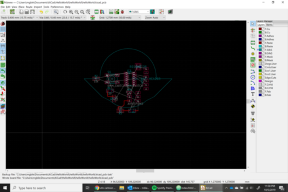
To create a PCB from the schematic you follow this process: (1) Click "Generate Netlist" in the top menu & click it again in the panel that pops up (2) Save the netlist as a .net file with your project (3) Go back to home and click PCB Layout Editor (4) Click "Load Netlist" in the top menu of the PCB Editor (5) Click on the schematic and your parts all appear in a rat-nest Here are all my components before I put down any traces:
Next I went to File -> Board Setup and changed my clearnances, trace widths, etc, to match what would work with the 1/64" end mill of the Roland mill in the Archlab!
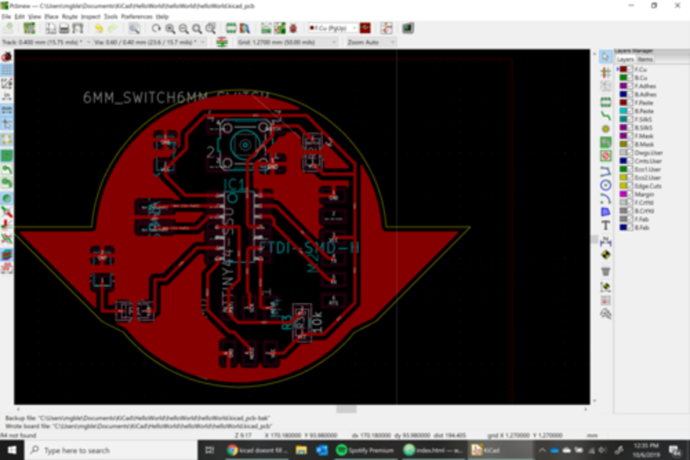
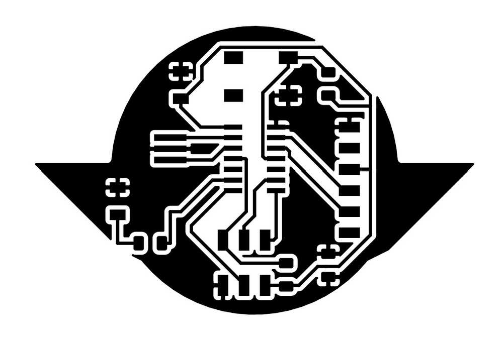
Next I rearranged my components and iterated through trace connections until I got a configuration that worked. Half way through I decided to make my PCB look like a UFO since my final project will be a UFO (BUT in reflection it definitely looks more like Yoda). I think in my final project I'll have a clear compartment where you can see the cool PCBS :)
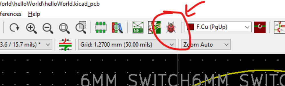
I finally wired all the traces, but the final issue was that the GND filled-area, a portion of the board was unreachable, meaning GND couldn't connect everywhere it was needed. I found this out via the Design Rules Check button (which looks like a lady bug!). This is a super handy tool that tells you what things aren't connected, or where some traces are too close. To get around the error I was having I added a zero-resistor to jump over one of the traces.
Adding zero resistor:
Final PCB layout
Here is my final PCB layout and the .SVG files that show its traces and outline:
Next I milled the board with the Roland Mill in the fab lab. My first issue was that I accidently drew my board edges in the wrong layer. This ended up giving me trouble when trying to upload the above .svg file to make my edge cuts. The line was so thin that the mod only idetified some of the edges to cut and wouldn't have completely cut it out. When I realized my issue I went back into KiCad and made my edges into the edge cut layer:
.jpg)
After fixing this, tragedy struck when the end mill decided to cut directly into the middle of my PCB right as it finished making a beautiful cut following an equally beatiful traces cut.
.jpg)
I redid the traces and edge cut and this time the mill didn't eat it.
Next I got all of my components from the lab storage and start soldering them all on.
Finished Board:
I used the arduino software to program my board and used Jaclyn Berry's page as a reference. I used her blicking code example as a jumping off point. My first lesson was in making sure that all of your Arduino board and programmer settings under the tool menu are right. For this set up my settings under the tool menu were: Board: "ATtiny 24/44/84" Processor: "ATtiny44" Programmer: "Atmel-ICE AVR" My next lesson was in the naming of the Attiny pins. This diagram shows what the pins are named in the eyes of Arduino vs. what you see on the schematic.
My LED pin is A7 and my switch pin is A2. This took a sec to figure out. My final test code was this (.ino file linked here):
It successfully uploaded and the button could turn on & off the LED!
Next I made a connector cable for my PCB and my programmer from week 3 .
Once I had them connected all I had to change on the computer was the Progammer option under the tools menu. For my set up the correct info is:
I uploaded the same code to this programmer and it successfully ran on my PCB!
-------------------------------------------------------------------------------------------------------------------------- NOTES FROM 10/2/19 CLASS: Information about PARTS ------------------------------------------------ This week are are assigned to start w/ Neil's hello world board and add components that we want- at least adding a button and an led and making them do something. (Next week we're programming our board.) We have access to the fab lab inventory, digikey section shows the components we have in our lab. Capacitors are most commonly used as filters, on the hello world board. It couples the noise on the power line to ground= by pass capacitor. Timing Crystal, tells time to ppm, need 2 external caps. Resonator, tells time, caps within. These are much better than the clocks on the hellow world board, important if you're going to do radio com. Inductors block high freq signals. Diodes: current goes through anode and cathode. Have to get over the diode drop before forward current can happen. Zener diode are voltage clamps. They make sure current goes in the right direction (prevents you from frying the circuit). LEDs are diodes where the juction is exposed so you can see it and the gap matches visible wavelengths. Spec'ed by wavelength, angle of light... MOSFET (transistor) are a "life changing" part of the class. nMos, sinks current to ground. pMos, sources current. View as a variable resistor where the res depends on the voltage level at the gate. Power regulators all you to put in a varied voltage and get out a constant regulated voltage, always need a cap on the output side to do the control loop. Use a diode to protect it. OpAmp: Usually built into the processors we'll use so we likely won't use them in this class. Microcontrollers are the most important! 60 cents. Go through lots of them. A computer that runs programs. In my computer there is a microprocessor, but the microcontroller is simplier and can control our boards. THIS WEEK: USB powered. tx & rx are transmit and receive. V_CC providing power from the outside work. MOSI, MISO, SCK, protocol for a computer to talk to another computer. This is where the programmer will communicate. This board uses the crystal timer. There are two free pins. At a minimum, take one and put a switch to ground. Take one and take a resistor to an LED to ground. Theres a microcontroller in the lab w/ 24 pins. Information about DESIGN ------------------------------------------------------ EDA: electronic design automation Footprints: octopart.com has foot prints for chips and surface mounts. You need libraries for all of your parts. Thickness of wire depends on design, need a global setting for wire width. Desing needs to be hierarchrical and parametric. Recommended Process: pick parts, lay them out, draw the wires, simulate it, mill and make it. Layers: 1.5 layers- use 0 Ohm resistor to jump over things. 2 layers- top and bottom side, mill top mill bottom and pop rivets to route to top and bottom. Software Tools: We'l likely use KiCad, free and cross platform, make you two files, schematic and pcb, and use the schem to build the pcb. Neil showed a good video demo. You can export the files to CAD to include in your whole project. Digikey builds its libraries for KiCad.LTSpice is a way to simulate your ciruits (I already have it on my computer!). falstad.com is a really cool simulator, really good for building skill in designing circuits. Routing: This is the heart of PCB design. Auto-routing is better for really big boards. Routing is an iterative process.