Electronics Production
Goal: Machine and populate a board (...and program your ISP)
This week's assignment was pretty straightforward in that the PCB board was already designed for us and ready to be imported into the class fab modules for machining. This meant we could focus on the machinging of the PCB and the soldering technique for such fine fine pieces. Notice my fingers in the pictures above....these boards were tiny!
Machining the board
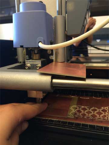
We machined using the Modela mini-mill at the IDC. First you had to place the brand new "small PCB" board (copper side up) on the modela bed. Underneath it should be a sacrificial plate so that if you mill too far down, you don't mill into the bed and instead mill into that sacrificial plate. Here you can see the board placed on the bottom left of the sacrificial plate. Instead of clamping, we use double-sided tape that covers ALL of the backing, or else you risk the board shaking and vibrating to the point of breaking a corner off.
Next you're able to import the designs for the boards. The trick here is that in order to run the fab module from the browser of the machine that is connected to the Modela, you have to somehow let it know that you are not invading the computer through the internet, so you need to open a script (saved on the Desktop) in order to let it commence the communication between the fab module in the browser and the machine connected.
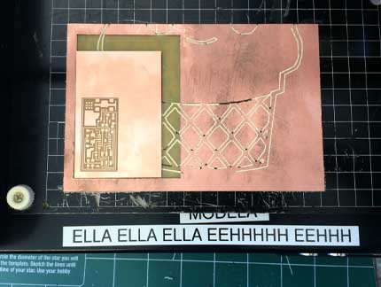
First we did the interior of the board pictured below left(actually the file called traces.png, )since this required not going all the way through with the 1/64" bit. This bit is extremely small and extremely brittle (if dropped), but otherwise real strong for milling copper off a surface.
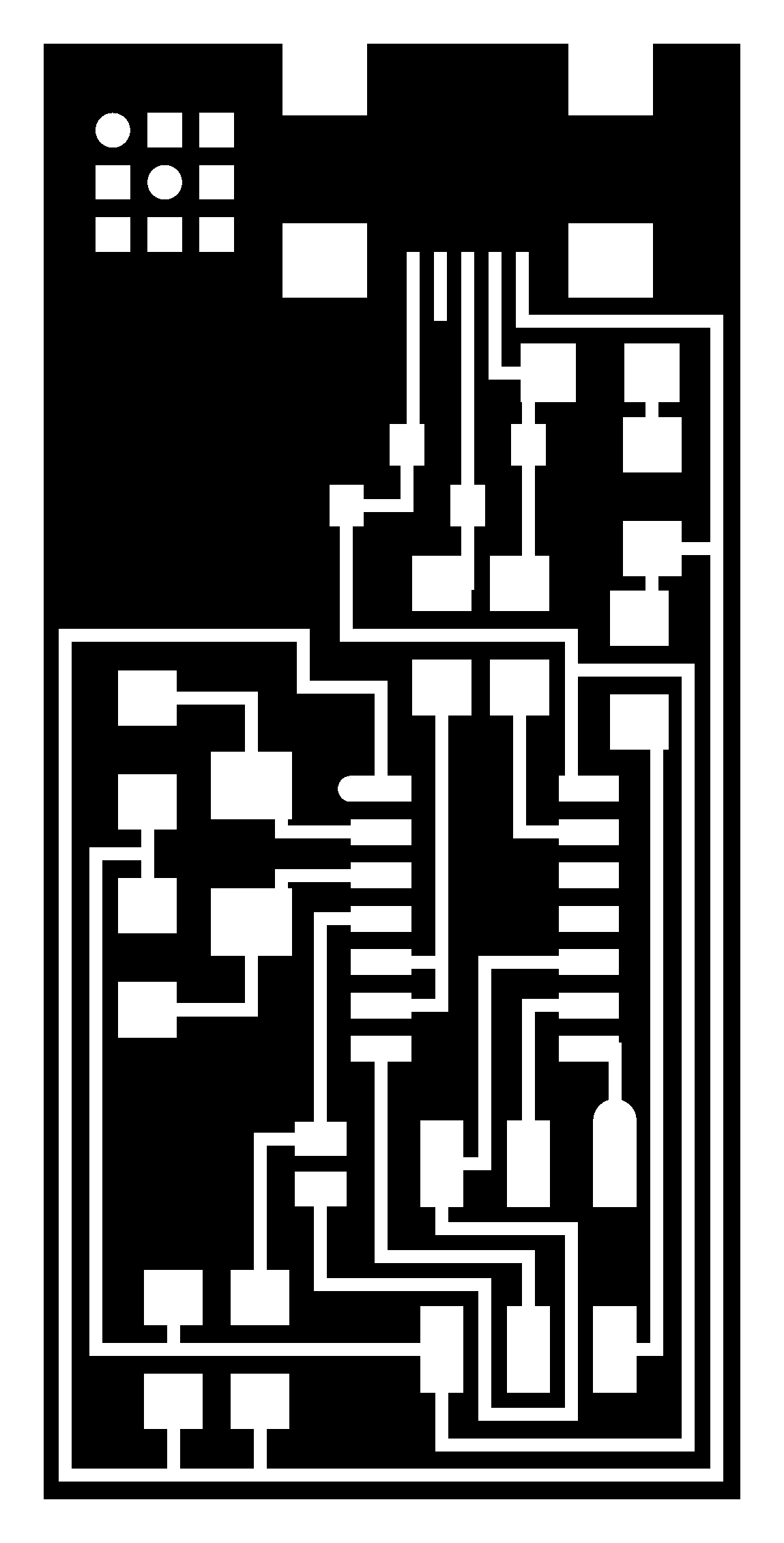

Next we cut off the board we need from the rest of the scrap of the PCB board we just milled from by loading the file pictured above right (actually called interior.png). You can see how it just perfectly overlaps with the traces file. Since now we're making a through cut to separate our piece of the board, we change the tool for the bit that is 1/32". You always want the bit in the chuck as deep as possible (less shaking and deflection of the tool), but you also want to make sure you leave enough space for the tool to come all the way down and cut through the board. A good rule of thumb here is to use the board as a measure of whether or not it can go low enough. Here you see me holding the 1/32" bit in my left hand (still loose inside the chuck) and measuring that there is at least a PCB's depth for the tool to still displace down enough).
After taking this picture I let the tip of the the bit slide within the chuck and tap the surface of the copper enough to remove any dust so that I know it's really zeroed in. Then I let the tip rest on the PCB surface, and tighten the two set screws in the chuck. Now I know I've got my tool zeroed and that it will definitely go down enough to cut through the board.
"Stuffing", or populating, the board
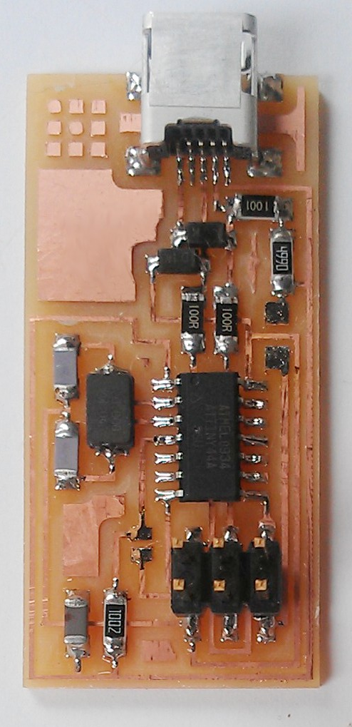
Guidance was a strong team effort here to figure out what each element meant. We had two pictures to relate back and forth: the circuit diagram on the left, and what the board was supposed to look like, on the right.
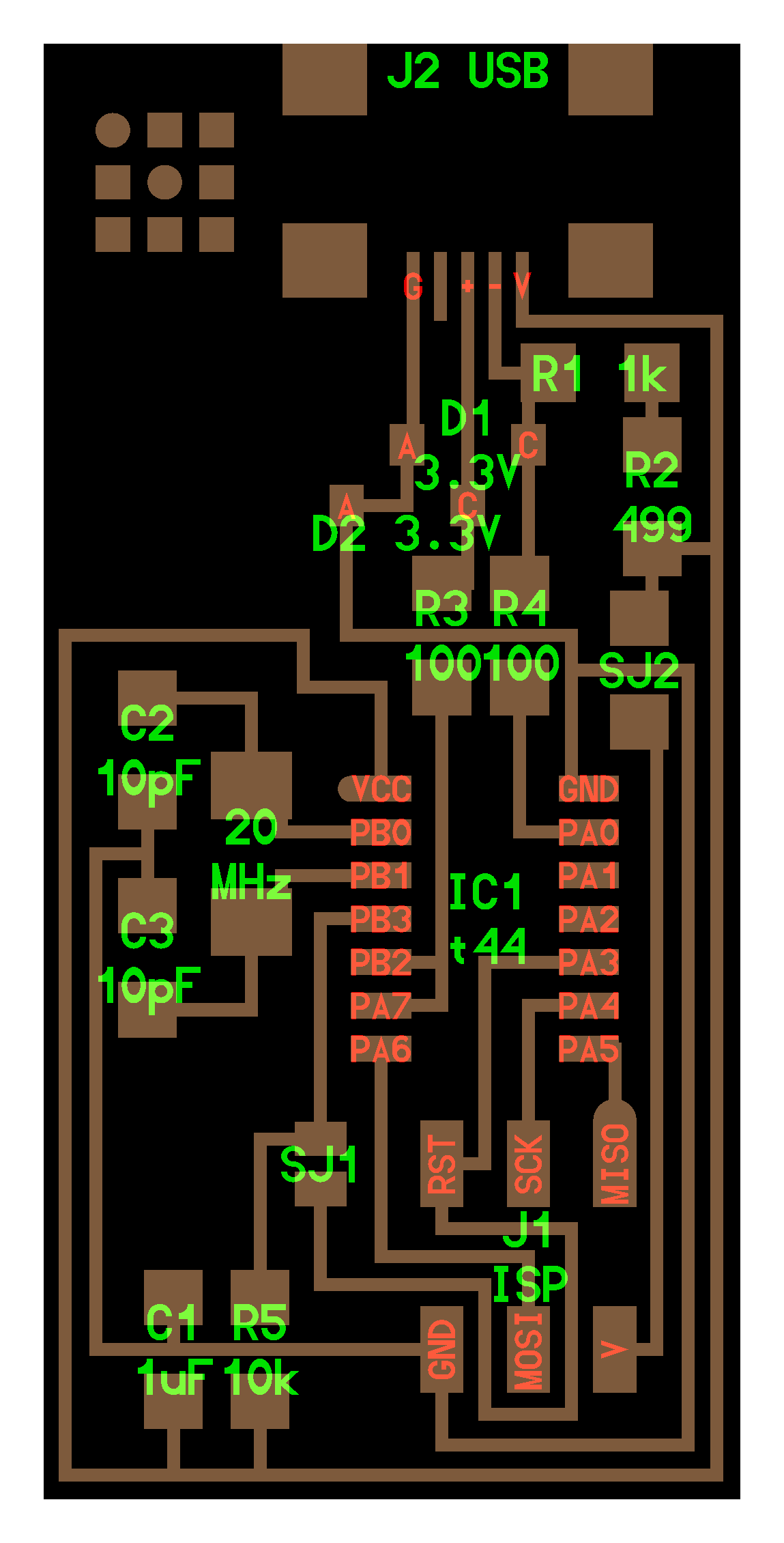
Going back and forth between these, with friends in lab with you, was key to identifiying the right component. It was all done pretty ad hoc, but You can find friend's pages that well documented the parts list and inventory of what you needed (See Anders or Rachel's pages). Subtleties like making sure you grab the Crystal 20MHz and not the resonator that's 20 MHz (or something like that) are absolutely essential.
Below you can see the transformation of my board with the progress steps: I started with the bigger components and worked my way down in size. This theory is supported by the fact that if you get these big ones too wrong, you might have to start all over. Thanks to some previous experience, soldering was not terribly difficult, you just needed the right amount of patience and speed. I had only ever done through-mounts, so these surface mounts were a fun and new challenge. We used the smallest diameter solder reel and the solder pen with the finest tip to do these teeny-weeny surface mounts. Also, the copper braid is your friend. Learn how to use it and embrace it. I recommend using an old board or keeping the one the TA makes during the tutorial and then cracks to use as practice in the soldering before you solder onto your own board.
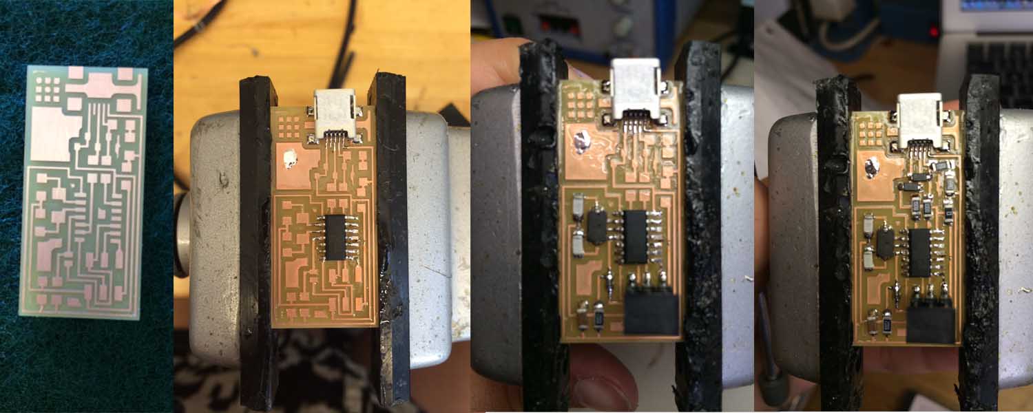
As you can see, my PCB has a beauty mark on it =).
Programming the ISP
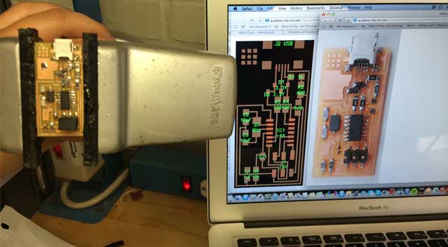
In this context, ISP means in-system program(mer). It's still unclear whether the board I made and soldered is the ISP or if the big box you see connected to it is the ISP. This programming was done at the last minute, when our class section deciphered that we did, indeed, need to program it our board (was not clear from the machining/soldering tutorial). As you can see, we were able to connect it to the big fancy box (this one was the AVRISPmkII) and have it shine red, implying that it recognized that there was something connected.
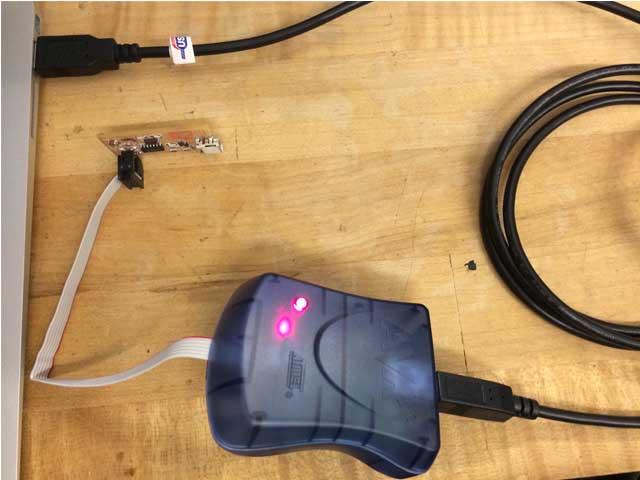
We met with some TA's and tried to program our board. We downloaded all the gear we needed, as per our fist tutorial, and we thought we were really close to being done, until we got this fatal error:
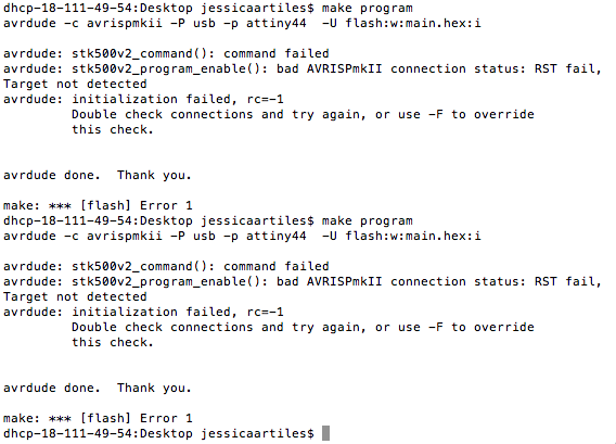
Kate and I tried debugging using another tutorial, but to no avail. Even when plugging in both boards, we still got the same error message. Ultimately, the TA, Michaek, and us threw up our hands and thought "we must need a mac guy" to help us debug the terminal errors.
Reflections
This assignment was particularly challenging in the communication of what was expected for this week's module to be completed. Electronics don't scare me as much as programming does, so it would have helped to have the programming instruction as part of the tutorial from the beginning to know what was expected of us. It was nice to not have to think about designing the board, but rather just focus on how to make the board and gain practice soldering (and time to enhance our websites!) I only wish I had some more intuition from the manufacturing process to inform my design of the PCB in later weeks.