Pranam Tries To Make Things
MAS.863 - 2016
Week 4: Electronics Design
Designing an ISP PCB Board with an LED and Button
Darn. Back to the horror show that is eleftronics! This was my chance to get used to Eagle. Using Eagle was my first real experience with PCB design, and it was, well, a learning experience. To do this week assignments, I went to the links provided by past students' pages. One of my favorites was this SparkFun tutorial!
Using this tutorial, and just looking on pages, I was able to design a schematic diagram. I started the board by inserting all the components from the original Hello World PCB into my schematic editor, and added an LED and button. I had to make sure they were all in the Fab library, which I sourced from.
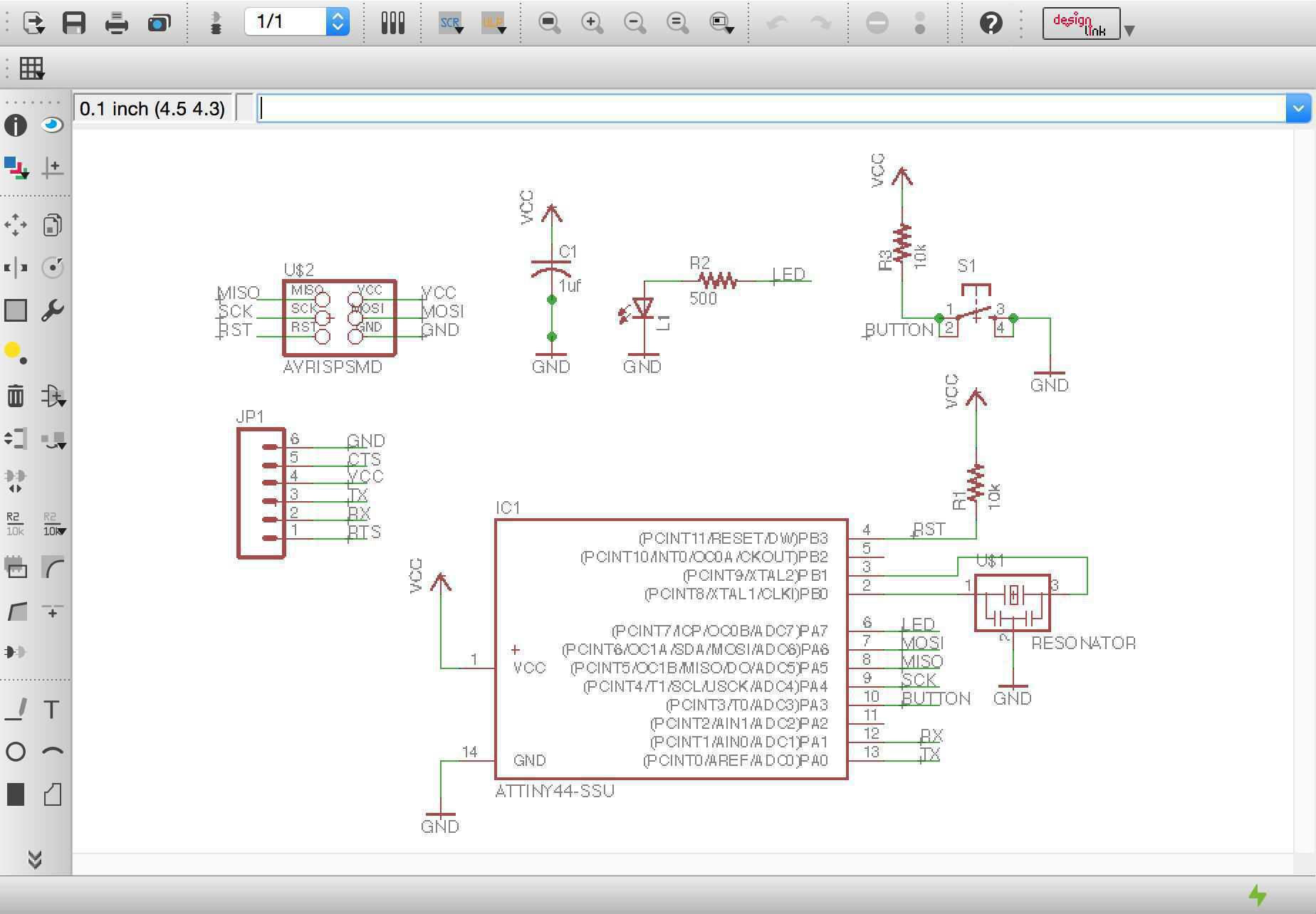
Figure 1. Eagle Schematic of Board.
Next, I switched over to align the board, which was the most troublesome part of the process. Routing the connections in board interface was a pain. I tried to make all the routes as clean as possible, by following TA Ben Jennet's page!
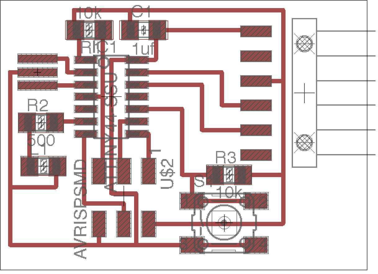
Figure 2. Routing the board in Eagle.
Once I did that, and then made the outline on a separate layer using a wire, I exported both the top layer into a PNG for the trace, and the bottom layer (20) for the outline.
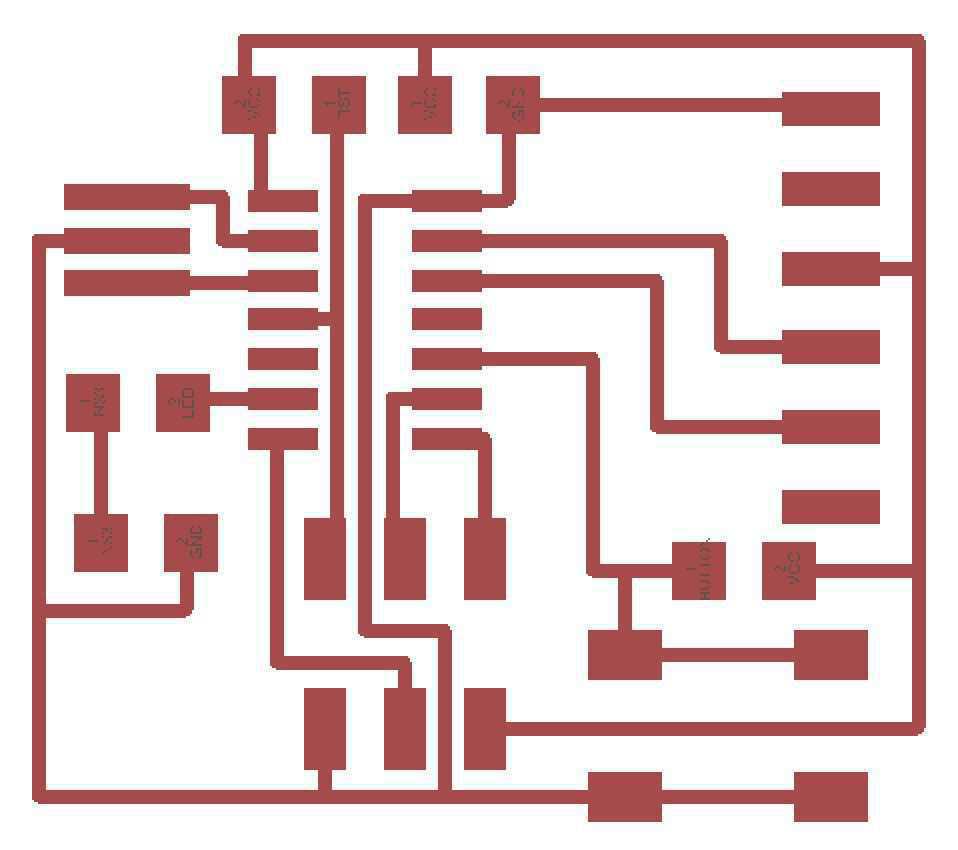
Figure 3. Top layer of the board, before exporting it as a PNG.
Next, my least favorite part: milling. Gosh, I hate this. I always fail. And this time I did again, because I first forgot to invert the PNG. Then after I printed one board, I realized that my dimensions were too big!
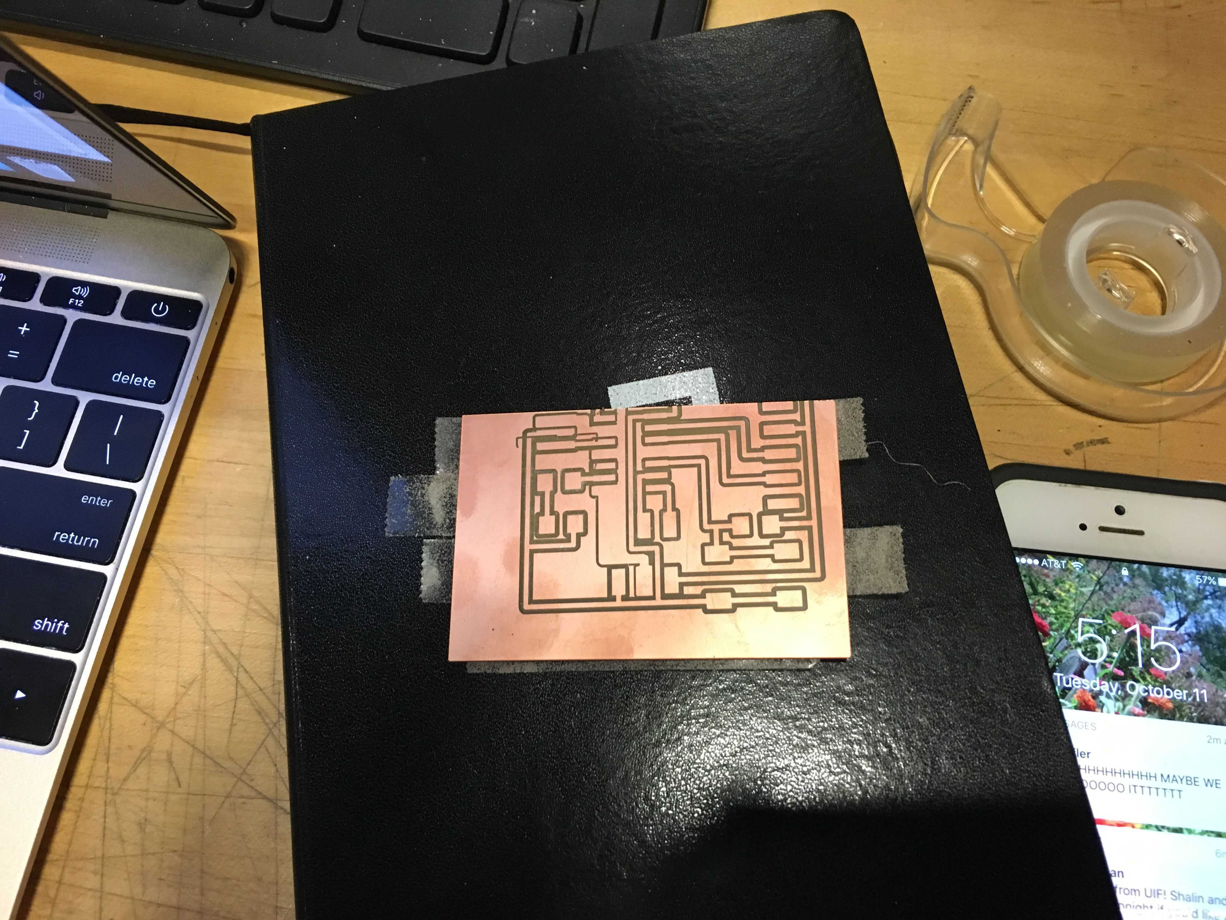
Figure 4. Failed milling of board due to too large dimensions.
The problem? MAC! SILLY MAC! Classmate Hisham was awesome and exported my files from his Windows computers and they were the right dimensions (about 1.3x1.2 inches). Finally, I could mill the board correctly!
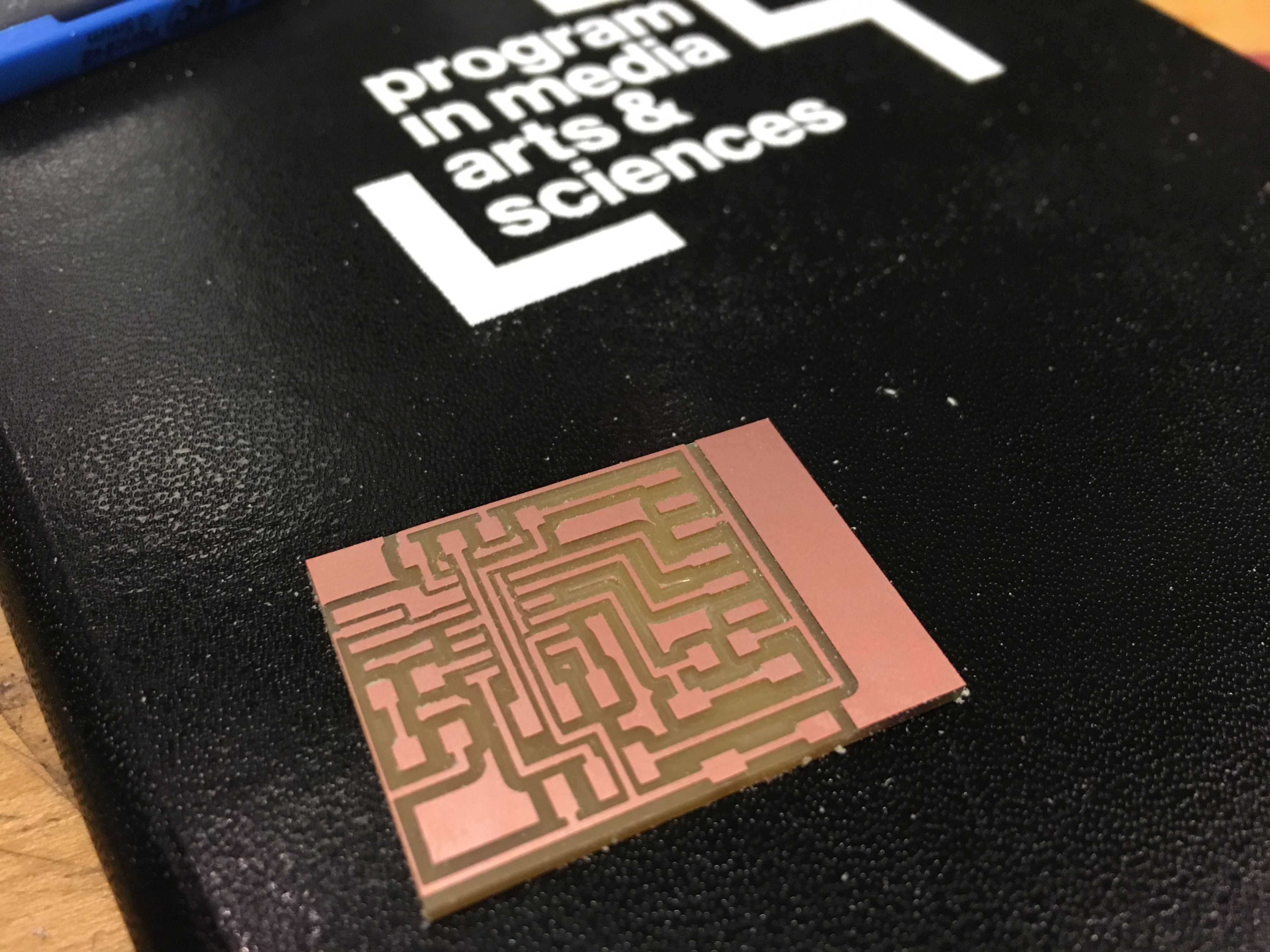
Figure 5. Milled and cut PCB Board.
Finally, at 2 am of the assignment due date, I was able to stuff the board, which was not difficult, as I did before. However, as I was very tired, I didn't get a chance to test it. I will do so before next week's class. Since I won't use this board for any specific purpose, I will try again with a meaningful board for my Final Project, where I design a photogate.
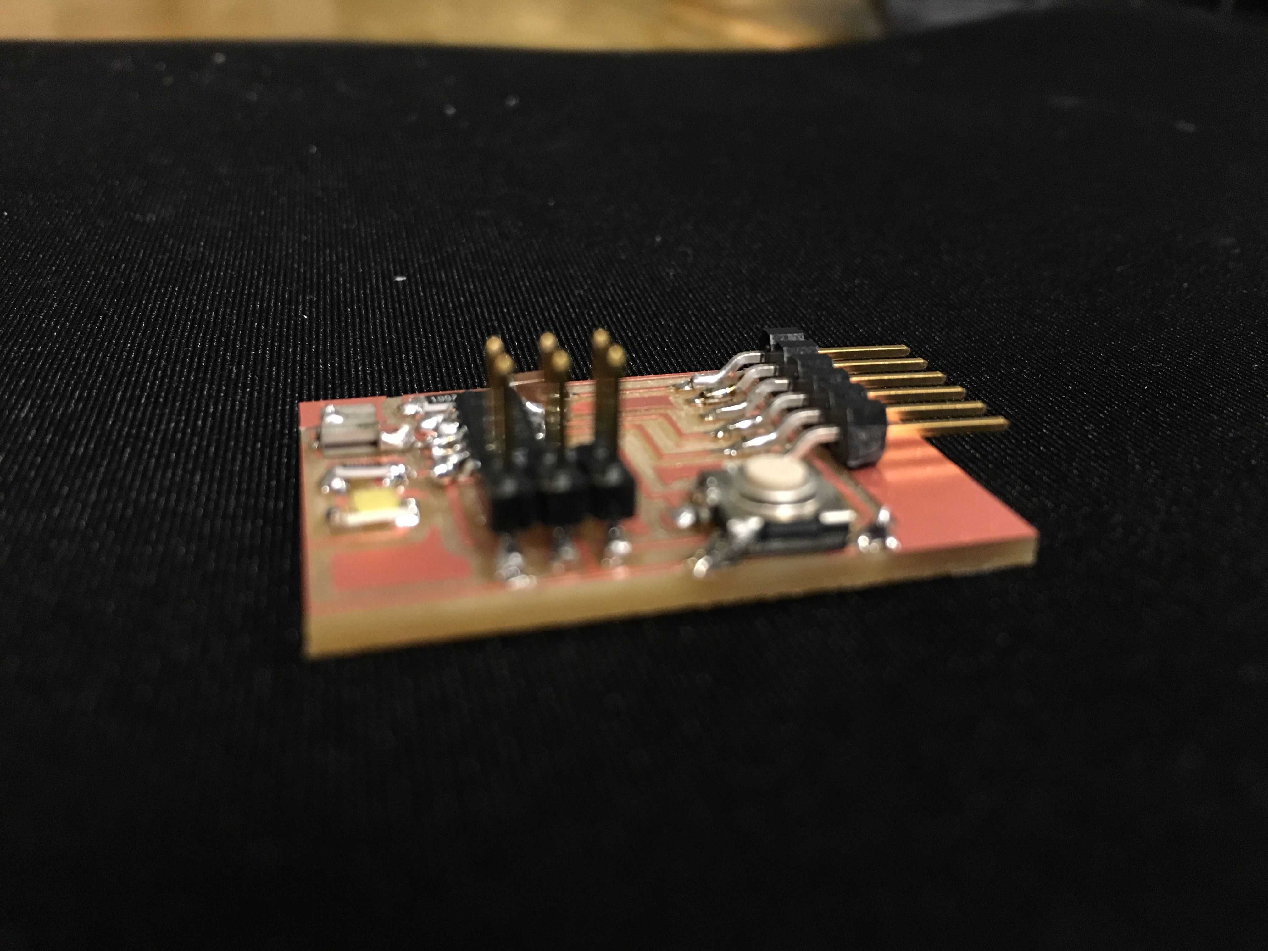
Figure 6. Stuffed board.
| Activity | Tools Used |
|---|---|
| PCB Design | Eagle |
| PCB Milling | Modela |
| Board Filling | Soldering Iron and Flux |