Pranam Tries To Make Things
MAS.863 - 2016
Final Project
The FabSpec
Introduction
As a synthetic biologist and genome engineer, I am always looking for new ways to not only better the systems I build, but also make more efficient the worflows I use to build them.
A great portion of the experimental work for synthetic biology deals with DNA assembly, where we piece together different segments of DNA all onto one vector to express our systems in different settings. To do this, we have to transform bacteria with our plasmid after construction, so to propagate the assembled DNA, and thus have higher quantities of it to use in various scenarios. Thus, growing healthy bacterial cultures is very important for synthetic biology.
The appropriate way of maintaining healthy cell cultures is to use a spectrophotometer, which can allow biologists to monitor cell density. Commercially available devices are not designed with rapid prototyping goals (such as gene editing tool development or synthetic circuit characterization) in mind and as a result tend to be either too large, costly, have inflexible software, and worst of all, require molecular biologists to constantly do manual checks of cell density. Here, I propose to use the various modules to create a cost-efficient, realtime wireless spectrophotometer: the FabSpec. The end goal will be to provide molecular biologists with reliable, realtime notifications of when bacteria is ready to be harvested for DNA extraction through continuous monitoring.
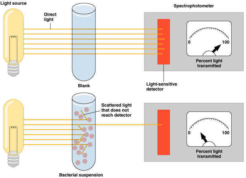
Figure 1. A schematic of a spectrophotometer.
3D Modeling and Apparatus Design - First Iterations and Prototypes
We began the How To Make (Almost) Anything class with a CAD module! I downloaded a multitude of softwares, and even the easy ones made no sense to me. Luckily for me, I chose the easy-to-use, non parametric software: Rhino. I thought its interface was intuitive, and I could "see" my model coming to life in it, but man is it confusing at first. Tom was able to help me through it, and now I am a Rhino master.
So, back to the project: the FabSpec. The main 3D model is a tube-holding chamber that can be emcompassed by a circuit for a spectrophotometer integrated measurement device, basically a photogate. Here's my rendition of it:
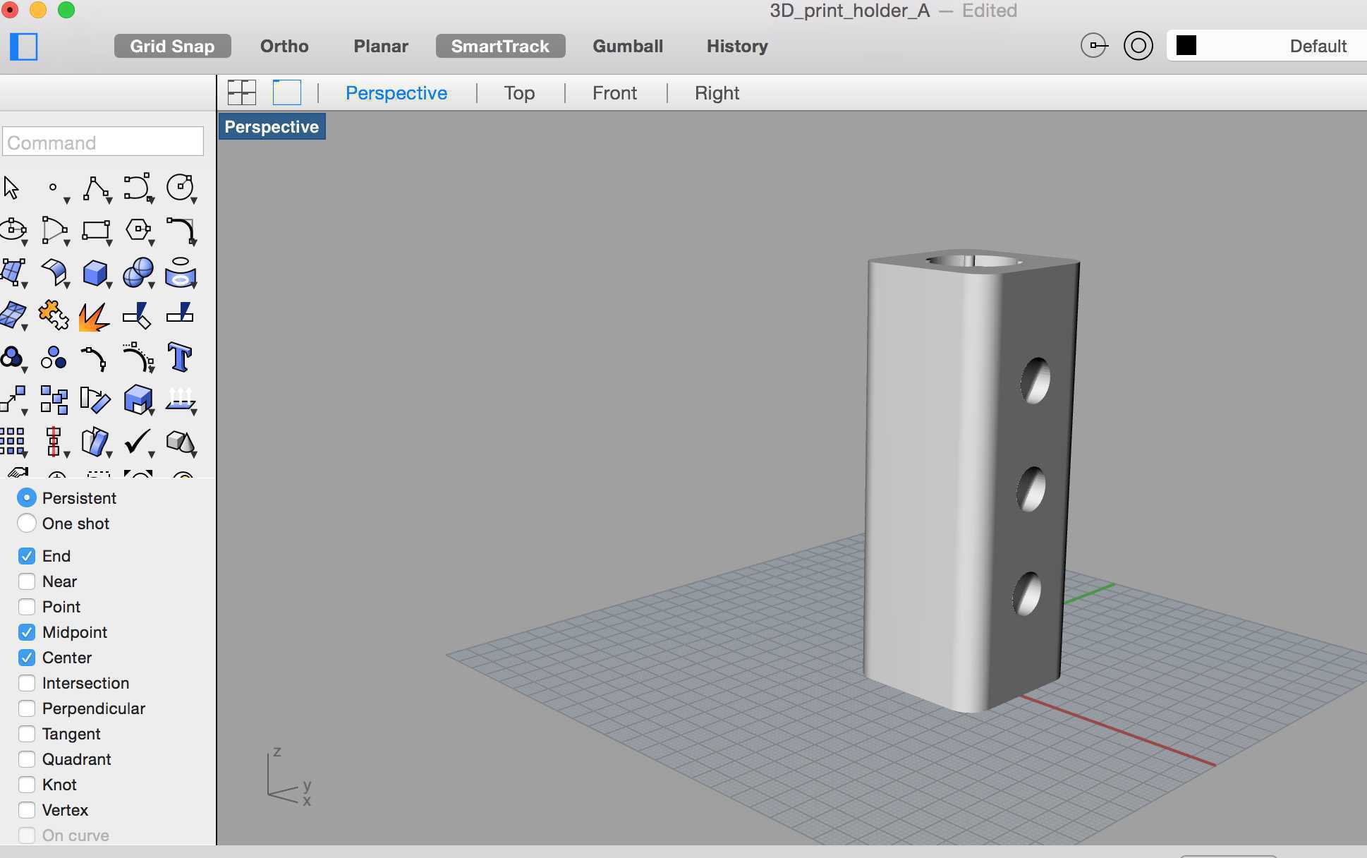
Figure 2. A Rhino model of a cell culture tube holder. The holes will allow for photogate measurements.
I sent this file to Tom to 3D print downstairs in the CBA shop!
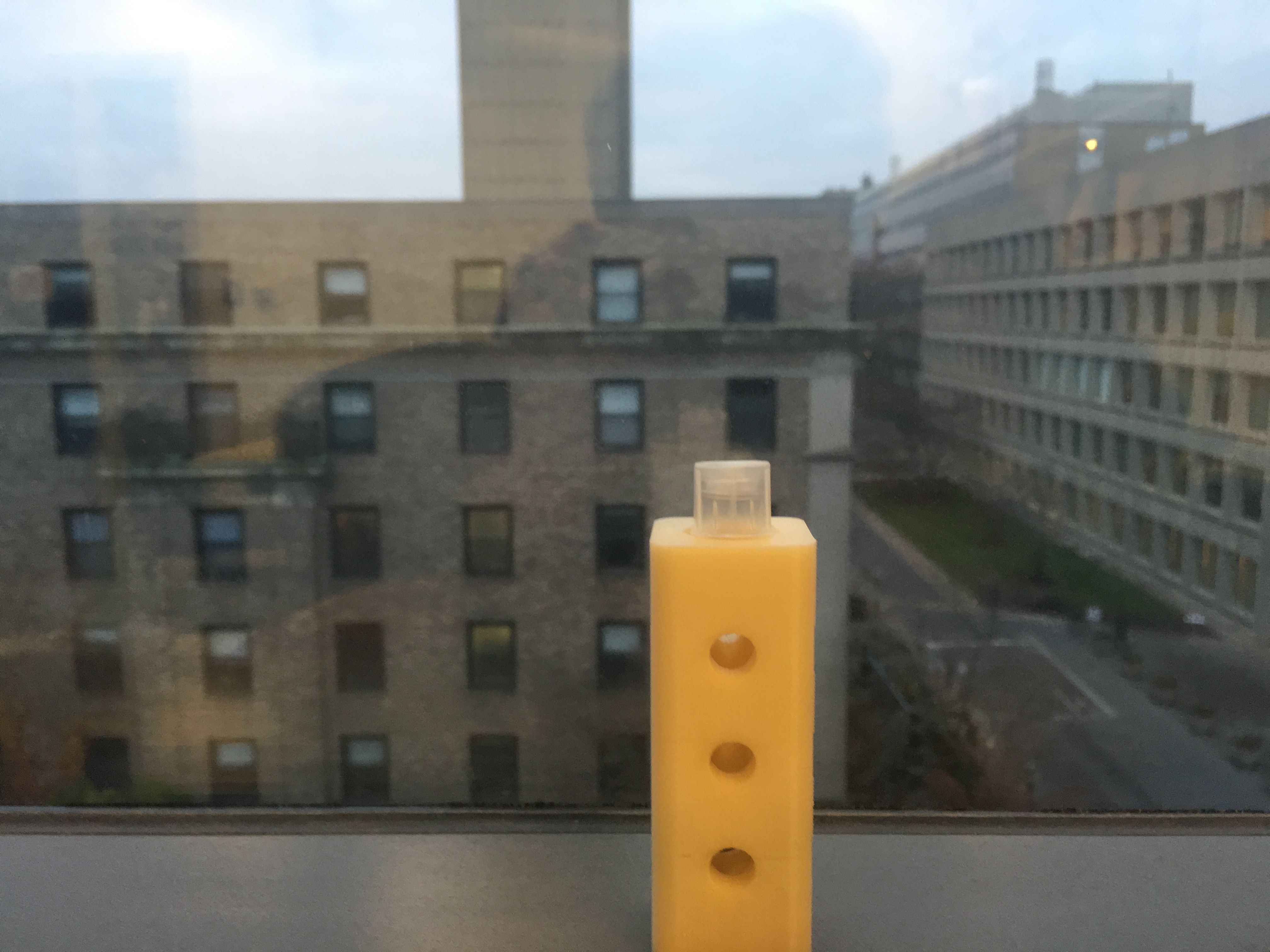
Figure 2. The 3D printed tube holder, holding a tube.
Next, the idea will be to laser cut the stage to hold all of the circuitry on. Since this is a spectrophotometer, I will need a two-sided stage to hold both the LED on one side and the phototransistor/receiver on the other. Thus, I made a simple 2D layout on Rhino that I plan to cut using acrylic.
Figure 3. A Rhino model of the circuit stage.
Finally, the tube holder will attach to a base which can be placed (and balanced) in an incubator. The 2D dimensions of the tube holder is 30 mm x 30 mm, with filleted edges, so an inserted square to attach the holder should be fine.
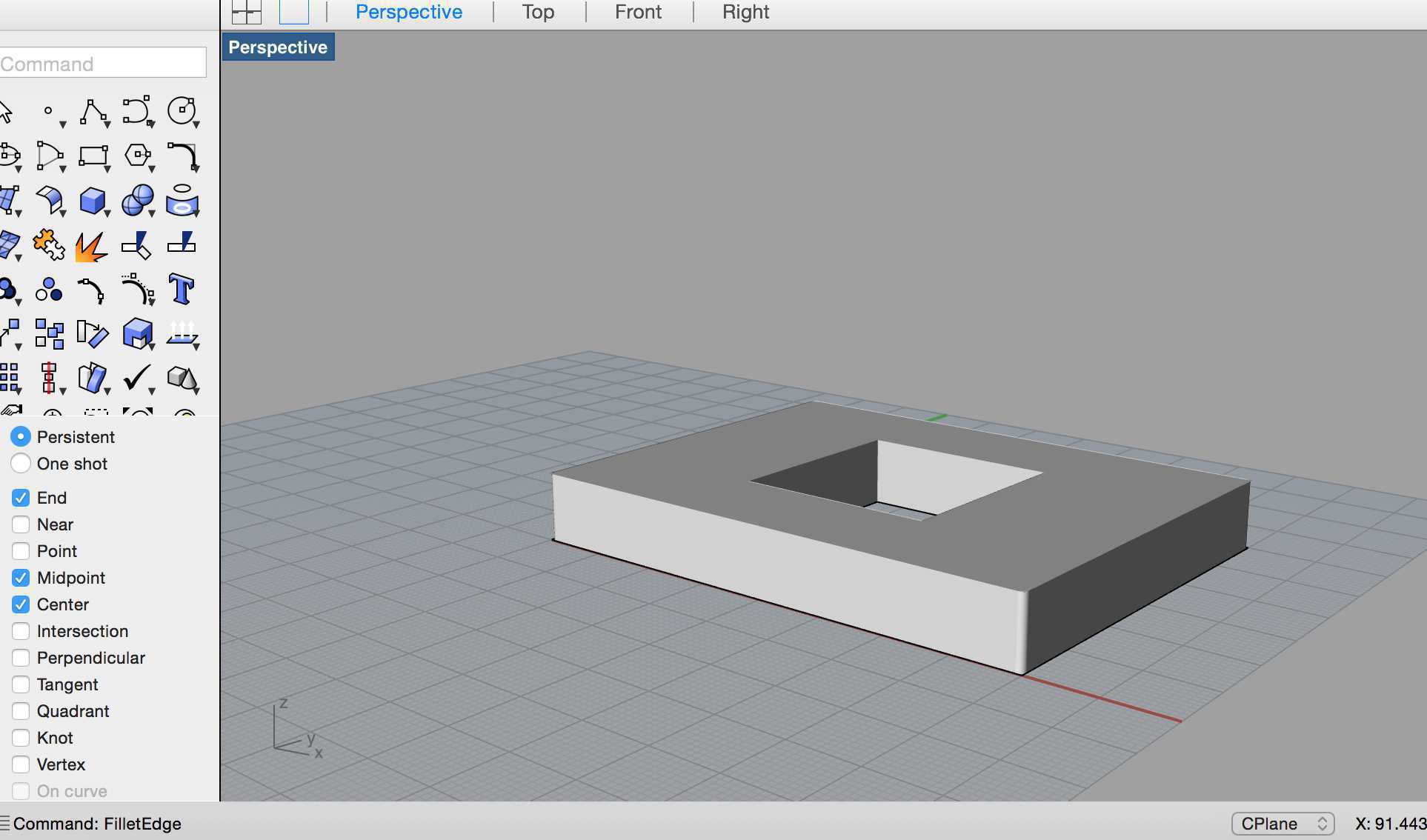
Figure 4. A Rhino model of the apparatus base.
I was able to finally get through the molding and casting stages, learning how to create a ShopBot toolpath, milling a wax mold, pouring Oomoo, and then liquid plastic. The base fit perfectly in the end, though it's probably too small for the final version.
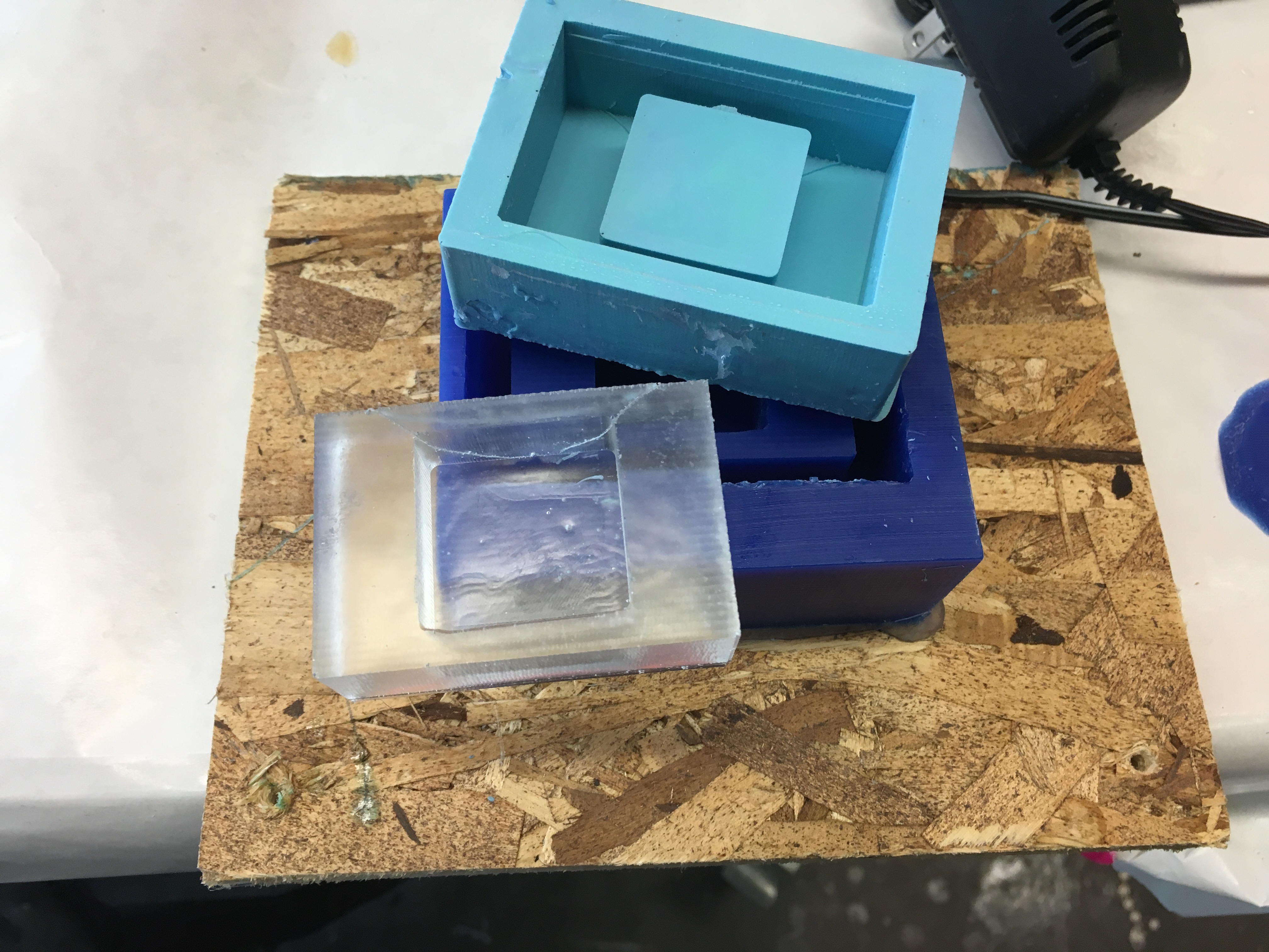
Figure 5. Molded and casted base!
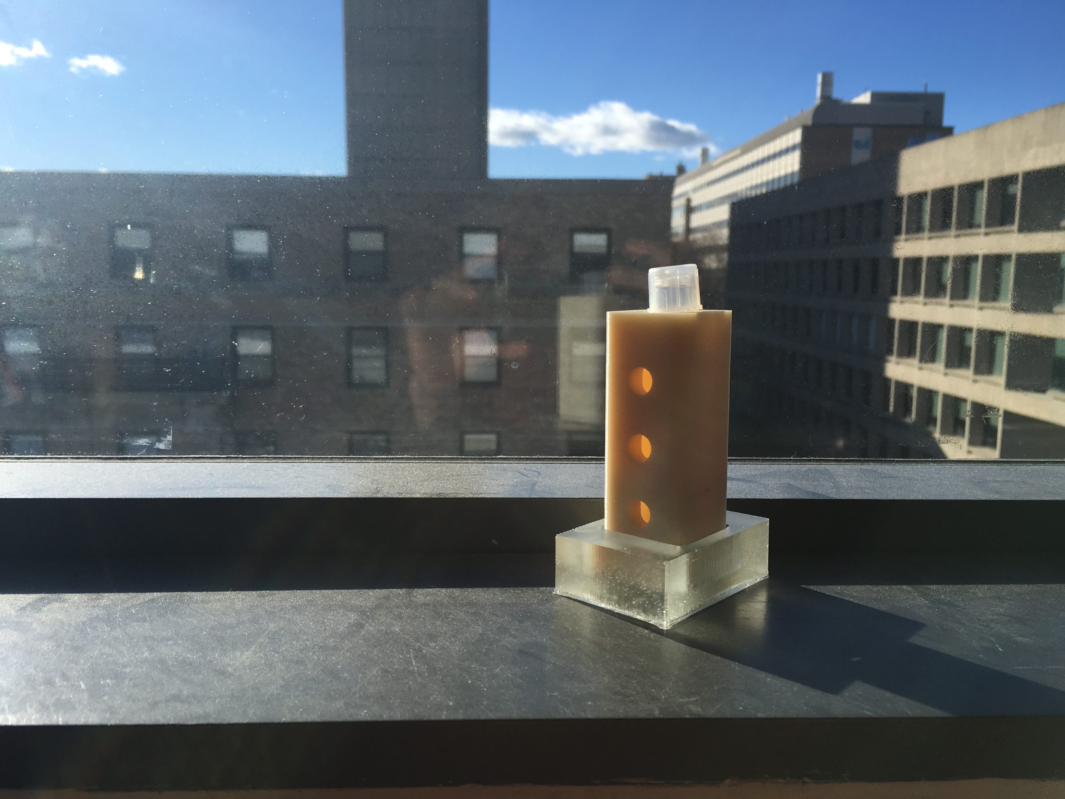
Figure 6. A perfect fit with the tube holder.
Electronics and Communication Initial Ideas and Prototypes
Next, the goal was to design a photogate circuit in Eagle that will measure cell density, and be able to read it out to a computer. I spent a long time figuring out a good design for the photogate circuit. The final iteration was to have a 9 V battery powering both the 5 V ATTiny microcontroller through a 5 V regulator, as well as a bright white LED (indicated by a transistor since I need through-holes). On the other side, connected to an ADC pin, is a phototransistor, which can read the amount of light passing through a tube, and gate that as a voltage value
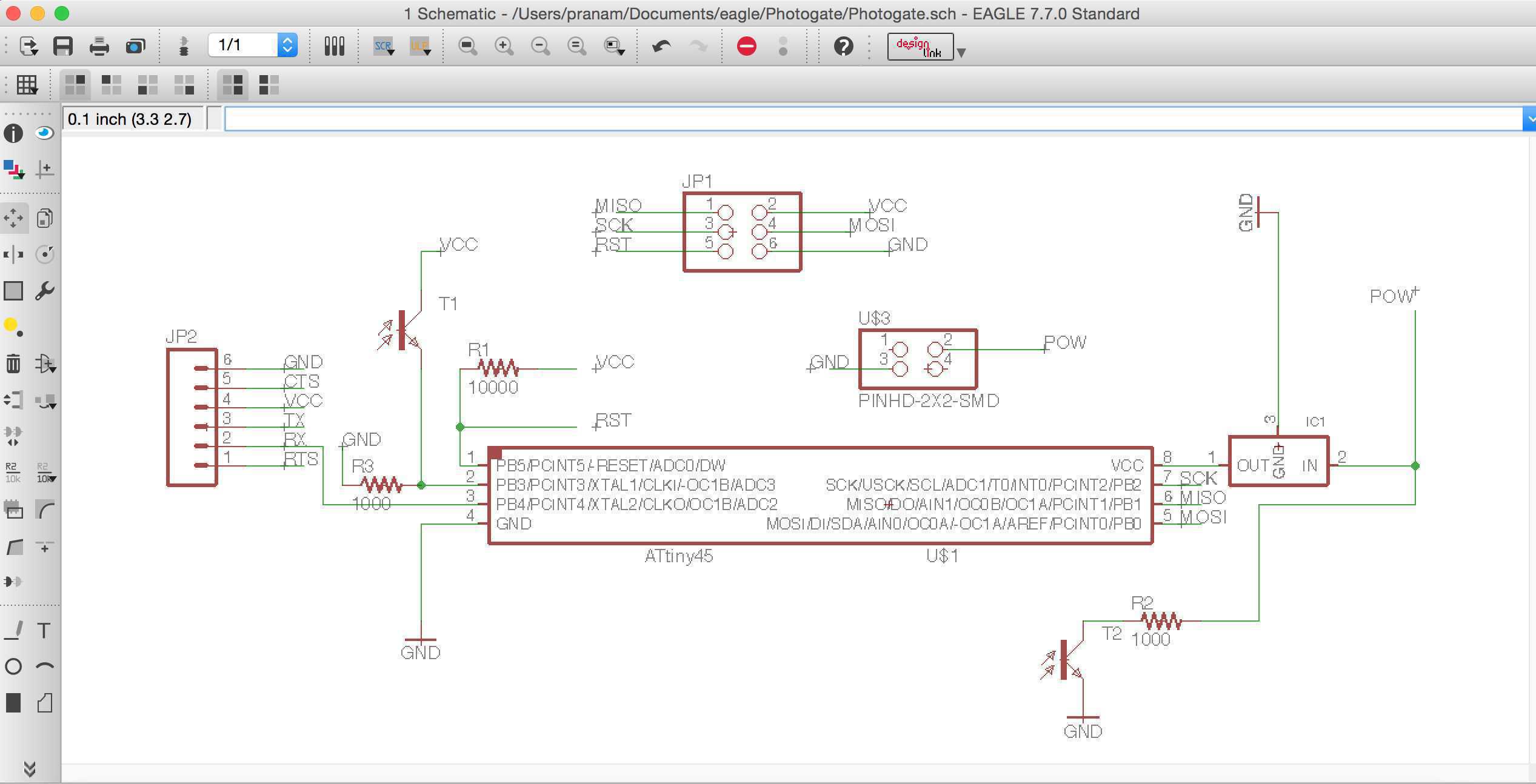
Figure 7. Eagle schematic of Photogate.
Then, it was time to route. With so many connected components, I took Hisham's advice and took a guess at the orientation of the board that would yield the fewest overlaps, and then used the best autorouter design. I settled on a design that needed only 1 0 ohm resistor. The next iterations, I may need to reroute the board so that it encompasses the tube holder. I probably can cut the middle with the laser cutter!
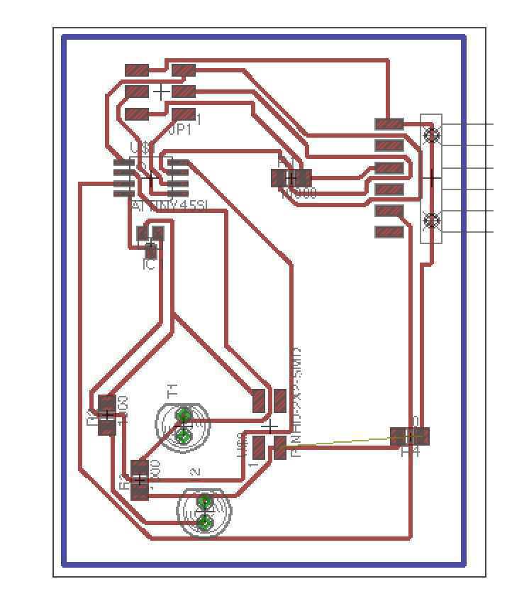
Figure 8. Eagle board design.
The plan is to program it with the following short C code application I wrote. This is just a starter program I wrote from scratch. Basically, I read in the voltage from the photoresistor every minute (no need to monitor it for too long), and then I store the value in an array of fixed value (perhaps read voltage every minute for 1 day), and then export the array as a CSV, which can be opened by MatLab or Python and graphed for the user to see. I may or may not use this as an output reader, but it doesn't hurt to have options!
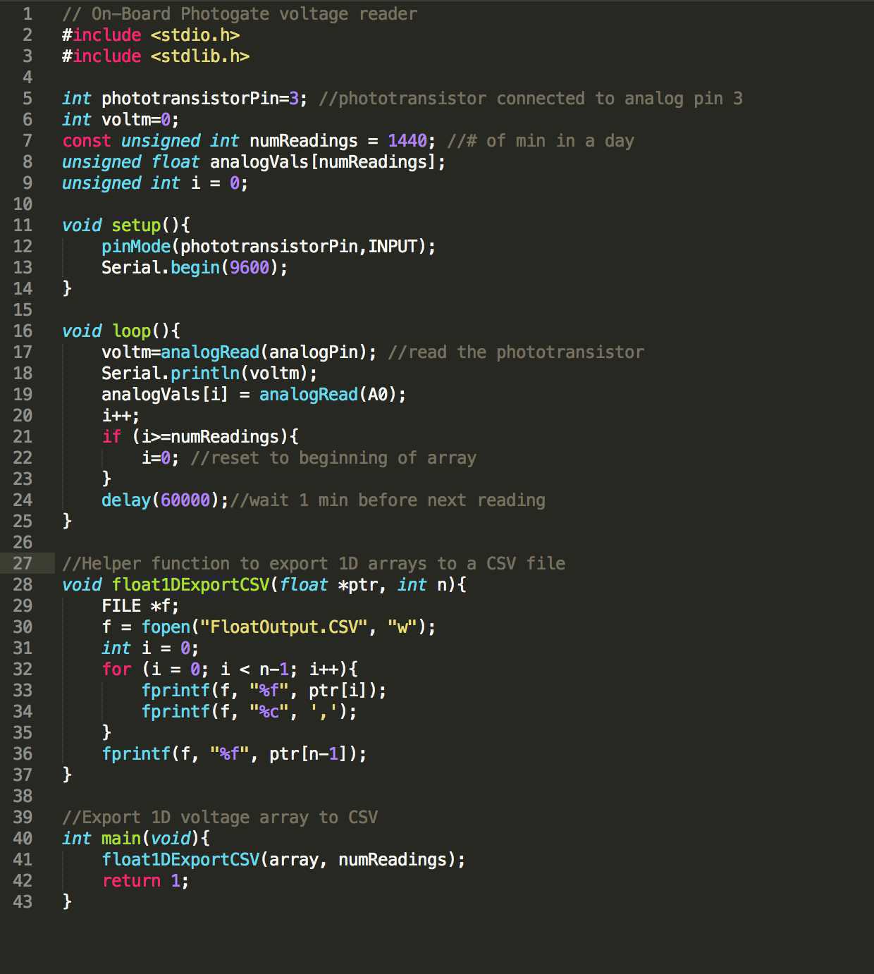
Figure 9. Program to interface with FabSpec.
So instead of a simple graphical representation on the computer, a potentially cooler, more interesting idea that deals with Networking and Communications will be to add a Bluetooth Low Energy module to the board that can read voltage data to a molecular biologist's cell phone, telling them when bacteria in a culture tube is ready to harvest and extract. In actuality, not much needs to be changed to the board, other than to have the FTDI header's TX and RX pins be connected to the microcontroller. But to do that, I have to use an ATTiny with more pins -- on to the ATTiny44! Just as a note, I decided to separate the LED board from the phototransistor board, so to spatially arrange the device in a clean manner. The 9V battery will still connect to both boards, but with parallel wires.
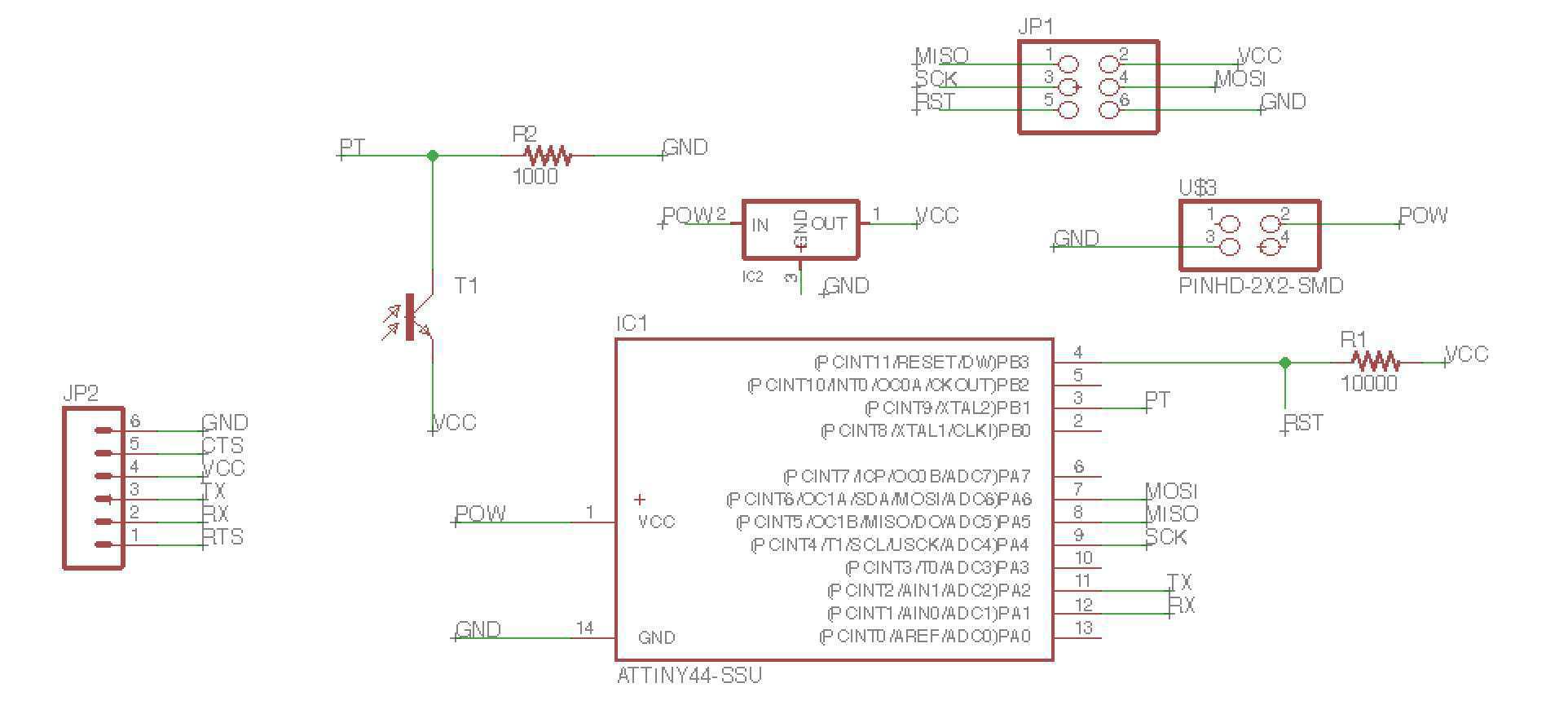
Figure 10. Updated phototransistor schematic with TX and RX pins connected to ATTiny44.
After designing, I went back to the autorouter, and got a nice (but weird looking) arrangement that I will to mill and stuff.
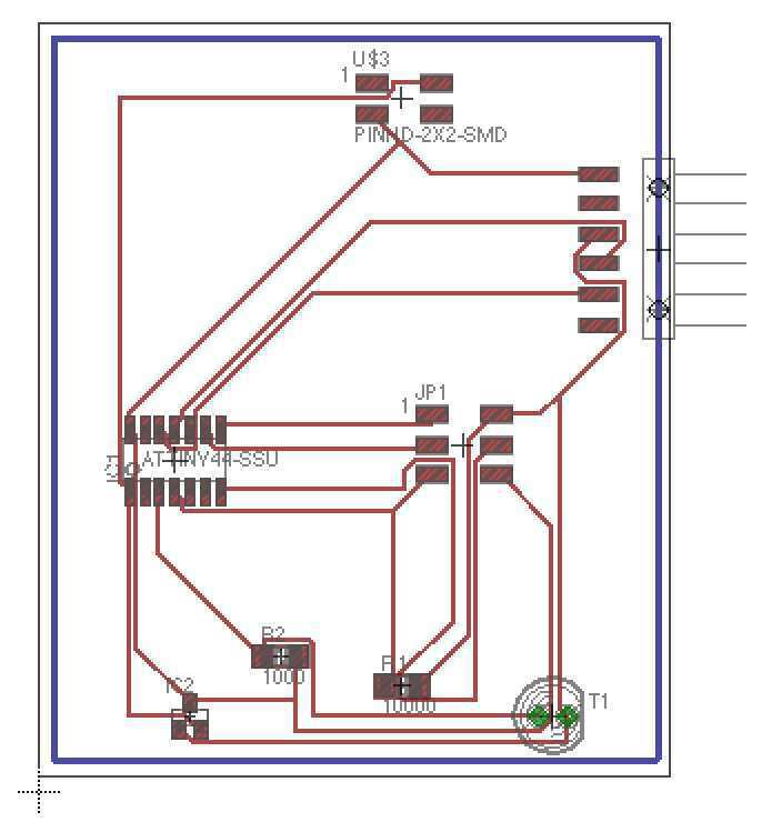
Figure 11. Autorouted phototransistor board.
The plan is to use an HM-10 BlueTooth Low Energy module that can connect to the 5 pin header, as mentioned by Thras in a recent email to the CBA section. The idea will be to do a Bluetooth connection between the low energy module and the bluetooth device in my iPhone, which can be read by a simple Bluetooth communications app already available on the App Store like LightBlue Explorer . These modules that I can attach to the board will be available soon.
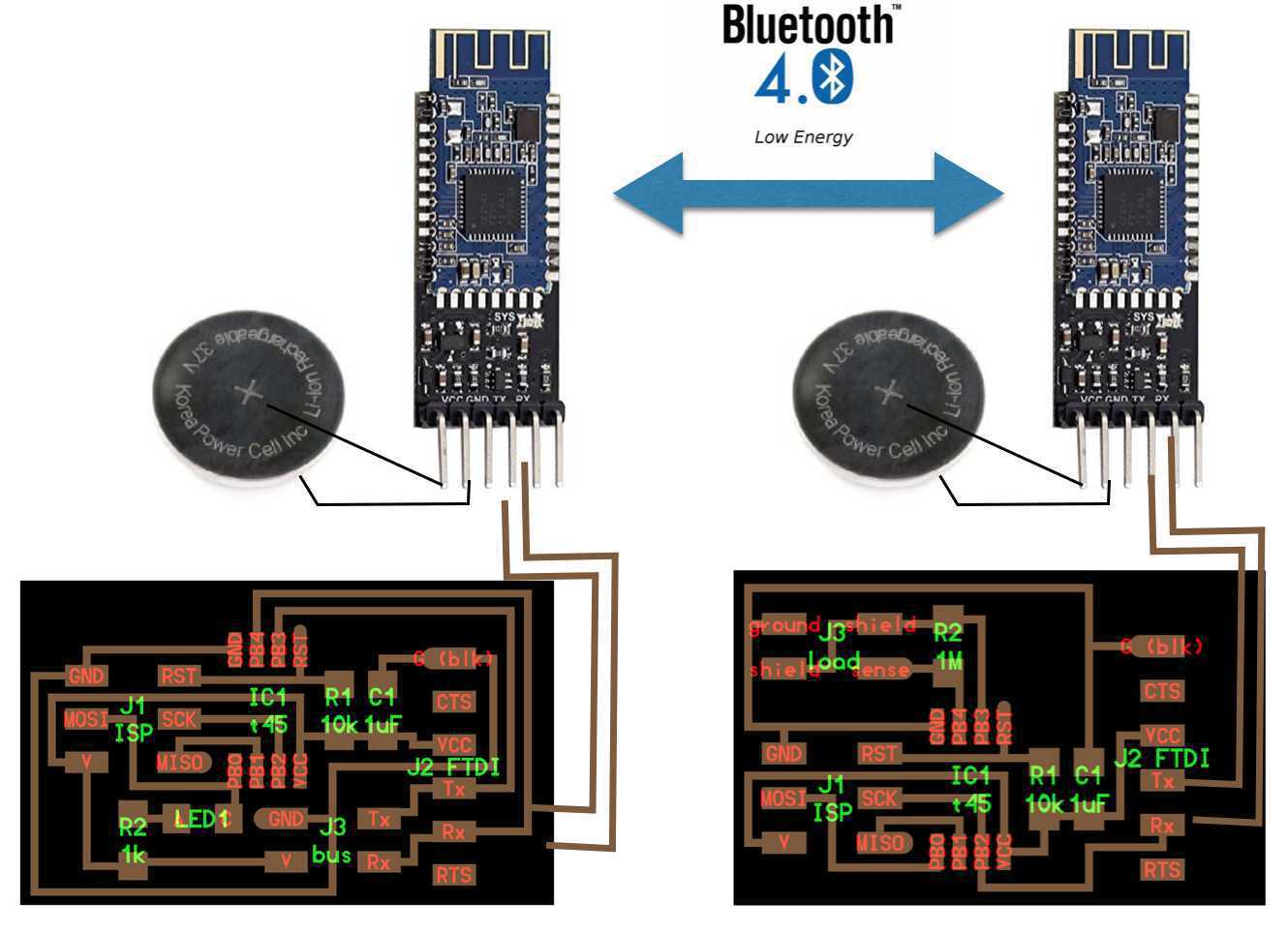
Figure 12. Hello World Bluetooth demo.
Final Designs
Whoa, that's a lot designs, ideas, and initial prototypes. Now, it's time to converge on specific designs. Here, I will present to you the final designs for the apparatus and the electronics. After this, I will be fully committed to building, prototyping, and testing these designs in preparation for the final project presentations.
Let's start with the apparatus. I decided to stick with the integration of the building modules: 3D printing the tube holder, molding and casting the base, and laser cutting an enclosure for the circuitry. The 3D print is done, and it's great. I will work with this model. As for the base and enclosure, I decided to create a press-fit design. The walls of the enclosure will press fit with each other AND the base. Thus, I needed to redesign the base for another mold and cast.
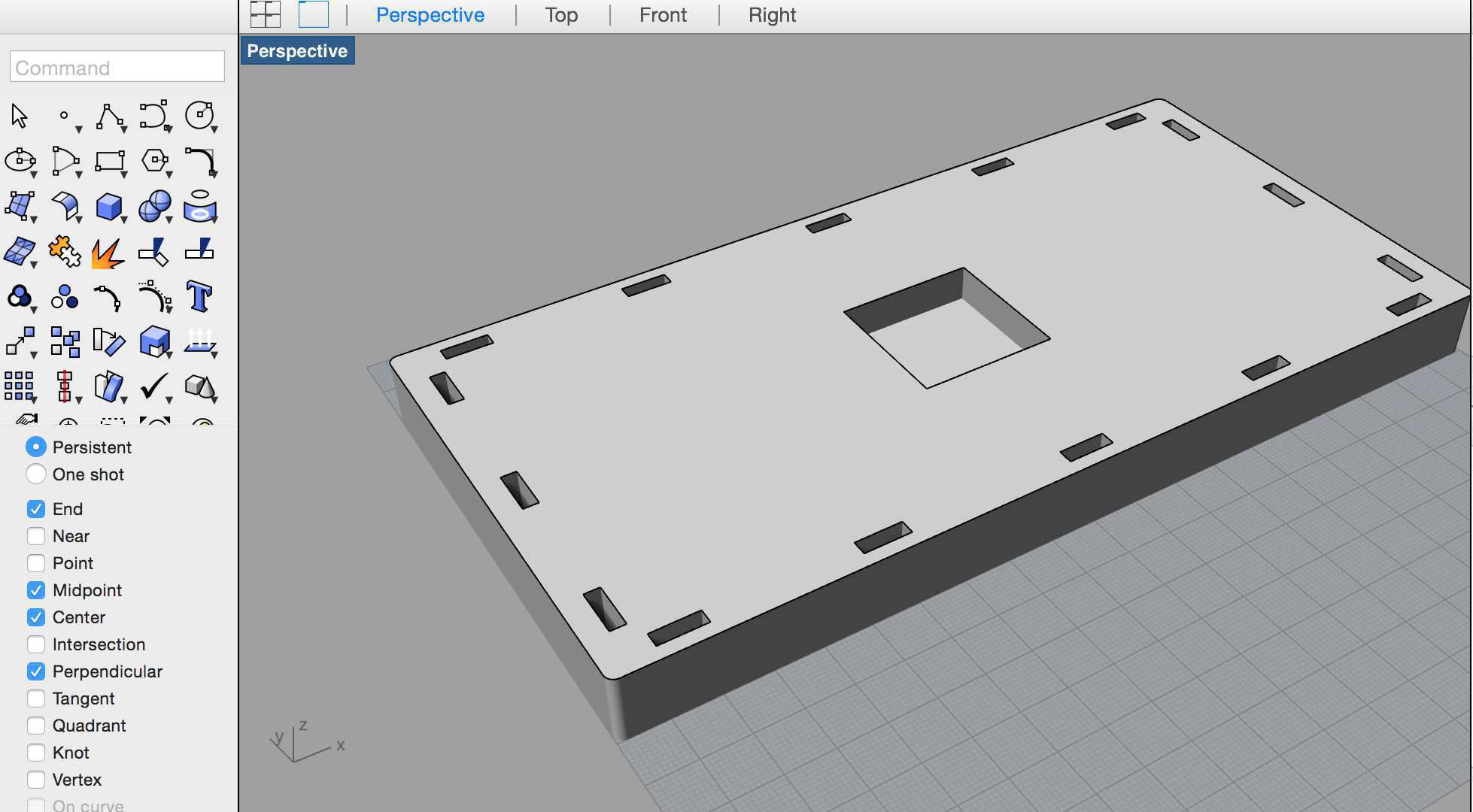
Figure 13. Rhino model of press-fit base.
I have already created the toolpath, and will mill, mold and cast it very soon.
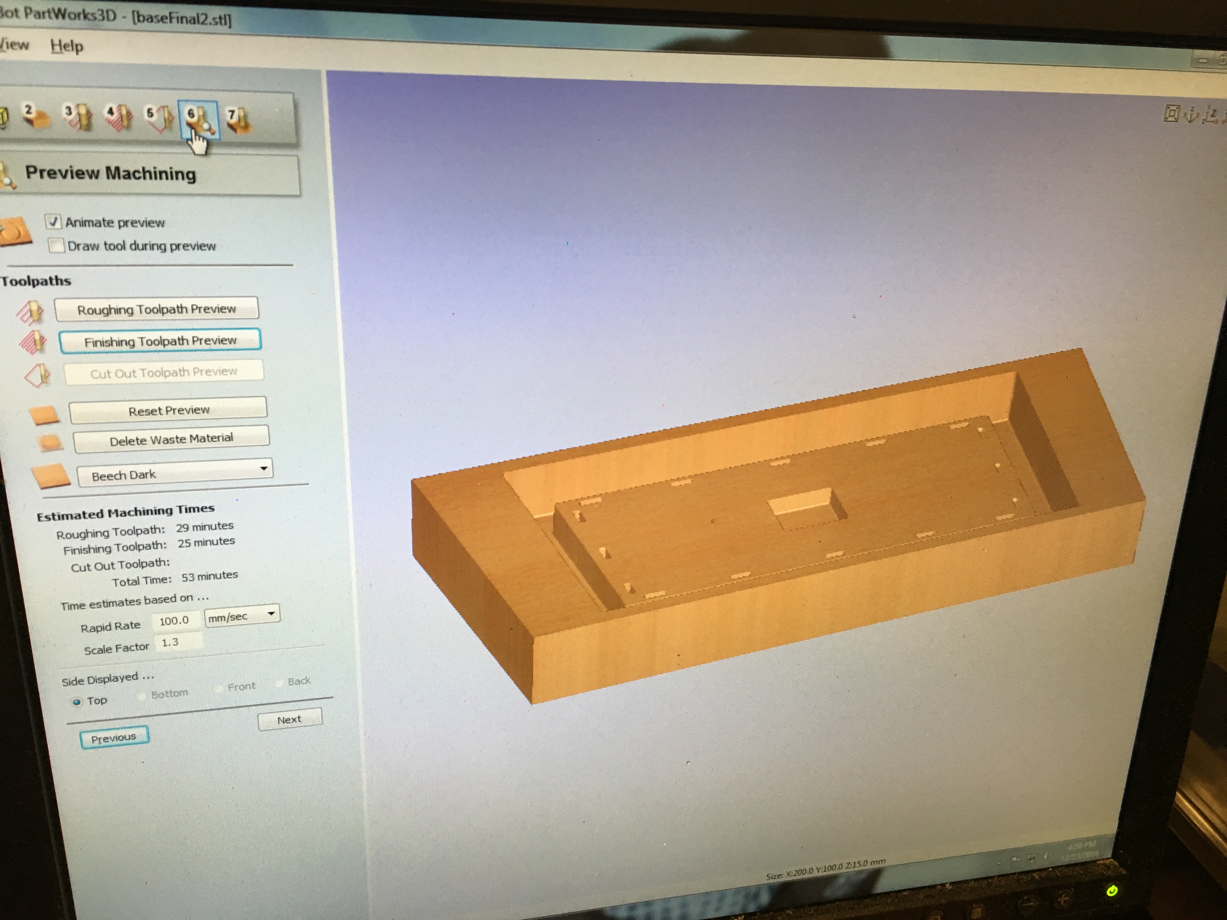
Figure 14. Toolpath of press-fit base.
Based on these dimensions, I designed 2D models of the enclosures, which will be cut with 0.125-inch-Delrin material, whose opacity will block external light from being detected by the phototransistor. I did a first design and cut, but this was for a different base design, which has been changed to the one above.
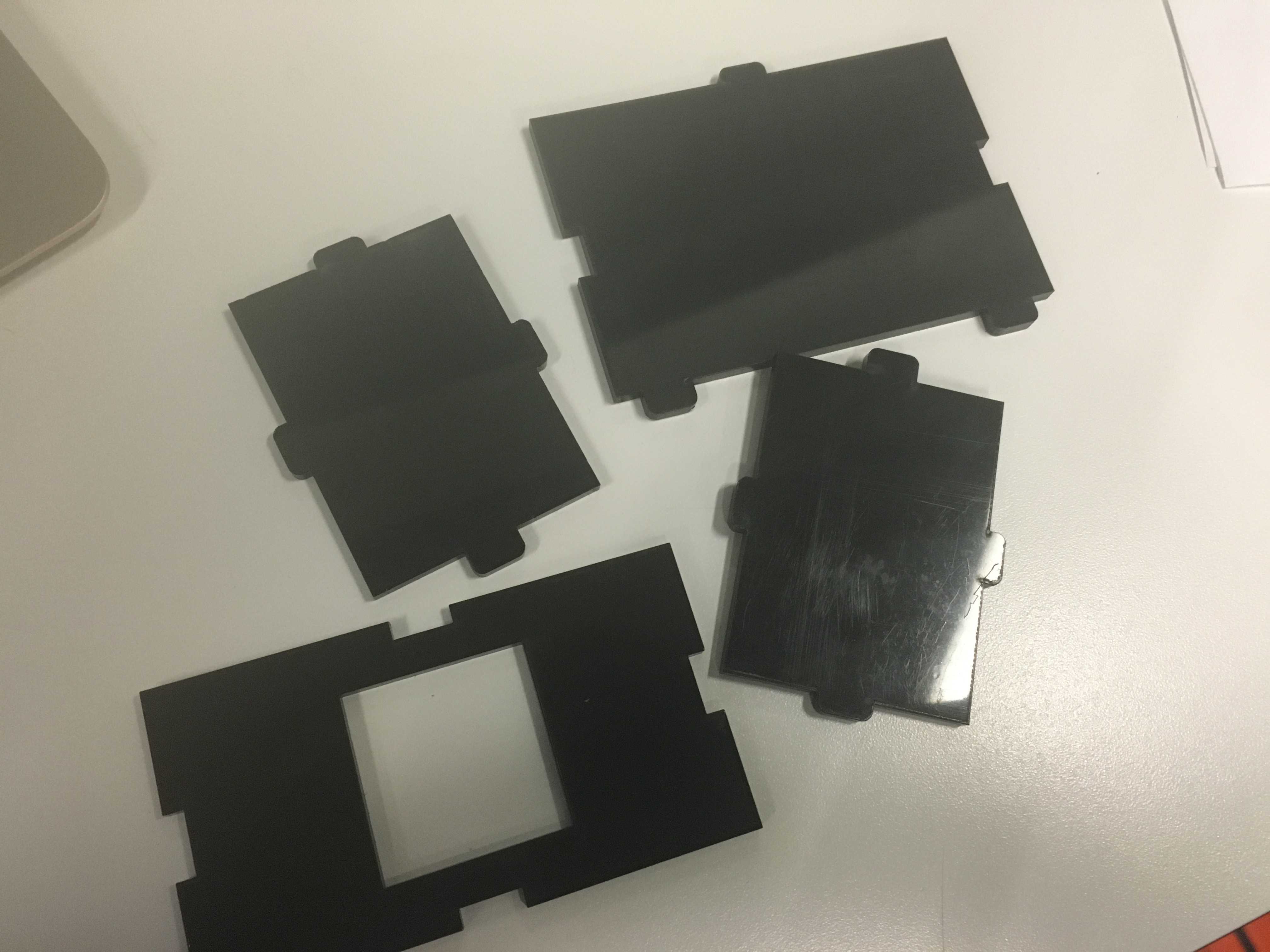
Figure 15. First laser cut with Delrin.
Now, however, I have designed the appropriate enclosure walls, which will allow for a big base, and area to fit the electronics in. As you can see, the press-fit should be very sturdy with many, many struts on all sides. They will be laser-cut soon.
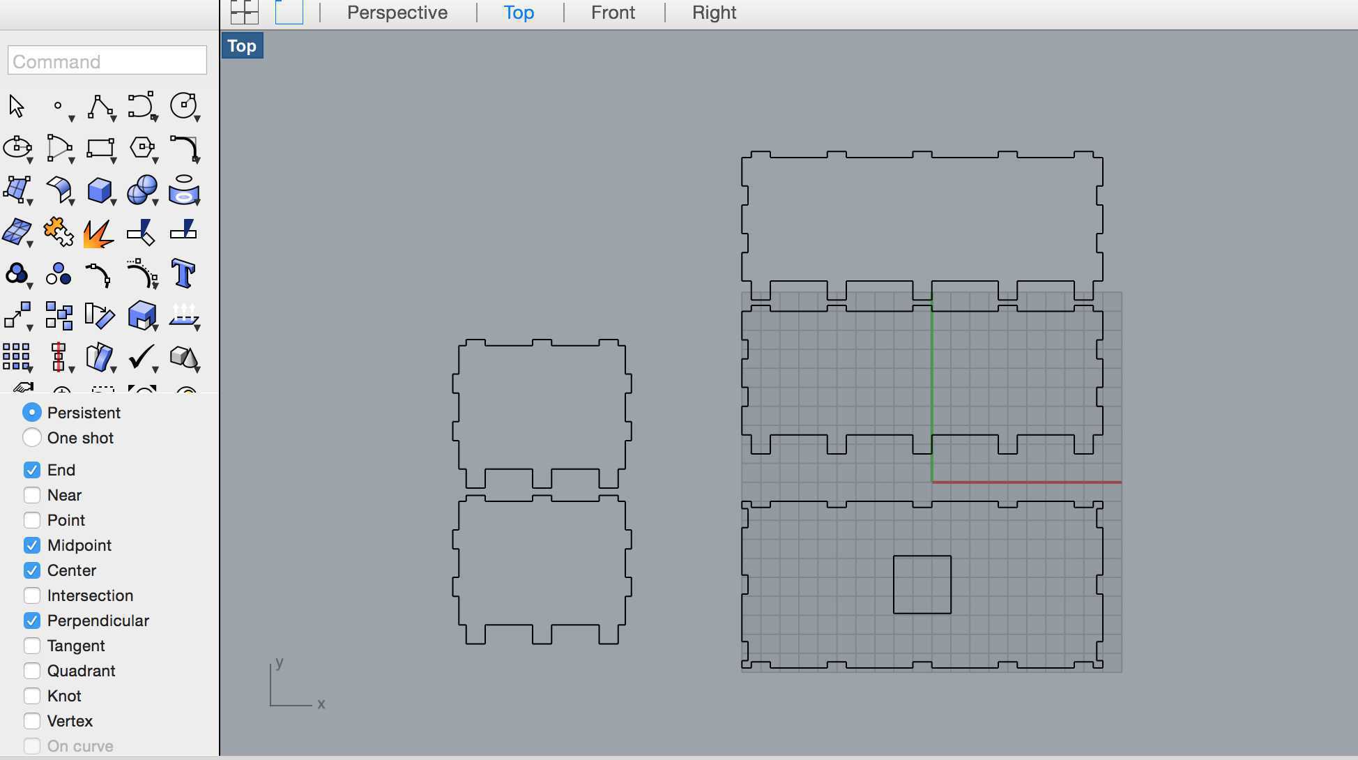
Figure 16. Final Rhino design of press-fit enclosure.
That should cover all of the physical apparatus parts! Now onto the final electronics designs.
Alright, remember, that the electronics part is just the construction of a photogate: a phototransistor connected to a microcontroller and a BlueTooth module, and an LED shining light through a cell culture tube. I am using a very bright LED, so I need it to be powered by a 9V battery, which will be connected to the LED by a 2x2 header.
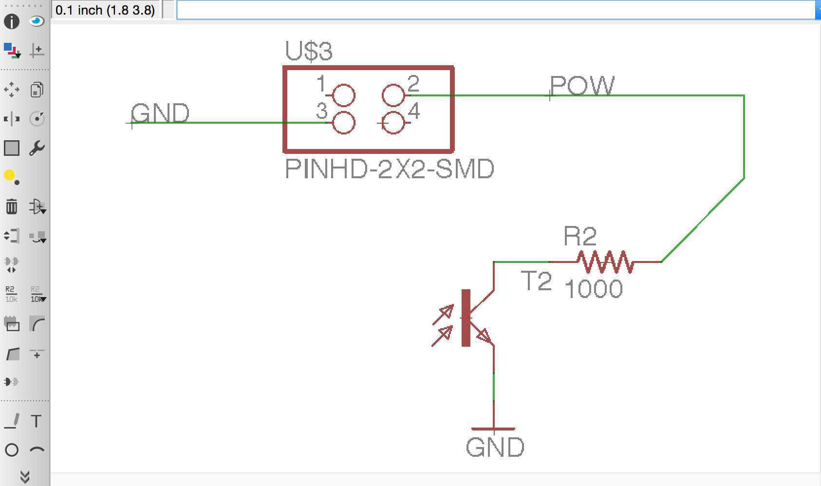
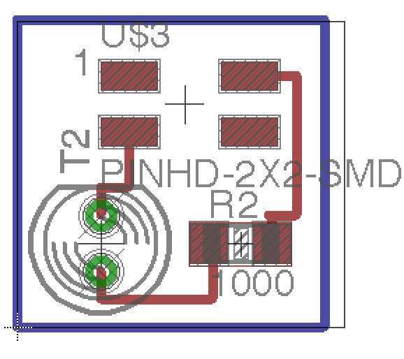
Figure 17. Final LED board design.
The phototransistor is a bit more complicated: I don't want more than one battery in the final product, so I will use a regulator to convert the 9V to 5V to power the microcontroller. Othe than that, I just need connections for the Bluetooth LE (TX and RX), and that should be enough to read the serial output from the device.
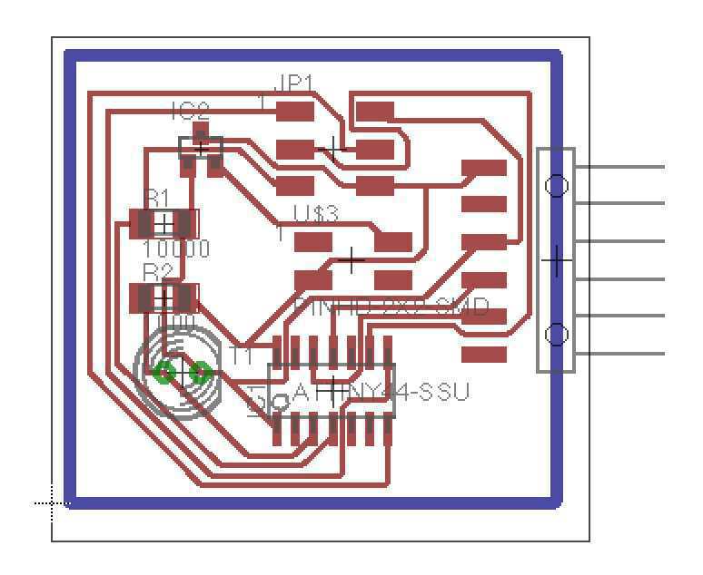
Figure 17. Final (probably not final) phototransistor board design.
Also, I figured out my milling error! I was sending the files by email and so the resolution got lost. Now, I just use DropBox, and the milling looks so much better. The stuffing and testing will happen soon!
Figure 18. Finally, a good mill!
Building the FabSpec
Constructing the Rest of the Physical Apparatus
Milling the Base
Alright, here we go! Time to build the FabSpec. The organizational strategy of the final project was to first build the physical apparatus and subsequently make the electronics, program the device, and have it communicate wirelessly. Of course, if all of this finishes, I can then make the device look nice and do cooler things.
My first goal was to build the base of the device. As you've seen previously, I molded and casted a small base, but realized that it would definitely not be big enough to hold all of the components, let alone the electronics. Thus, I decided to build an enclosure that would both house the electronics and internal components and also prevent light from entering the device so the LED won't have to compete with external ambient light.
It made sense to me to mold and cast the base. Yes, it was going to be big, but I found a gigantic wax block that Tom let me use. I set up the toolpath as you see in Figure 14, by specifying a ballpoint 0.125 end mill, which should pjust barely fit into the small press-fit holes. After loading it onto the ShopBot software, I zeroed the machine, and started it. The roughing toolpath went fine, but when it came to the finishing toolpath, the endmill broke once it tried to get into the crevice.
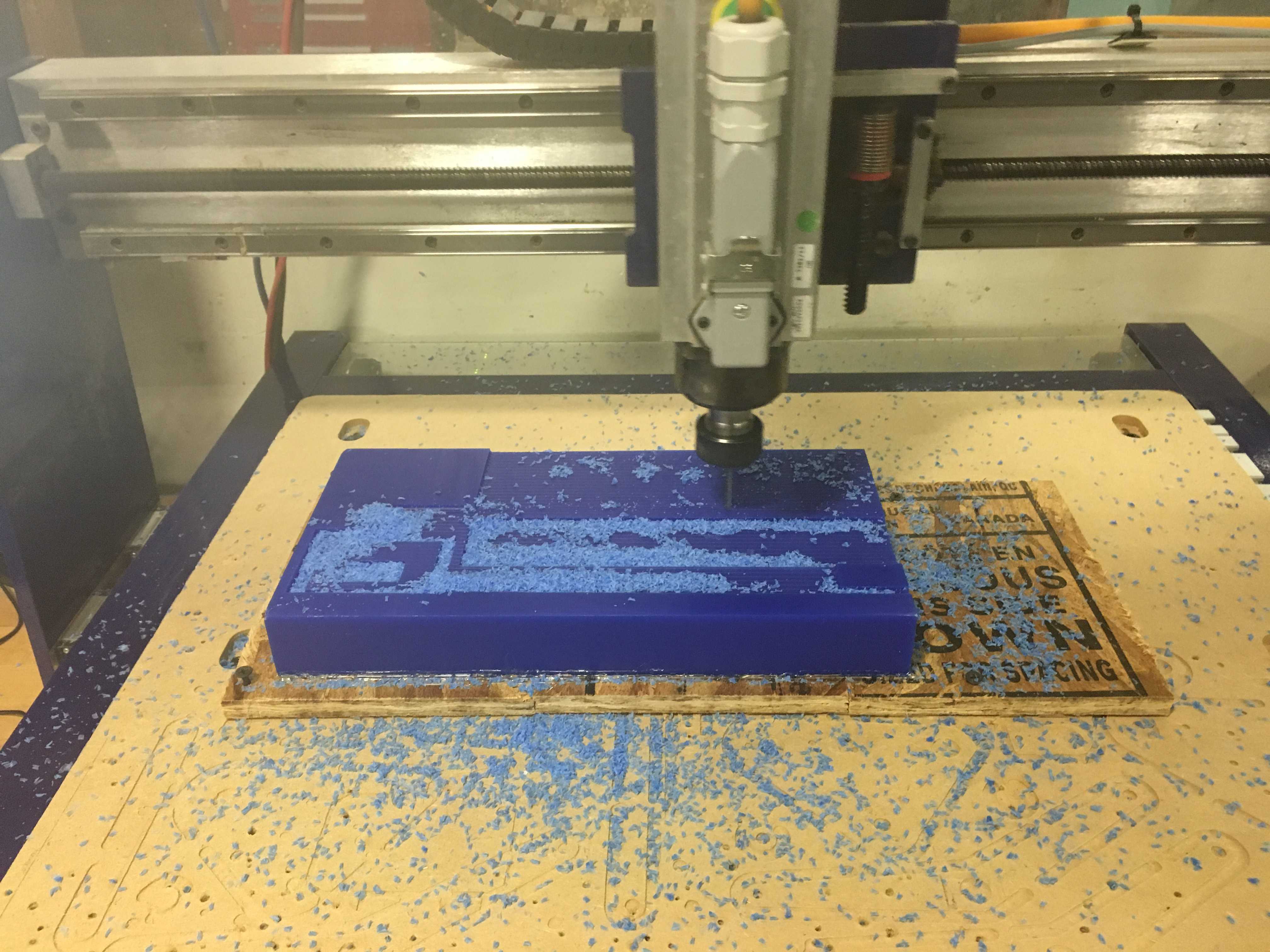
Figure 19. The 0.125 end-mill broke during the wax mill.
Tom and John were as confused as I was about why this happened. We thought it may have been my design, but ruled that out because I enlarged the holes by 0.01% using the gumball tool in Rhino to make the toolpath. Then, perhaps it was the endmill that was too short! In the end, I realized that this process was way too cumbersome for just a base, and the casting process could yield minor imperfections that could affect the final fit. Thus, I wanted to find an alternative. In comes TA Sam! Sam suggested that I still mill something, but instead of molding and casting it after, I just use it as the base. He suggested using HDP, a soft, millable plastic-type material that I can design in 2D like we did in computer-controlled machining week. The great thing was that it's black, which will achieve my goal of blocking ambient light from the bottom. Additionally, I used this opportunity to simplify my design, and put trenches instead of holes, to make the milling and fitting easier.
Figure 20. A simplified 2D model of the base to be milled with HDP.
To create the toolpath, I just used VCarve, and specified the outside to be milled in profile, while the inside to be pocketed at a depth of 10 mm. The entire processs of resetting this up and getting my base done was really quick!
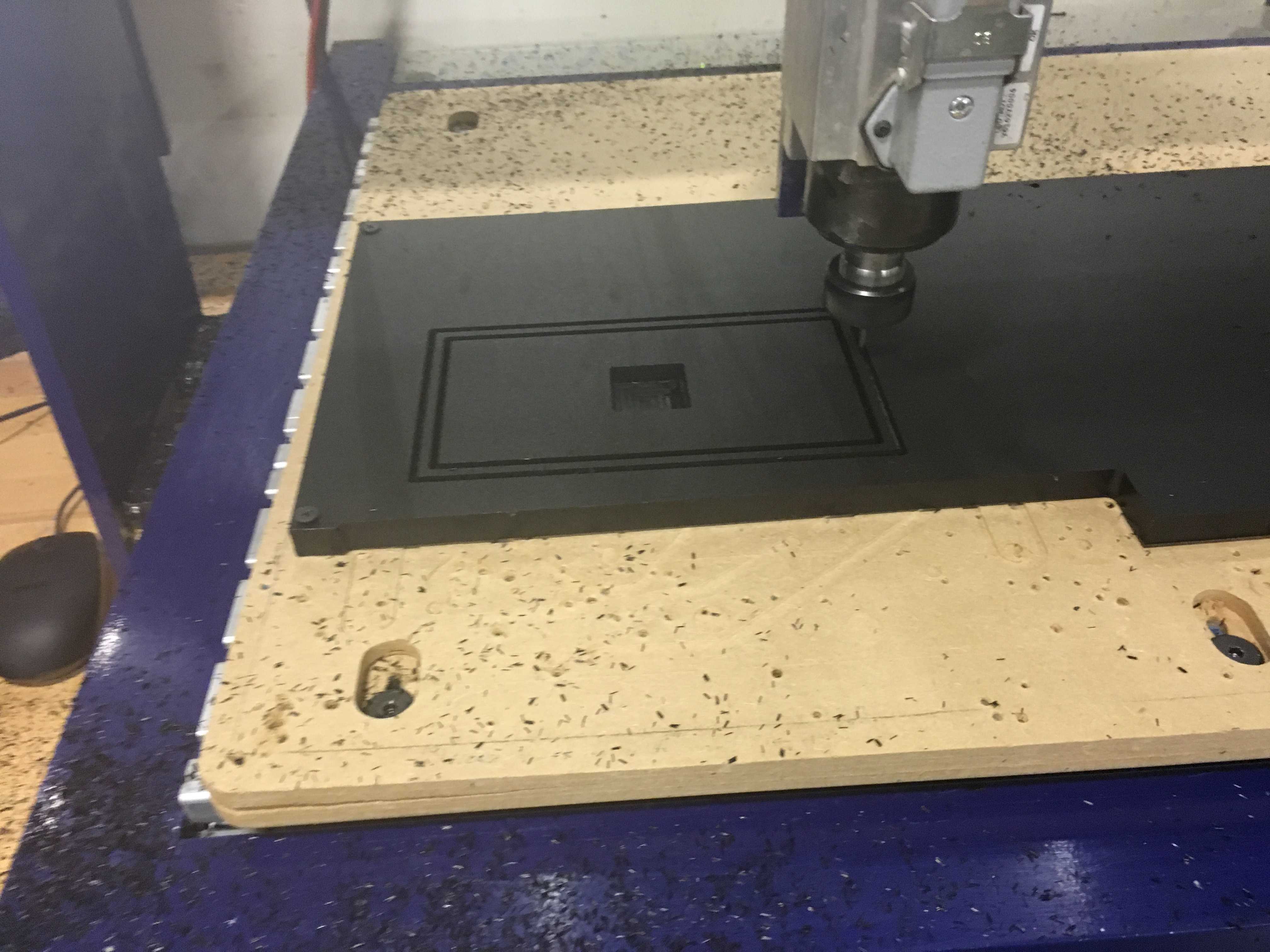
Figure 21. Milling the HDP base.
In the end, it came out excellently and fit the tubeholder perfectly!
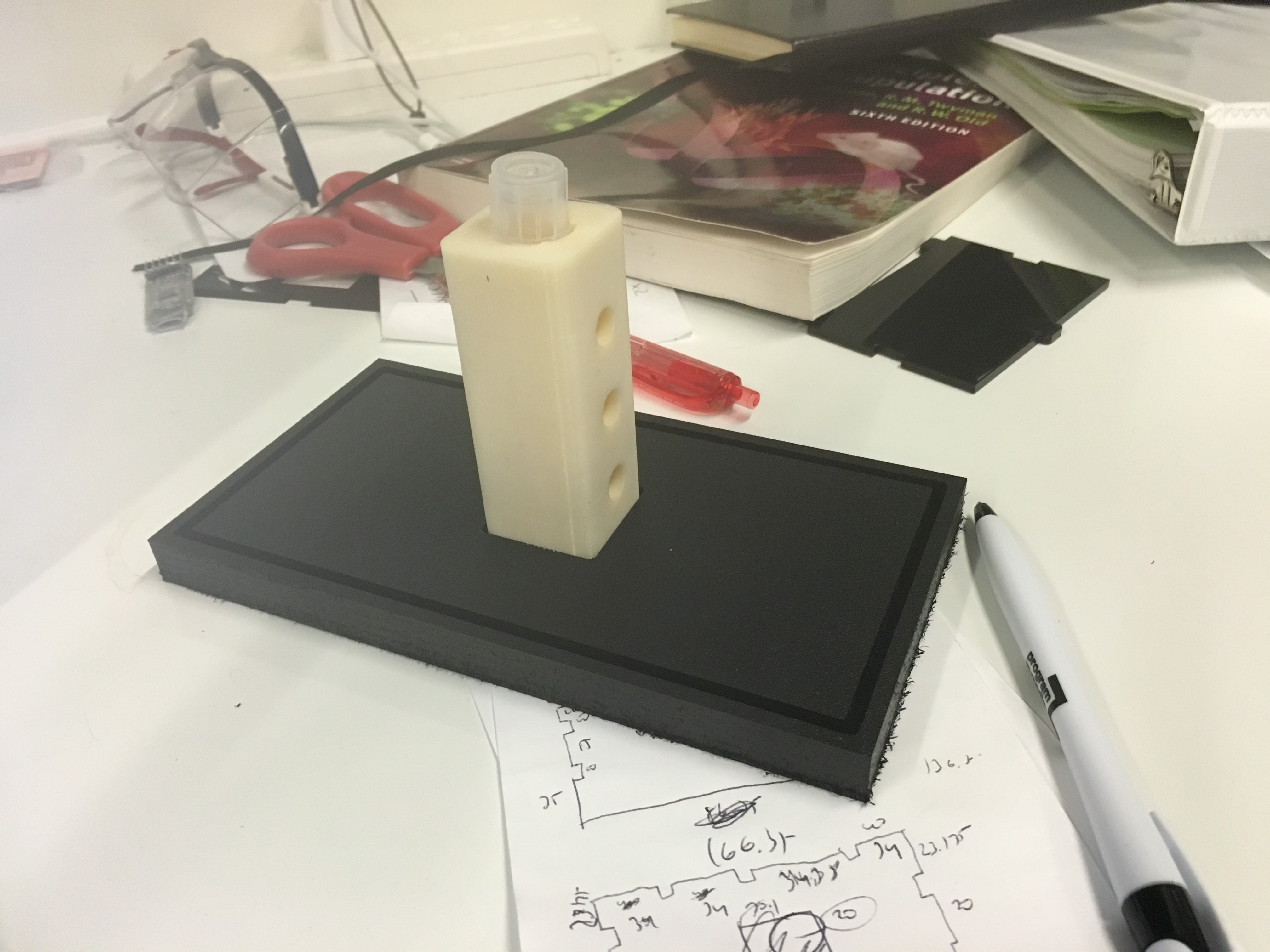
Figure 22. The final base! It looks awesome and fits great.
Laser Cutting the Enclosure
With the base milled, I just had to simply design a press-fit enclosure. To keep the light out of the interal part of the device, I settled on using 0.125 inch Delrin as a strong, laser-cuttable material that would fit together nicely in the 0.125 inch wide trenches. My Rhino design also included a top that would allow for the insertion of a tube into the tube holder, letting minimal light in.
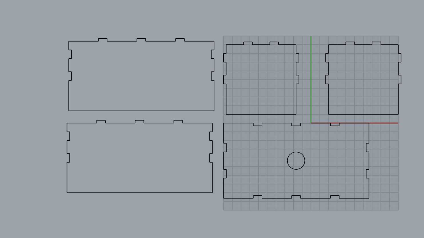
Figure 23. The final Rhino design of the press-fit enclosure. Note that the bottoms of the sides are flat to fit into the trenches, and the top has press-fits for the side parts and a hole to allow for insertion of the tube.
Since I wanted to finish the laser cutting soon and move on to the electronics and it was late at night, I decided to use the Trotec laser cuttter in the CBA lab E15-023. I hadn't done it in a while, and thankfully, Ben, a CBA graduate student and the owner of Yoko, was there to help me cut my parts. Because it is a small laser cutter and pretty weak, I had to do >7 passes, just to get the pieces out.
Figure 24. Laser cutting the enclosure. It took >7 passes to cut through the Delrin.
In the end, the pieces came out beatifully, and fit perfectly in the base and around the tube holder to create the final physical apparatus!
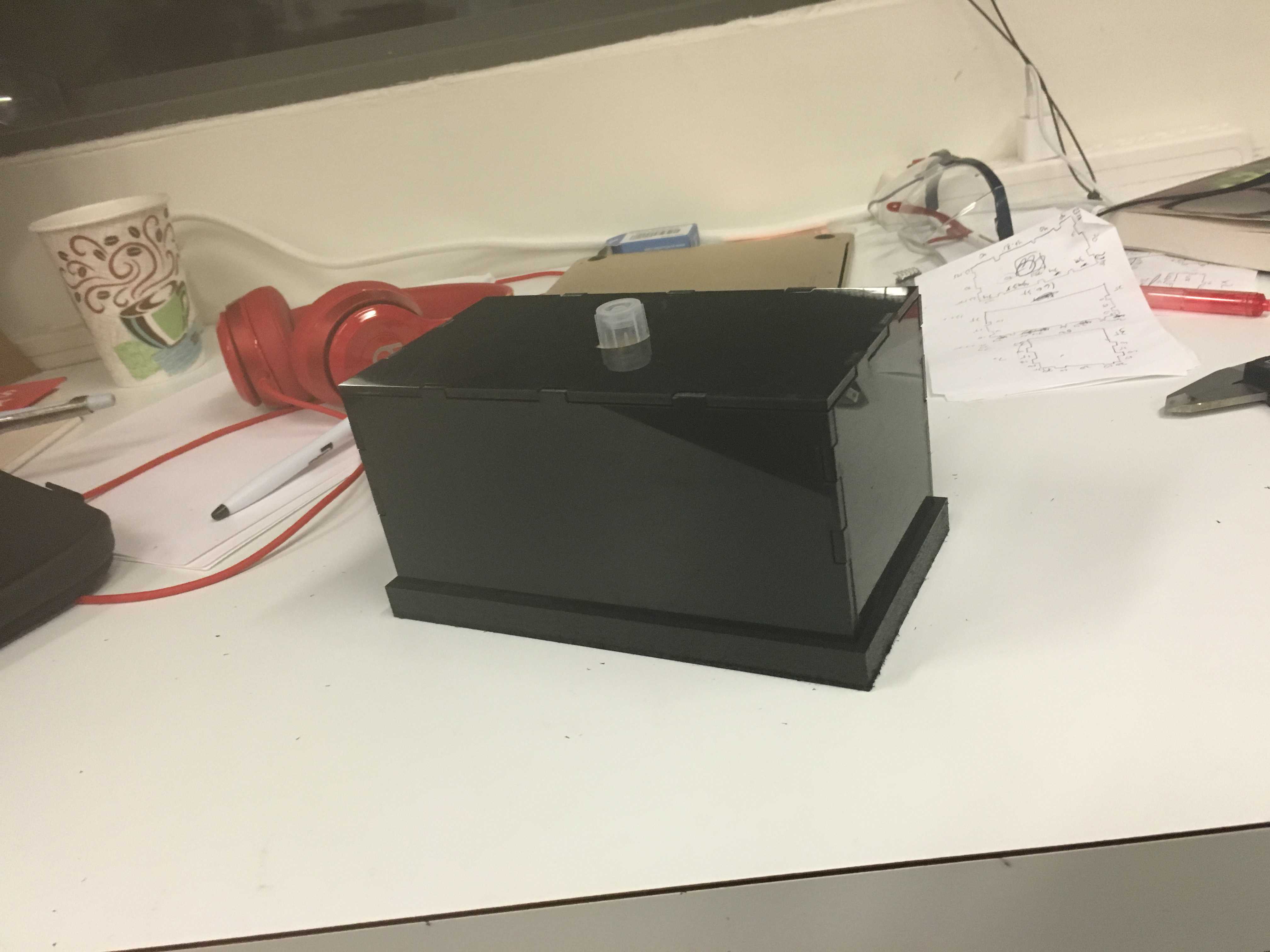
Figure 25. The final physical apparatus is built and looking great!
Electronics and Communications
Now onto the grueling part of the execution phase: making the electronics work. As you can see over the past few weeks, I have gone through countless designs, trying to nail the perfect one for the the photogate. It comes to no surprise that I still had to continue editing the designs.
The LED Board
This board was super simple. Looking above, you can see that I just have a 2x2 header, which will connect to a 9V battery and power a bright white LED through a 1k resistor. I later realized that I didn't need the resistor since the LED had built-in resistors, so I just removed it and designed an uber-simple LED board, connecting the 2x2 header to the LED.
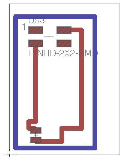
Figure 26. Redesigned LED Board!
The milling and soldering were easy, and the LED shined brightly when connected to the 9V battery.
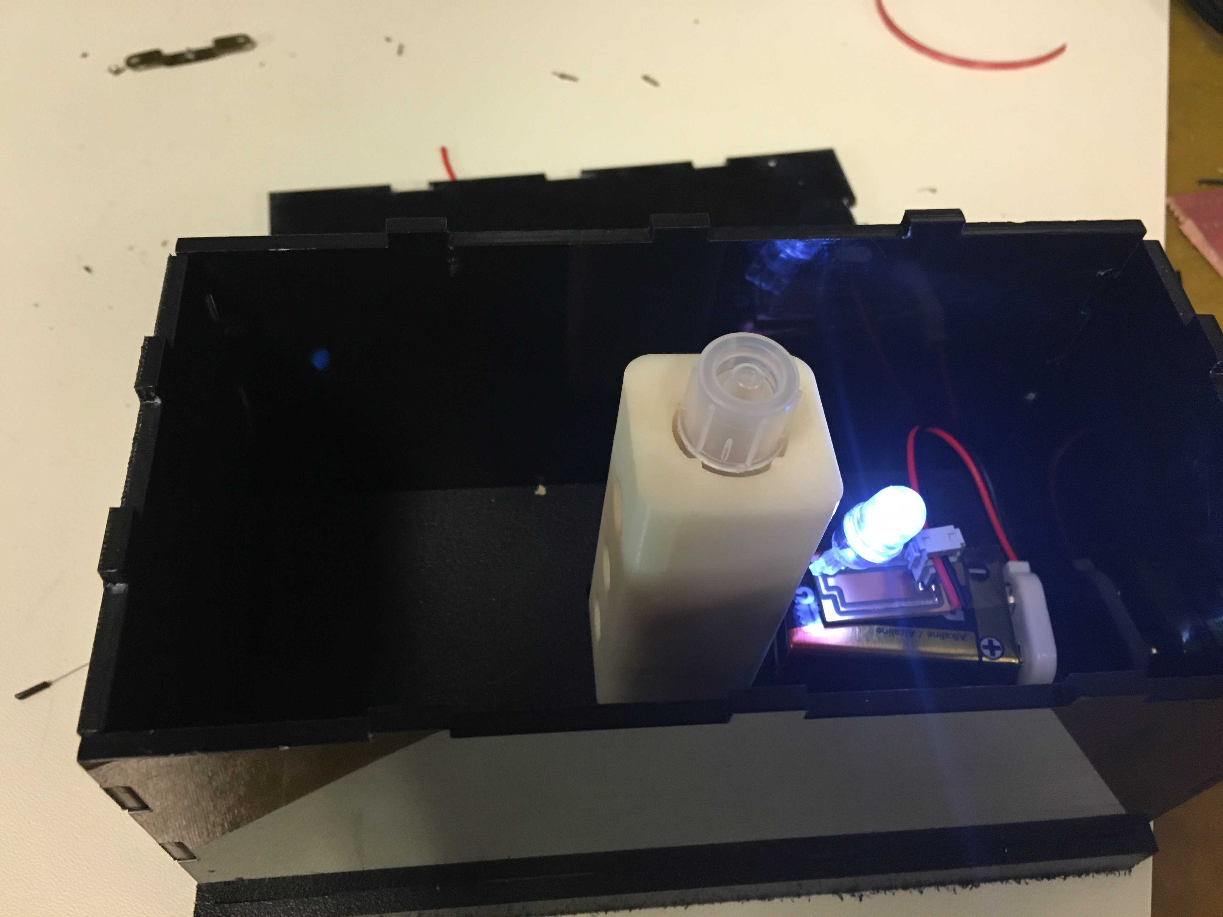
Figure 27. Constructed LED Board in the apparatus!
The Phototransistor Board
This was going to be the hard part. I went through so many designs and iterations, and I kept on catching more mistakes. First, it was that I didn't connect properly to the phototransistor. Then, I realized that I was using an IR phototransistor, that would read light at the wrong wavelengths. I milled and stuffed a ton of boards, but there was always something wrong with it. Once, I didn't have my reset pin fully connected and then a trace just got torn off of the board. Another time, I had my phototransistor connected to a digital pin, when in fact, it should have been connected to an analog pin so I can do an analogRead for the values. Eventually, I fixed all of these problems, but not before going through many failed boards.
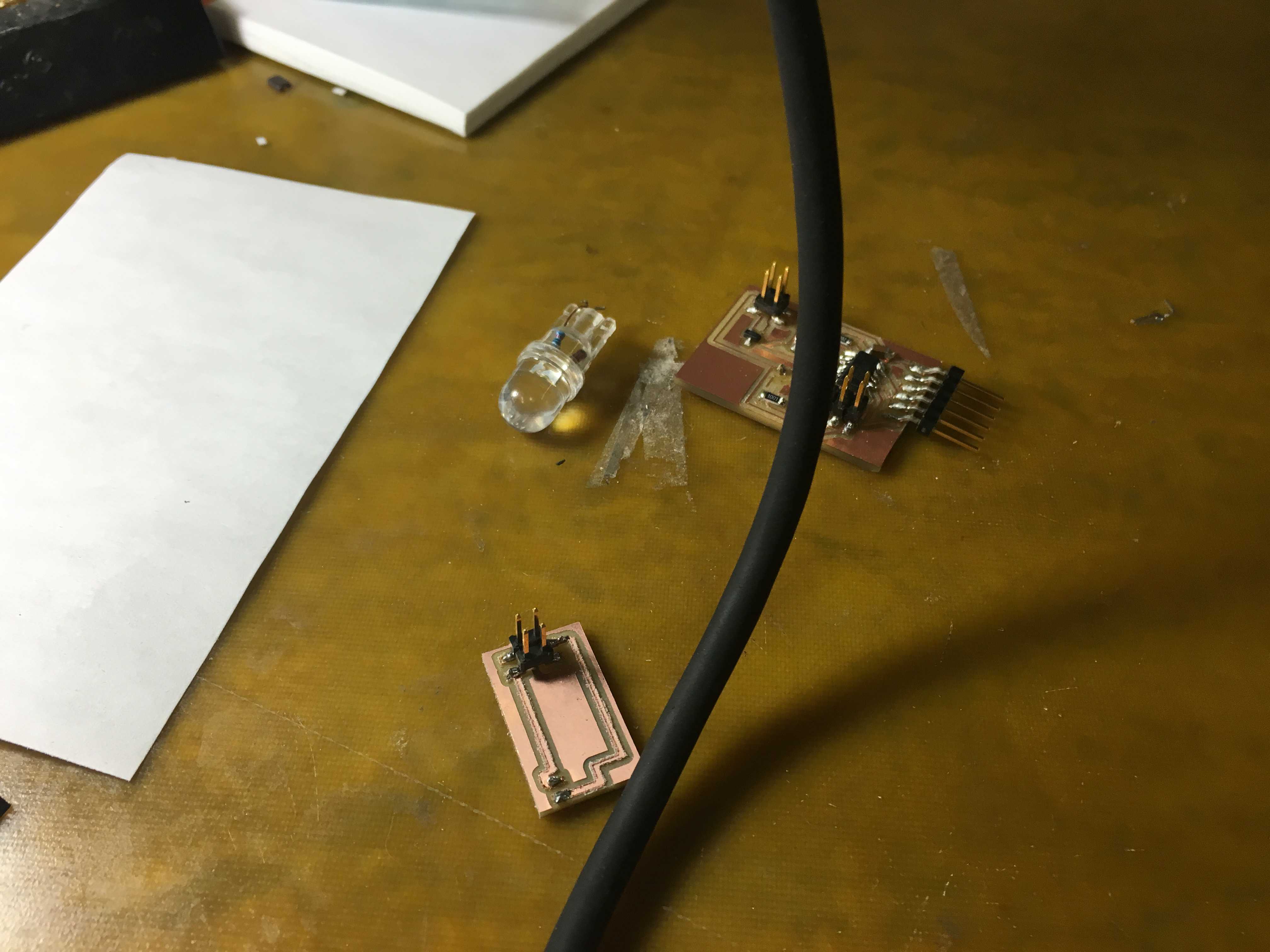
Figure 28. Many, many failed boards like the ones here!
Finally, I figured out all of the problems, and converged on the perfect design. Overall, the design idea is similar as the ones explained earlier: use an ATTiny44 as the microcontroller, connect Pin 2 to the phototransistor, have RX and TX connected for wireless communication, have a 3.3 V regulator connecting to the 2x2 header to the 9V batter, which will power both the microcontroller and the BLE, and a 3x2 header for programming the board, appropriately connected to the ATTiny44.
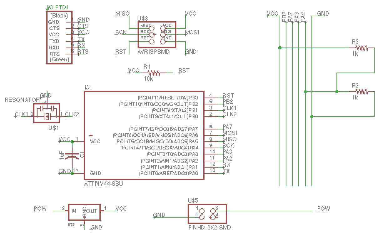
Figure 29. Final schematic of the phototransistor board.
After arranging the board to look like the initial HelloWorld board, I autorouted the traces according to the design rules, and I got one 100% routed design, which looked clean and friendly.
.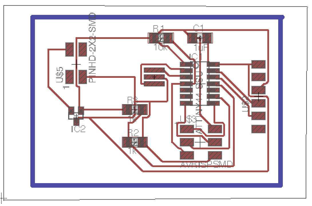
Figure 30. Final board design of the phototransistor board.
After milling and soldering the board, I got power running through the board successfully!
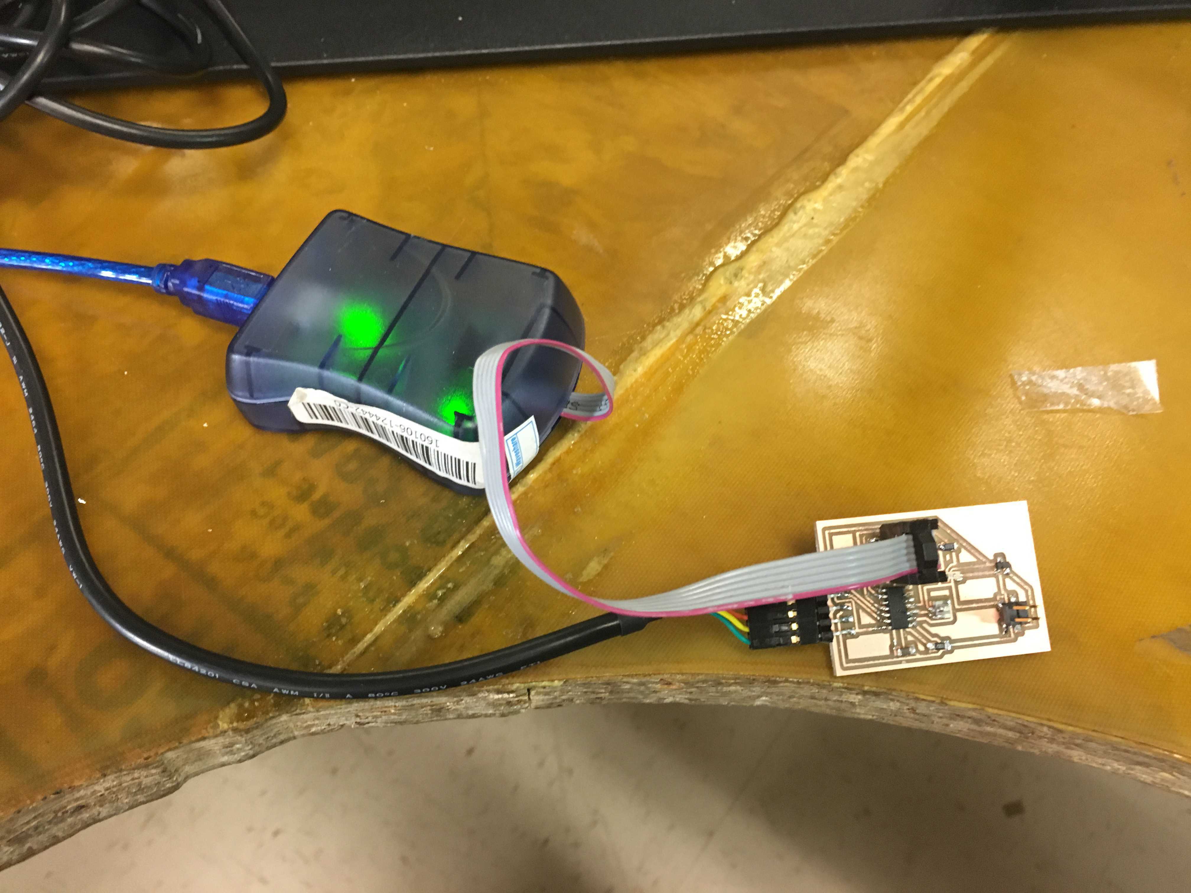
Figure 31. Power running through the board.
Nonetheless, I still had immense trouble burning the bootloader. In fact, the ATTiny44 even began to heat up when powered, so I was really nervous. But thankfully, I figured out what the problem was: the Reset pin was not fully soldered, and MOSI pin was also disconnected, not allowing for the AVRISP mkII programmer to connect with the microcontroller. Once I fixed these connections, the bootloader burned perfectly.
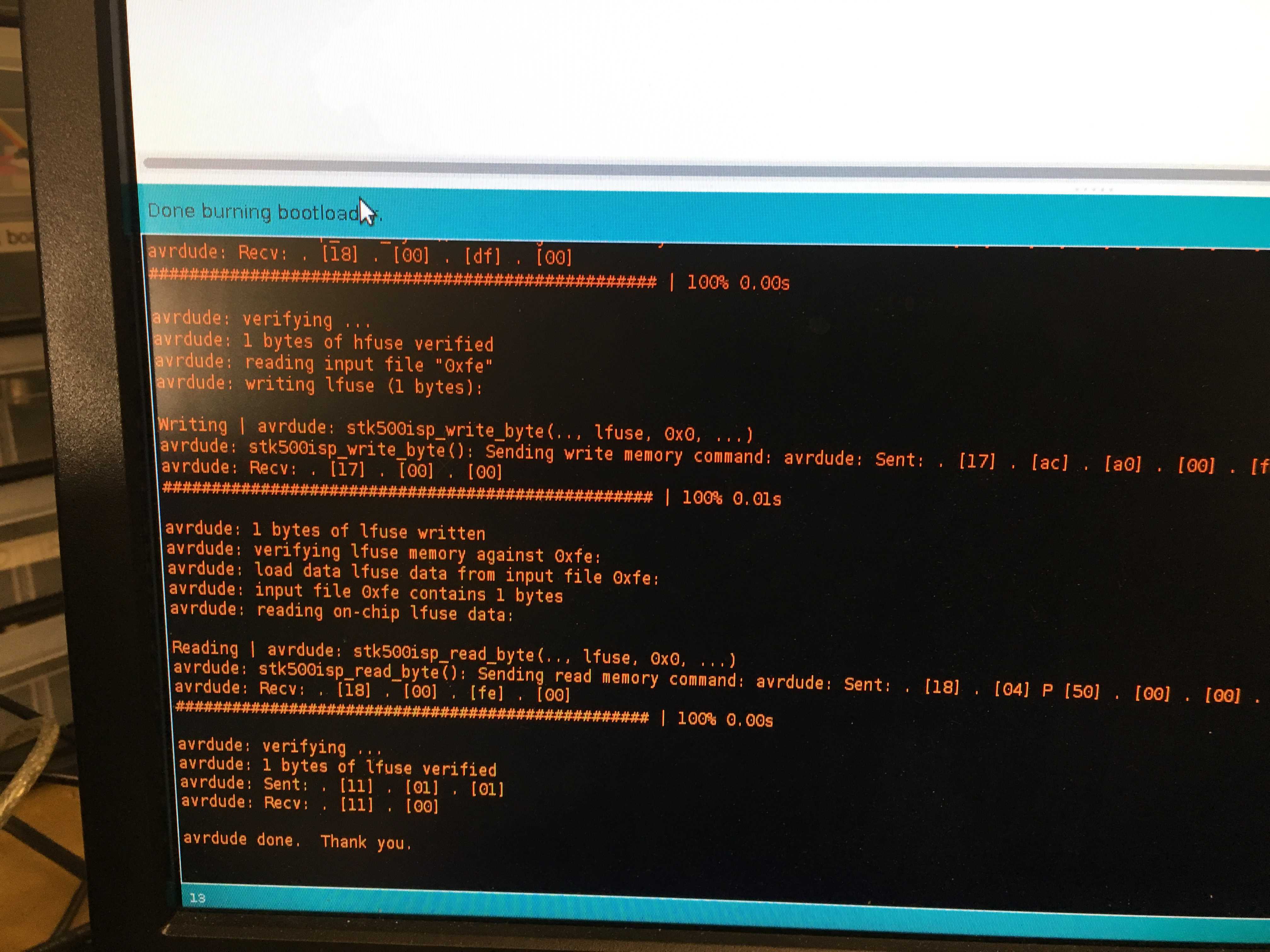
Figure 32. Burning the bootloader: check.
Everything was really smooth from here. I wrote a short script that would print out the analogRead from the phototransistor (and eventually to the BLE interface), and it verified and uploaded very easily.
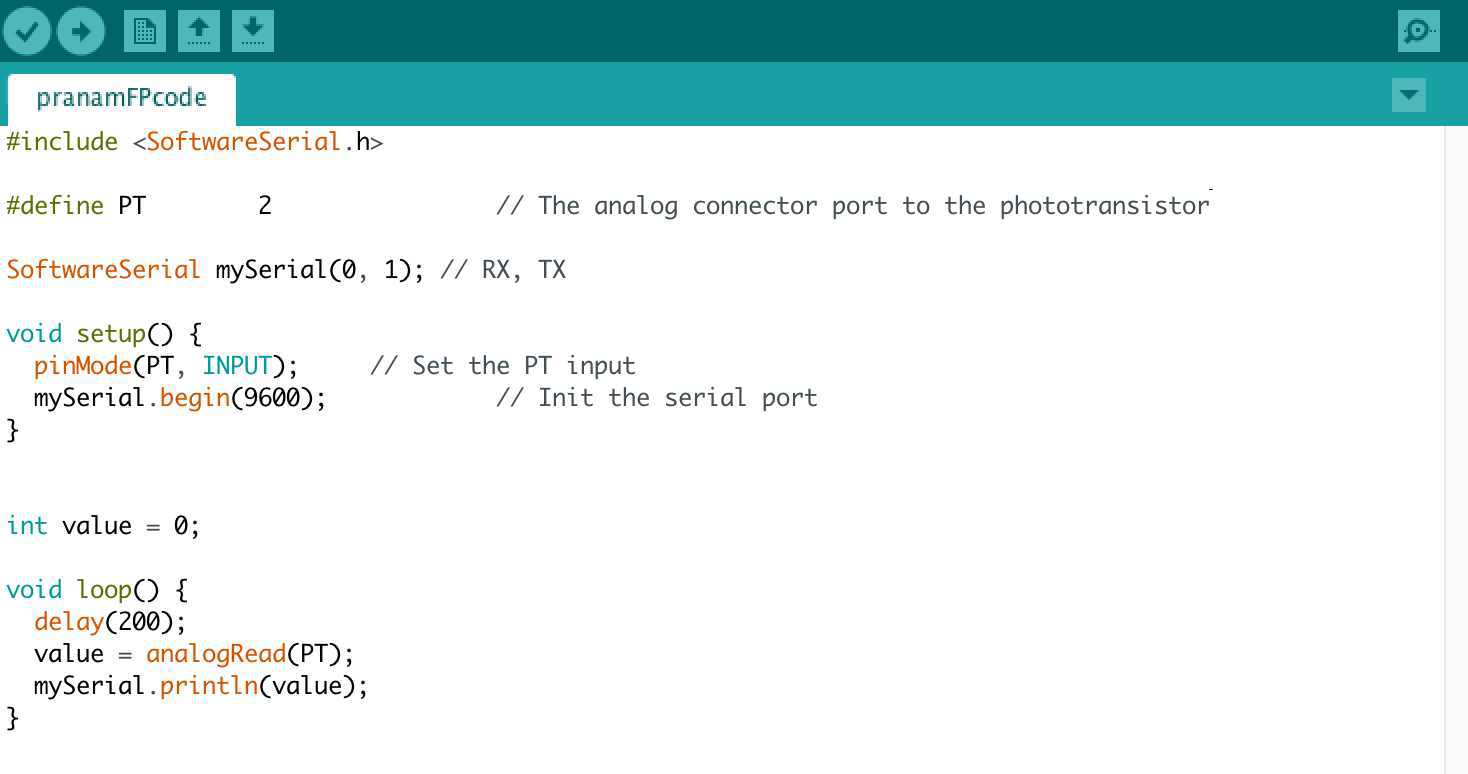
Figure 33. Arduino code reading the analog signal from the phototransistor with a short delay.
Bluetooth LE Communication
Now that the board was programmed and communication serially, it was time to interface with the BLE, something I wasn't able to do during Week 12. To do this, the first task was to connect the BLE to power, which had to be done by connecting VCC and ground, and connecting the RX pins to TX and vice versa. I worked closely with Shani as well followed Yasmine Rubinovitz's (a 2015 student) tutorial on BLE communication. And as expected, the BLE HM-10 module blinked when it received power, since 3.3 V was powering it through the regulator!
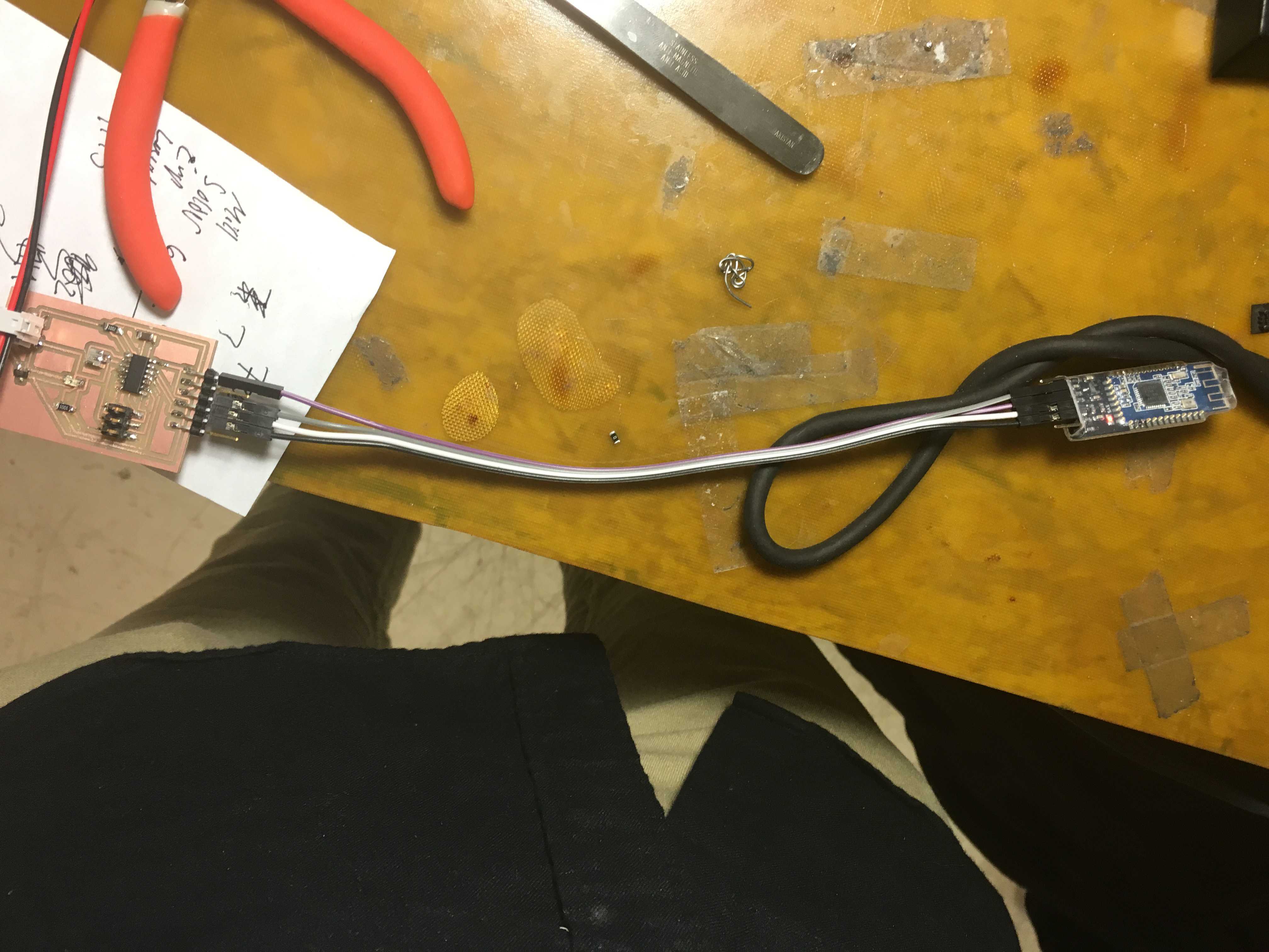
Figure 34. The HM-10 module receiving 3.3 V of power and blinking.
Next, I opened LightBlue Explorer on my phone, and I connected to my device named HMSoft,which can be found on the Serial Monitor on the Arduino IDE using AT commands. Check out the How To Make Bluetooth tutorial on AT commands.
.
Figure 35. Connected to the HM-10 on my iPhone.
Now that the communication was good, I could receive the analogReads from the phototransistor board, which was connected to the BLE module! I converted the read messages from HEX to Strings, and VOILA, the board read higher and higher values as the phototransistor was exposed to light! SO COOL!
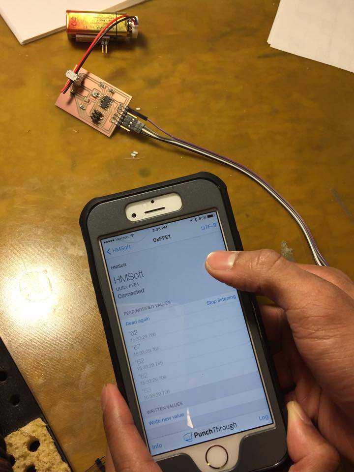
Figure 36. Receiving phototransistor values on my iPhone!
With the BLE connection working and reading the board, it was time to improve the reads it got from the phototransistor. Unfortunately, the phototransistor board does not fit well around the tubeholder, which has holes specifically for the LED and phototransistor. There was no way to mount the board to get clean reads from the LED through the tube. With Grace's suggestion, I decided to make a breakout board that would just connect to the phototransistor. This board would be directly attached to the hole on the tubeholder so not only would the phototransistor be directly across from the LED and tube, but also would be blocked from receiving any other light, if any light happened to creep in. To do this, I used male-to-male cables, clipped off a part of the headers, removed the phototransistor from the board, and connected the cables through holes, to the new board (design shown below), and attached to the pads on the main board.
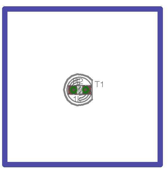
Figure 37. Breakout board design. The green circles are milled as holes to allow the wires to go through.
After milling and soldering this simple board and making the connection, I attached it to the side of the tubeholder and placed all of the components inside the physical apparatus. I used double-sided tape as an adhesive, and even used the casted old base as a stage for the LED board! In total, the inside looks pretty messy, but the outside looks really snazzy when the top is put on, as shown in Figure 25.
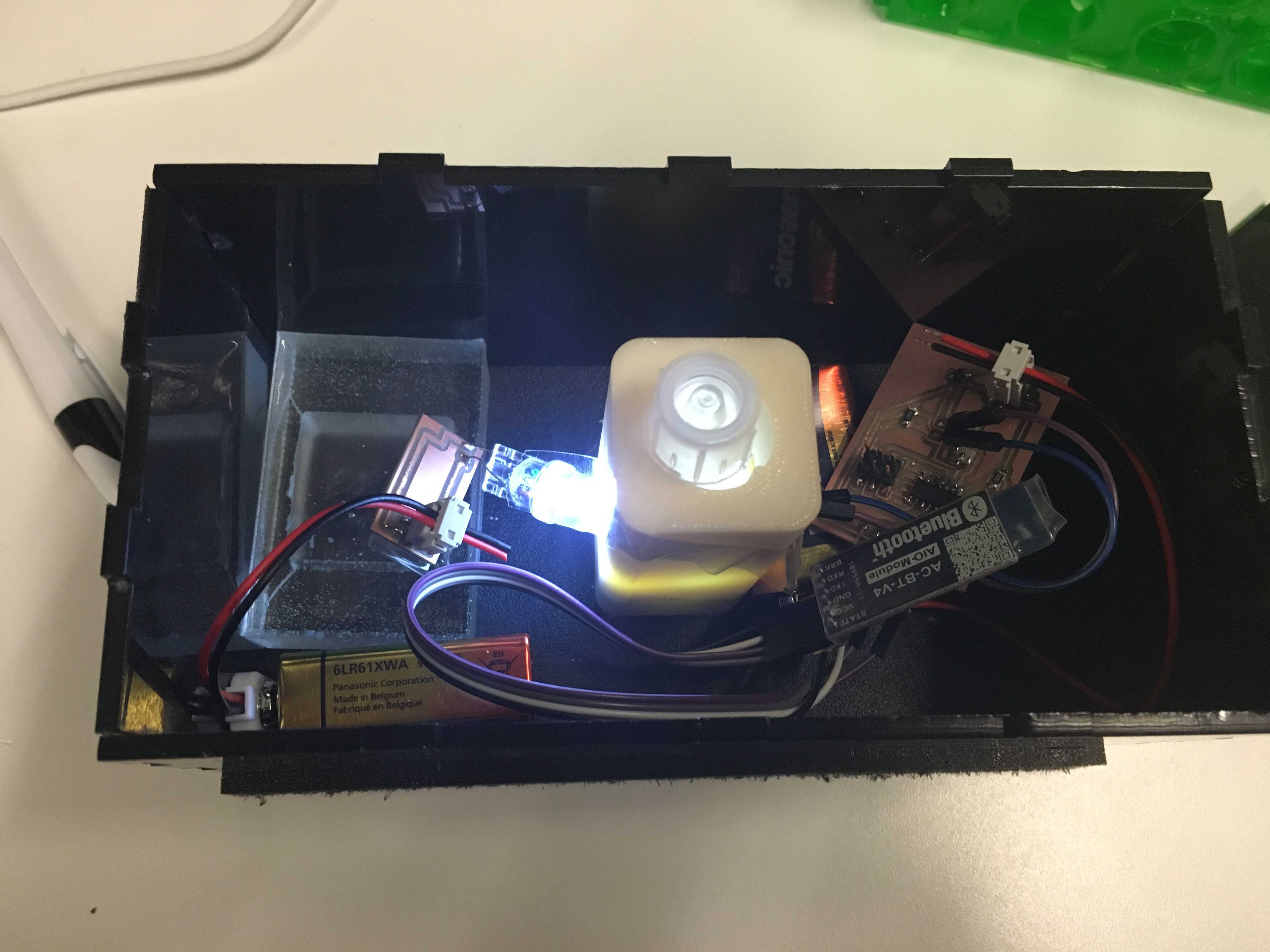
Figure 38. The internal components fit inside the physical apparatus. The FabSpec is coming together!
Calibrating and Testing the FabSpec
Calibration time! It was time to run some actual samples to make sense of the values read on the BLE app, and determine appopriate threshold values. I filled up one tube with just growth media, and one with a sufficiently grown bacterial culture.
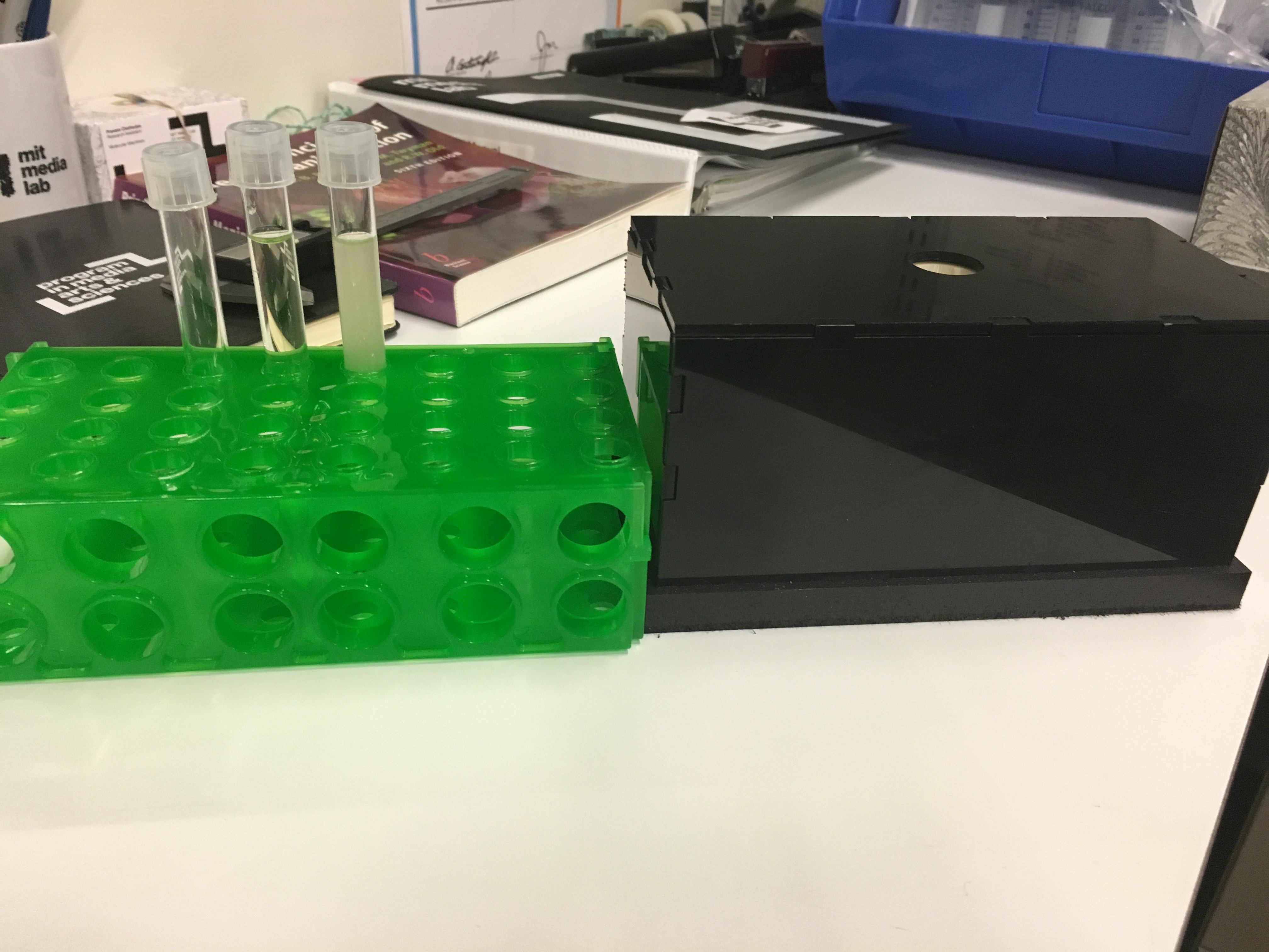
Figure 39. Three conditions to test for calibration purposes (from left to right): empty tube, tube with culture media, tube with fully-grown bacterial culture in same growth media.
I inserted the tubes and read the values from my iPhone! First, the empty tube to measure baseline values.

Figure 40. Phototransistor values for empty tube. Average value = 7.8.
Next, the "blank" sample: the tube with clear growth media.

Figure 41. Phototransistor values for media tube. Average value = 18.2.
Finally, the experimental sample: the tube with a sufficiently-grown bacterial culture. This will give us the value that we can set to be the threshold.
.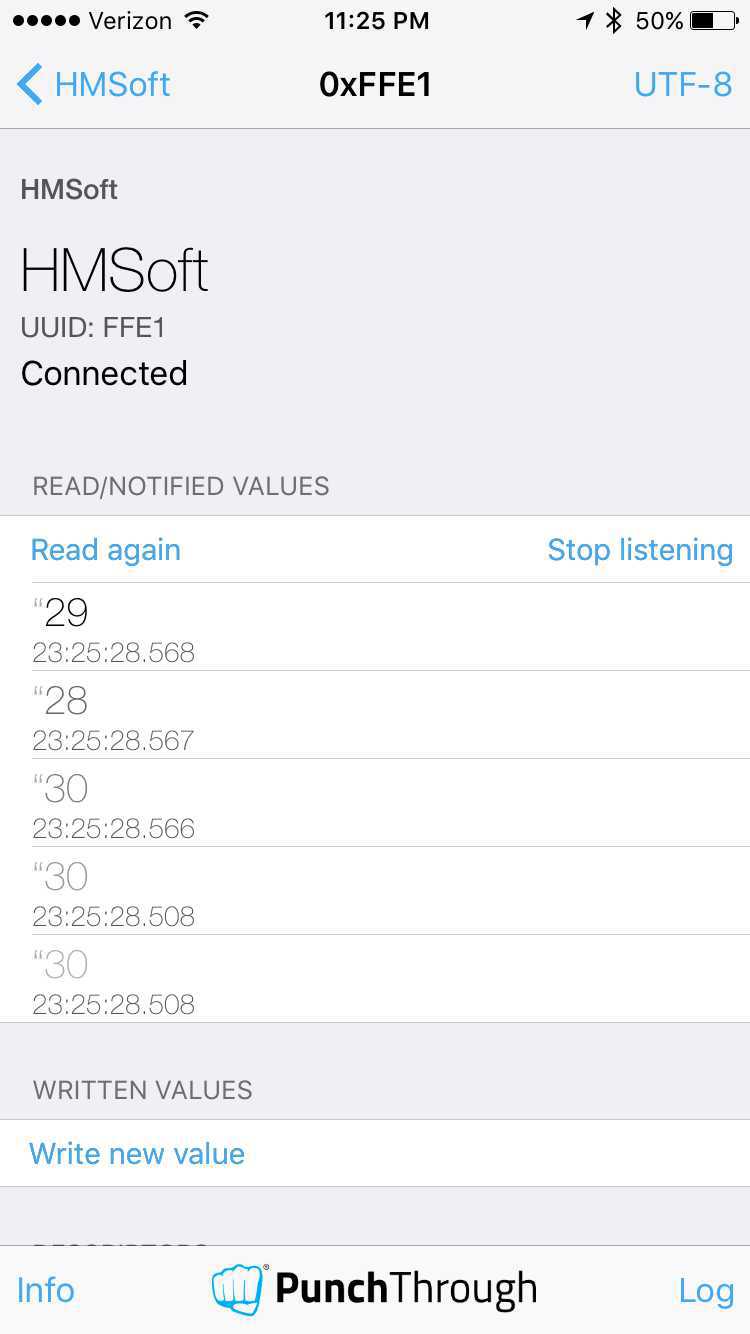
Figure 42. Phototransistor values for bacterial culture tube. Average value = 29.4.
As you can see, the values are very distinct for the three conditions. A threshold value of 28 is sufficient to separate cultures ready for DNA extraction and those that are not. This simple experiment validates the successful construction of the FabSpec!
An Attempt at Building an iPhone App
I really wanted to build an interface for the FabSpec, and since I was receiving Bluetooth data from my BLE module, if could write a quick iPhone app to read out the data and send a notification when the bacteria is ready, it would be a great addition to the project. I again took hint from Yasmine's page and downloaded Ionic, where I could have a starting framework to build an iPhone app. After downloading a blank project, I git cloned an Ionic BLE repo from Github, and modified the code in the index.html file from the www folder to read the values from the phototransistor and return a simple string to indicate that the bacteria is ready to harvest. Unfortunately, I realized halfway that I could not deploy the app to my phone where the data would be read, because I am not an Apple developer, and using the simulator in XCode would not allow me to access the data being read solely to my phone. Oh well! I think a better option is to simply work within LightBlue Explorer and get a simple message read as data is sent to indicate when the culture is ready.
Improving Calibration and Simplifying BLE Message
As you know, I already had the values corresponding to different states, one sufficiently grown and a blank, so I decided to alter the C program so that the BLE would write a message to the LightBlue Explorer app, telling me (or any random molecular biologist) if the bacteria in the tube is "READY" for DNA extraction or not. I tested many different values around the range of 26-34, to see which value would give me no indication with an empty tube and a "READY" message with a dense culture tube. To do this, I just kept the programmmer plugged into the 3x2 header, with everything still attached (including power) so I could check values immediately, making the testing phase very seamless (many thanks to Ryan for his assistance during this process). Eventually, an OD measurement of 32 was a good threshold value to differentiate the two states! In the future, I will optimize this value based on the internal design of the FabSpec.
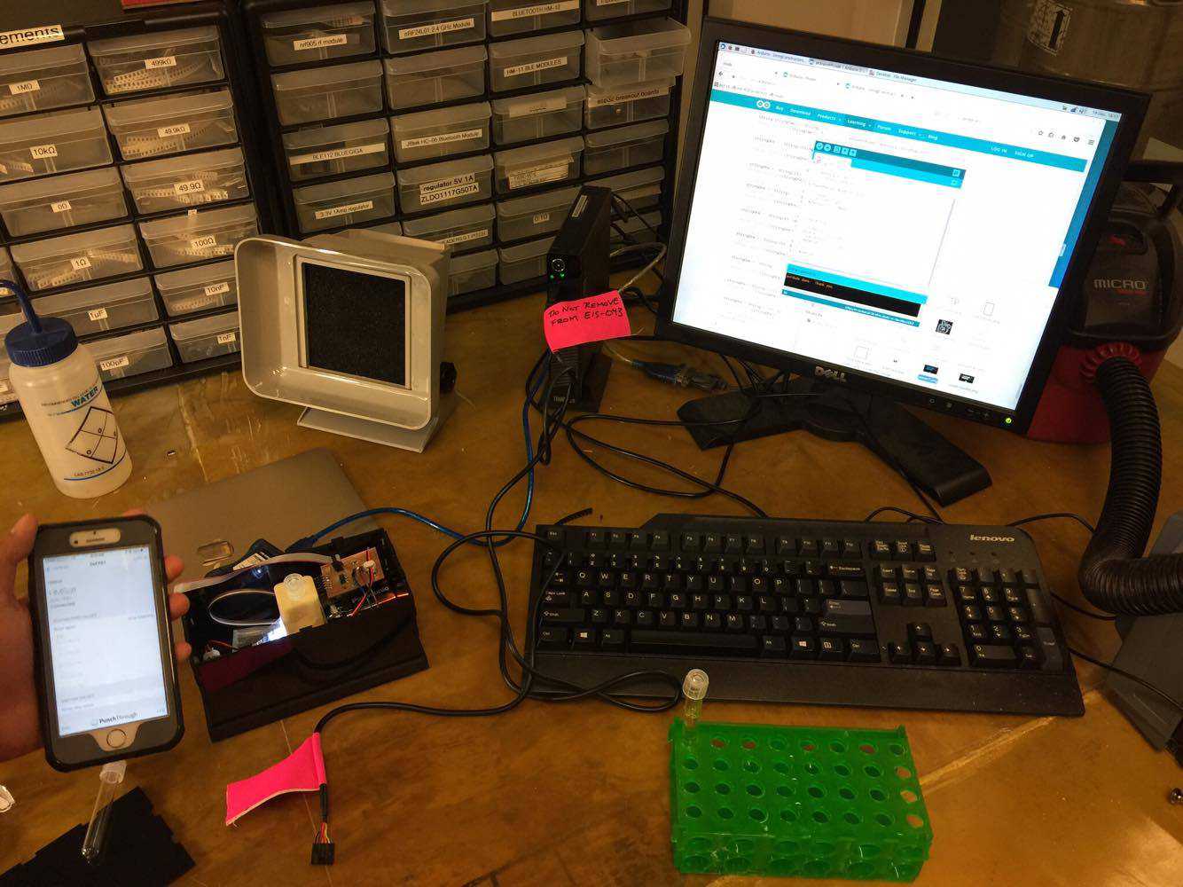
Figure 44. Rapid testing, calibration, and reprogramming of the FabSpec.
Adding the Finishing Touch
Now that all of the technical work is done, time to personalize the FabSpec! With a nice, sleek black box, a crisp white logo would work perfectly! And what's the best way to add a logo in How To Make? You guessed it: Vinyl Cutting! Nikhita carried me through the process as I somewhat forgot how to use the Roland machine, and I then used transfer paper to perfectly stick the logo onto the wall of the device!
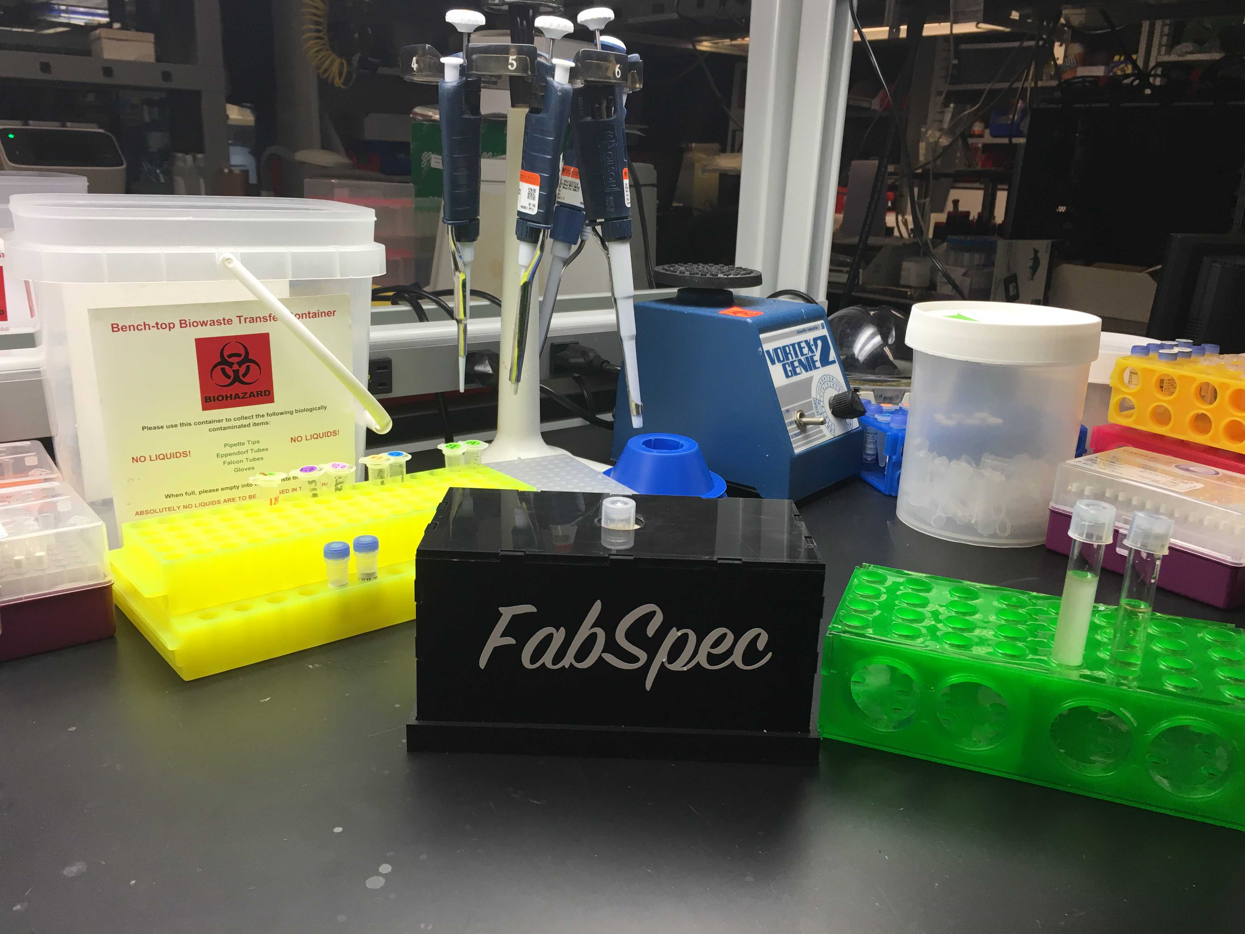
Figure 45. The final FabSpec deviec.
And there you have it folks: the FabSpec! Now, molecular biologists have a cost-effective, easy-to-use tool to add to their arsenal when assembling DNA constructs. With direct notifications to their phones, no longer will there be the need to do regular, manual measurements, so to allow for greater flexibility in doing research!
I want to extend many thanks to the staff and fellow students for making this semester of How To Make (almost) Anything absolutely amazing -- I had a wonderful time and learned so much! I look forward to continue using these tools and skillsets for future hacking and making purposes, both in my research and in life! :D
| FabSpec Component | Applied Modules |
|---|---|
| Tubeholder | 3D Printing |
| Initial Base/LED Stage | Molding and Casting |
| Final Base | Computer-Controlled Machining |
| Enclosure | Laser Cutting |
| LED Board | Output Devices, Electronics Design, Electronics Production |
| Phototransistor Board | Input Devices, Electronics Design, Electronics Production, Embedded Programming |
| Integrated HM-10 BLE | Networking and Communications, Interface Programming |
| Logo | Vinyl Cutting |