Characterizing Design Rules
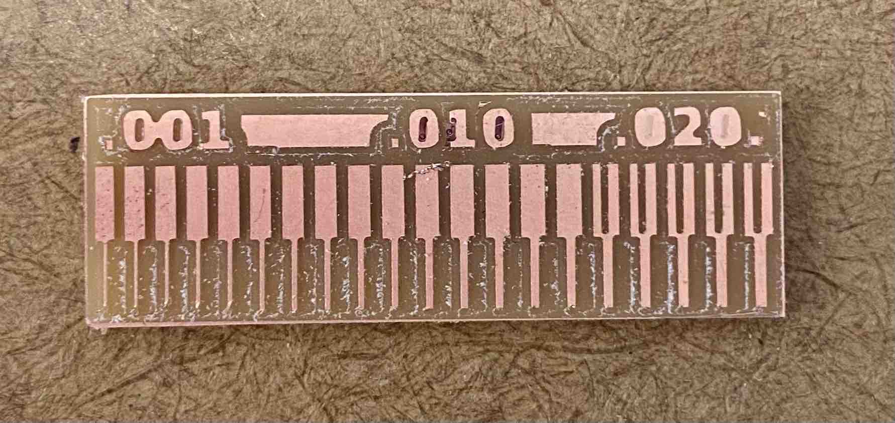
Here is the second version of the trace-width-testing PCB (the first one was gobbled up by the vacuum when I too eagerly jumped to cleaning the board after it had finished milling). The offset was 4, so the line quality is not so crisp.
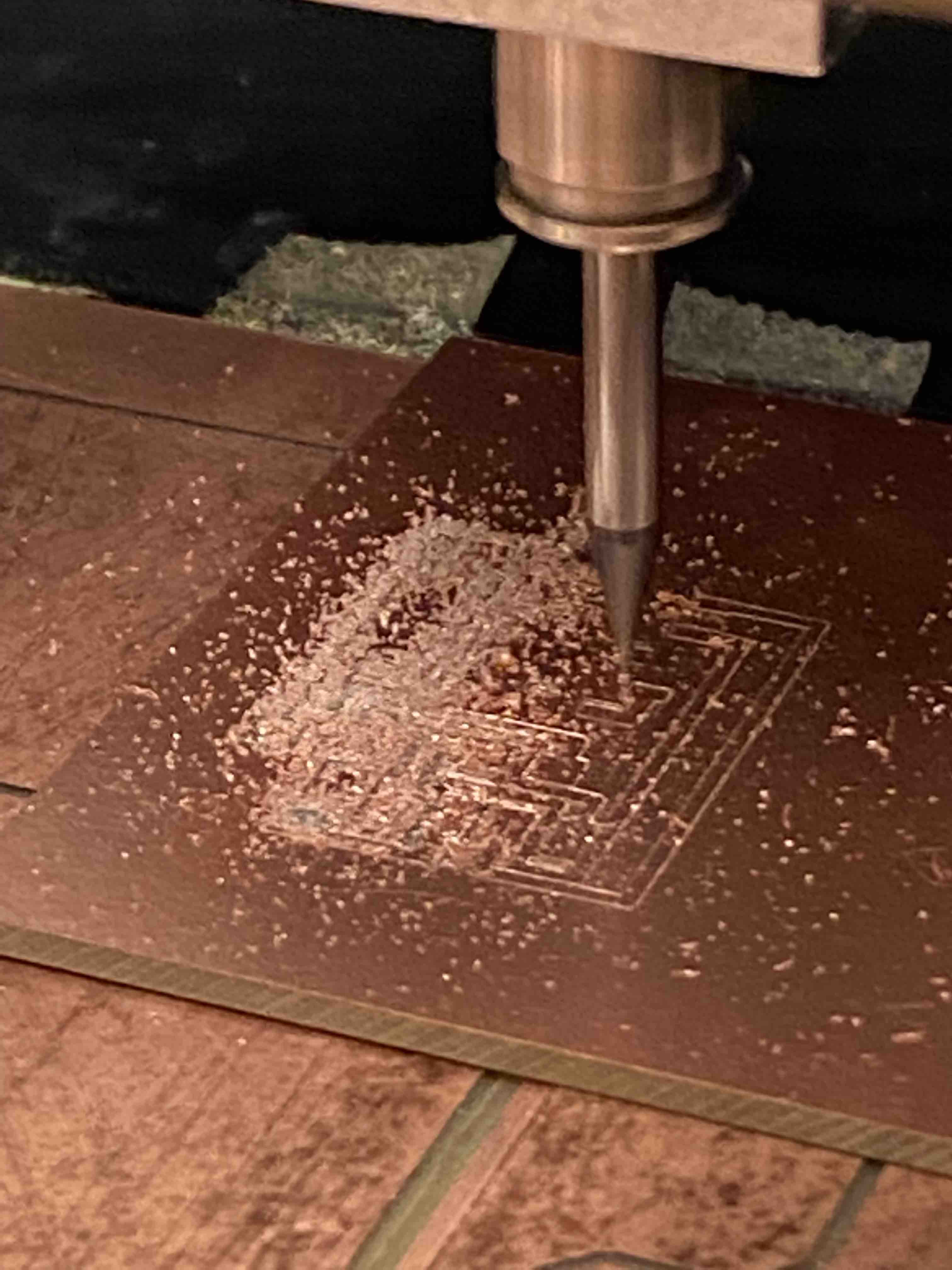
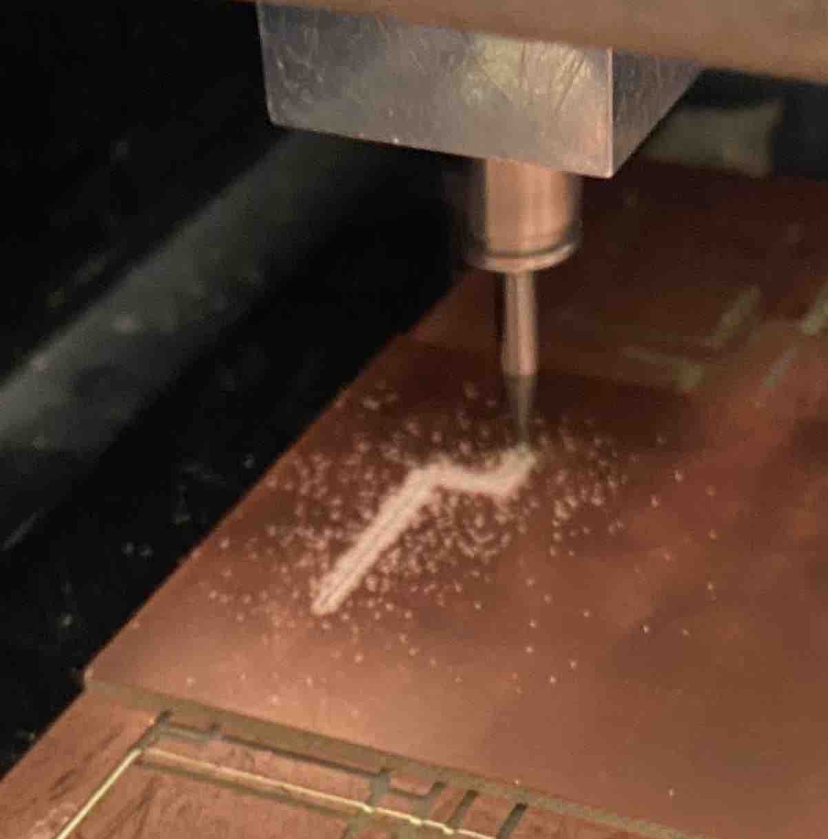
Oops
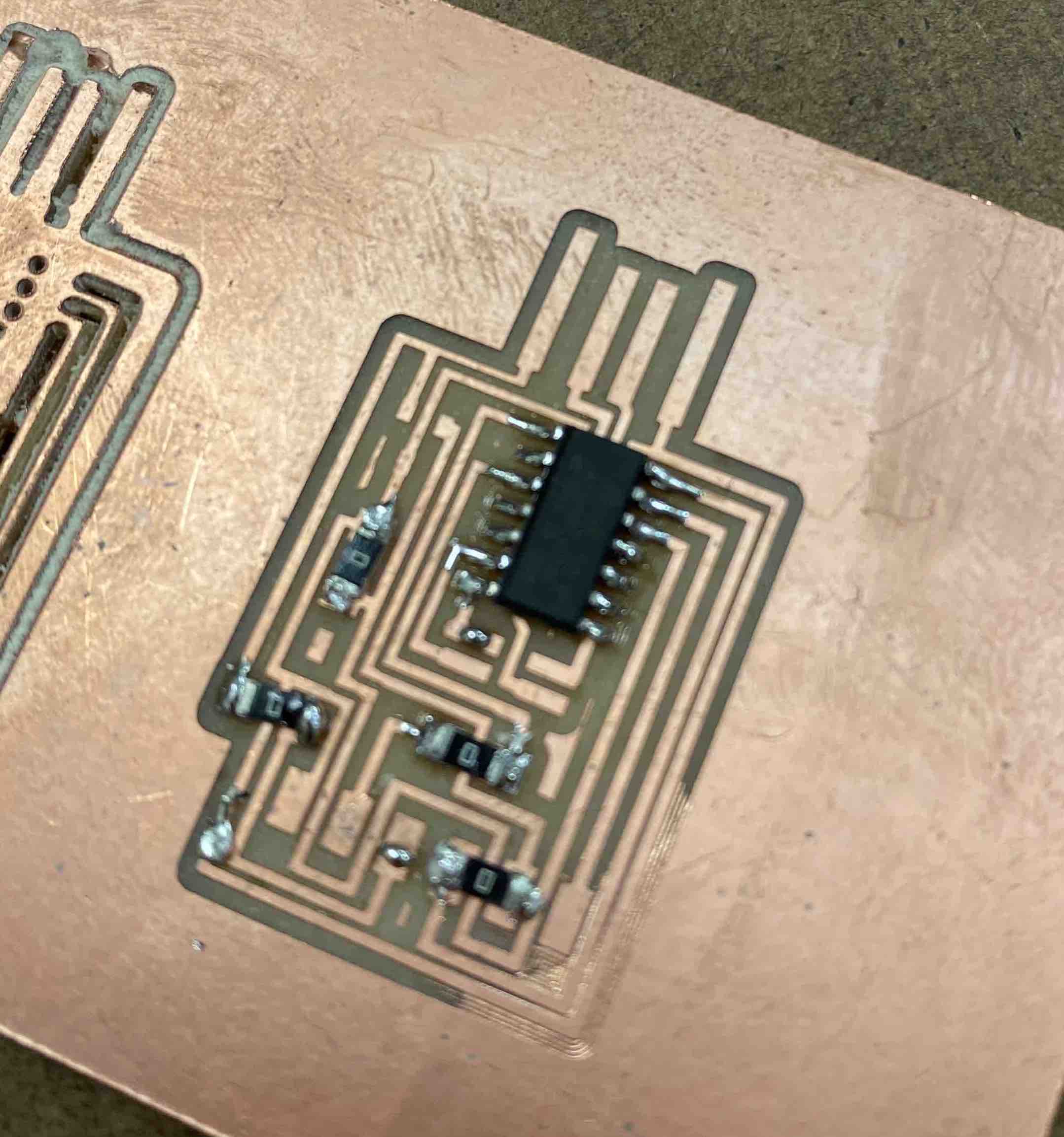
The board wasn't level (I let slide a few bubbles in the tape underneath) -- and this yielded the trace in the picture, since the endmill didn't cut through the copper all the way. You can see some other students had used the scrap board for practicing soldering.
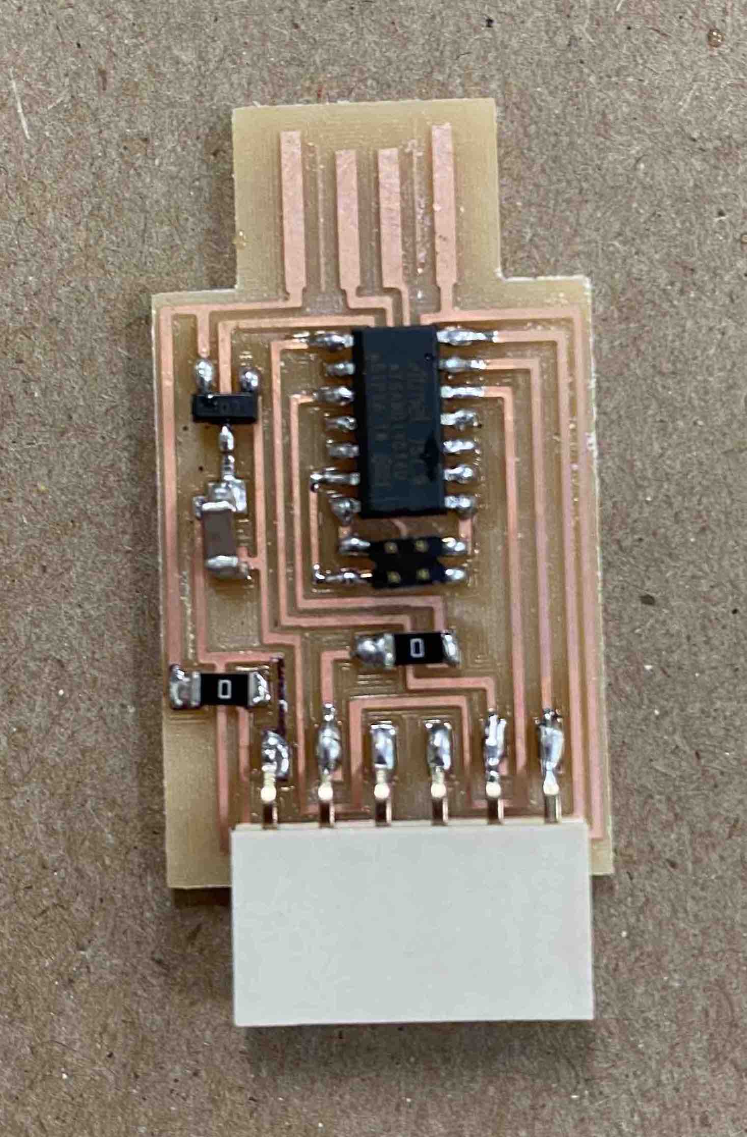
New Board
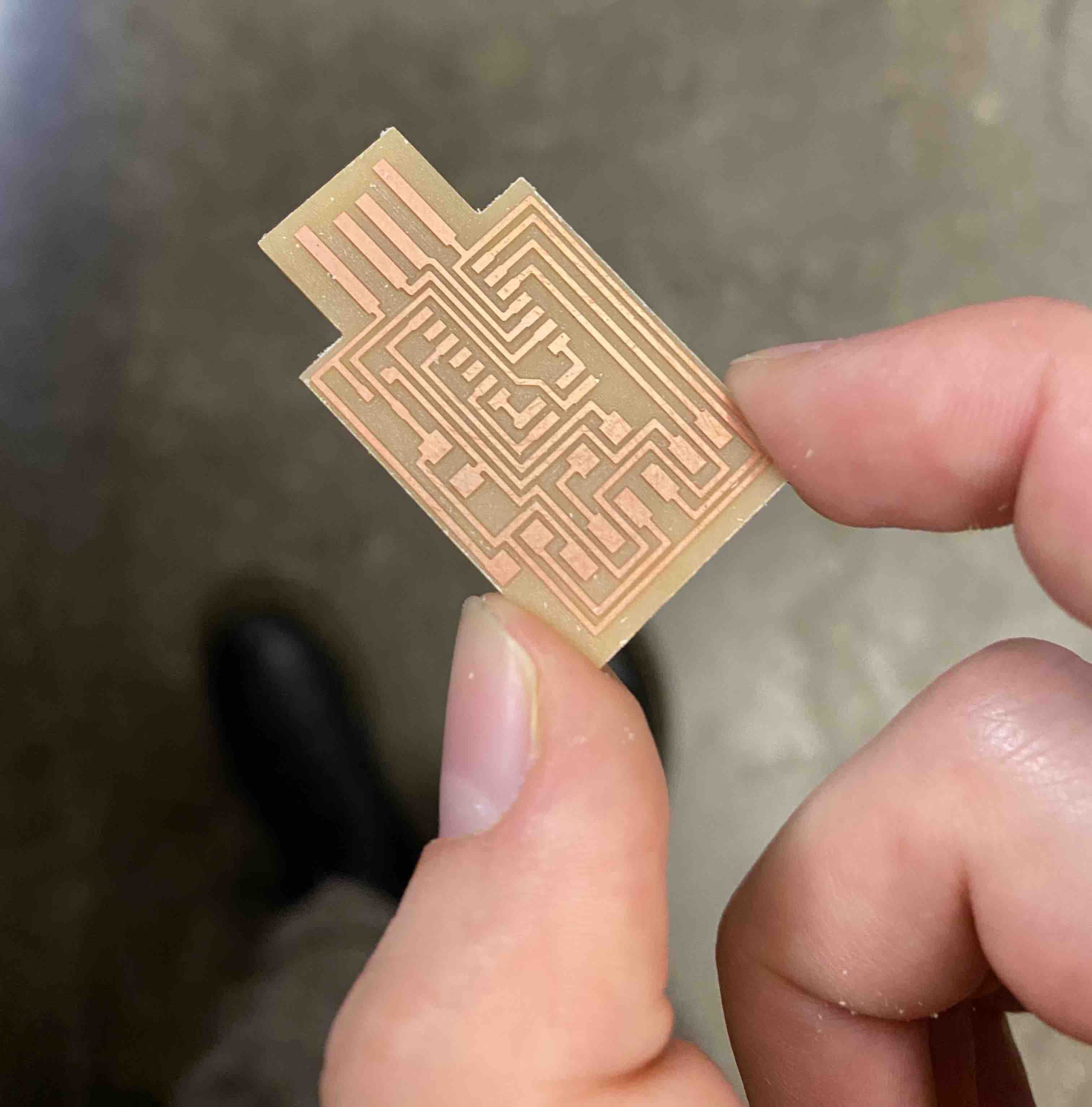
I re-milled the design, this time ensuring the board was level, and got this guy! Very crisp due to the offset of 0.
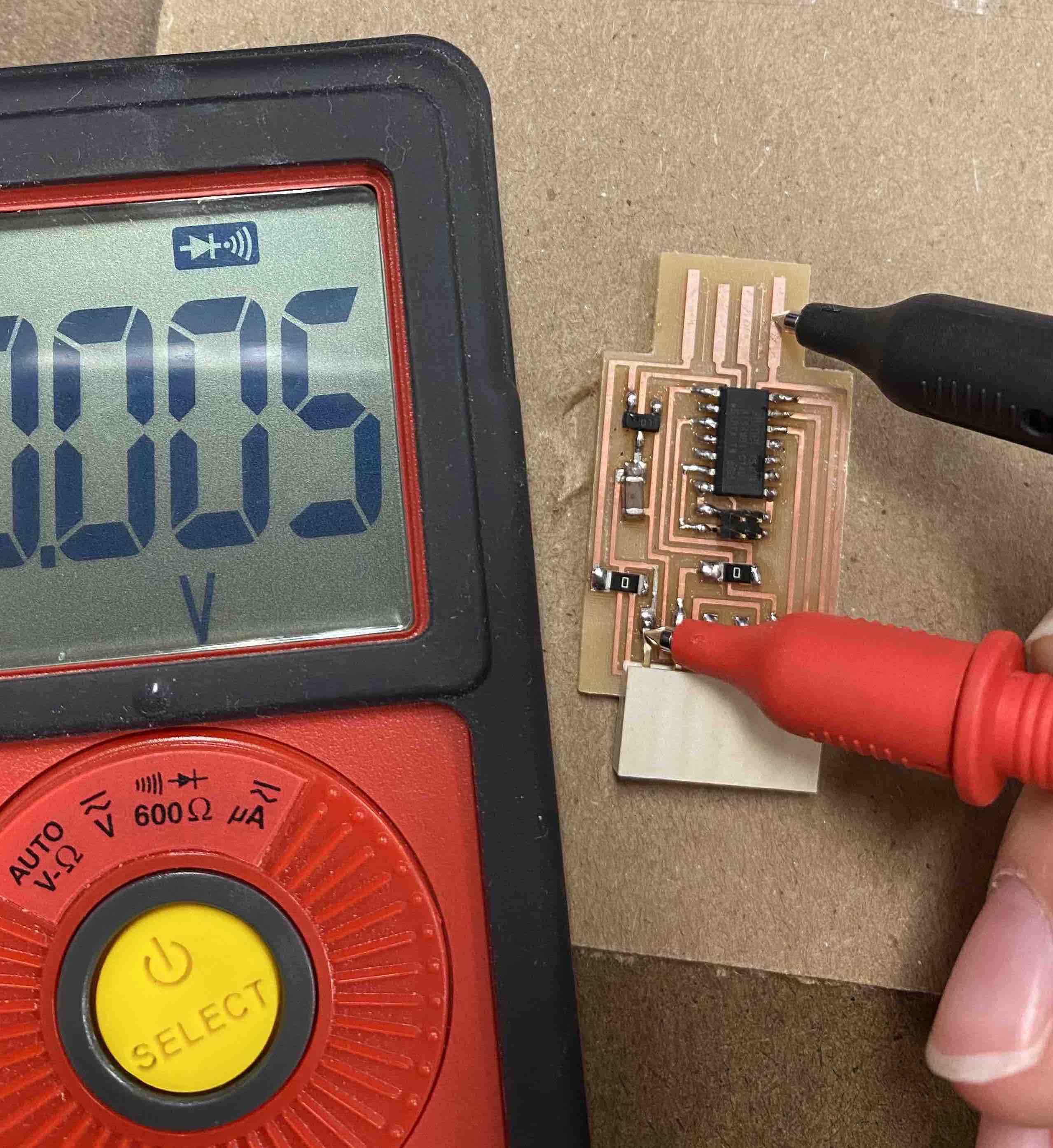
And I'll Need a New New Board
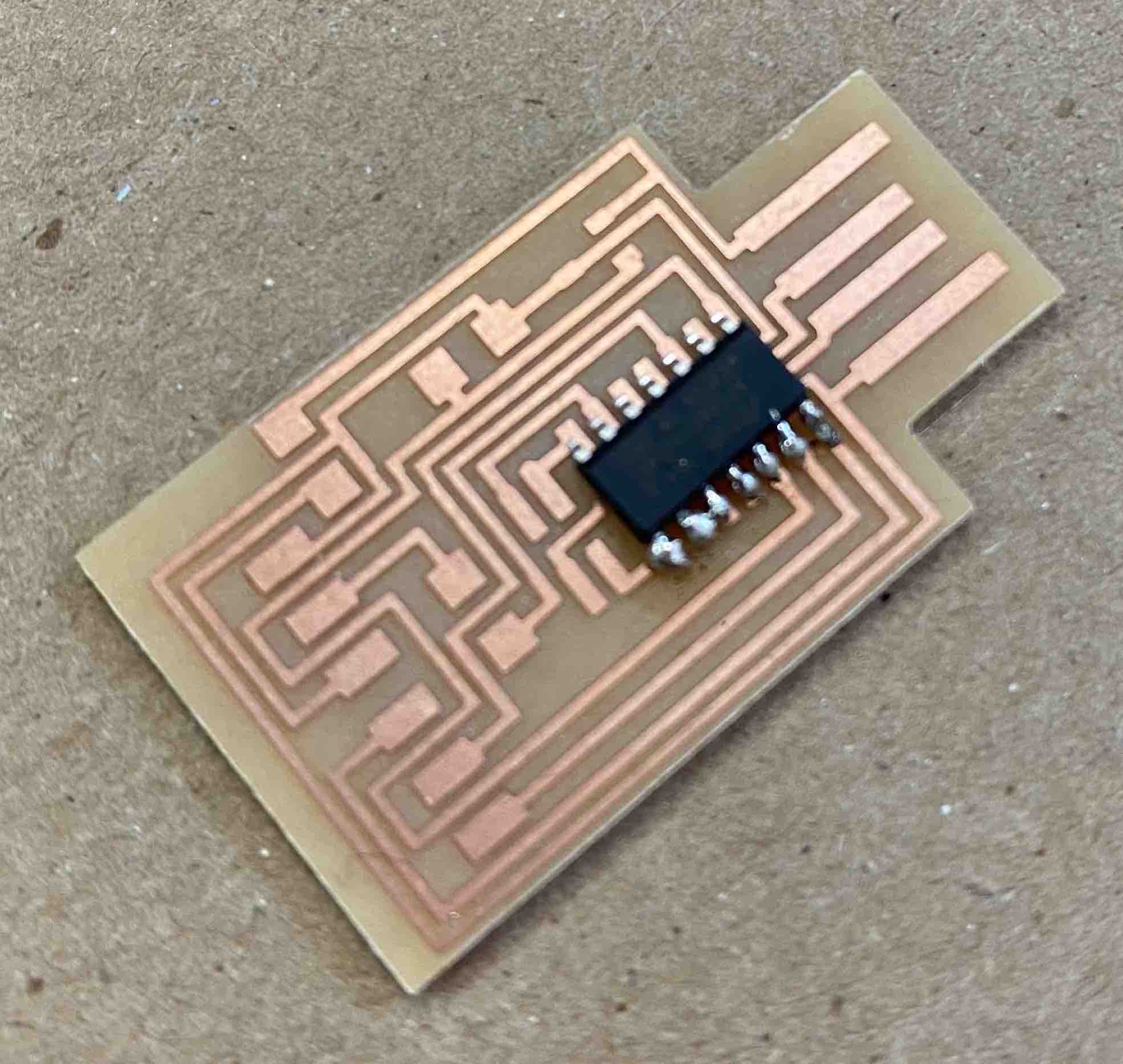
I soldered two pins together by accident, and couldn't remove the solder using the rosin braid -- I was using a type of solder (maybe lead-free) that is notorious (according to the TAs) for taking too long to heat up. I spent maybe 40 minutes trying, but decided it was best to start over.