Project 6: Electronics Production
This week was all about manufacturing PCBs. I used a similar PCB as what I designed last week, but with an accelerometer, the STMicroelectronics IIS3DWBTR Accelerometer.
Let's Start with the Group Project
I started by designing a component to test the design rules for the PCB mill in the REEF, a Roland SRM-20. My goal was to determine the minumum thickness of a slots and traces. On the bottom of the test piece, I have a series of rectangular traces that range in width from 0.001" to 0.020" by 0.001" increments. On the top of the test piece, I made a series of slots in 0.030" squares. The slots had the same width as the the corresponding rectangular traces. See the images below.
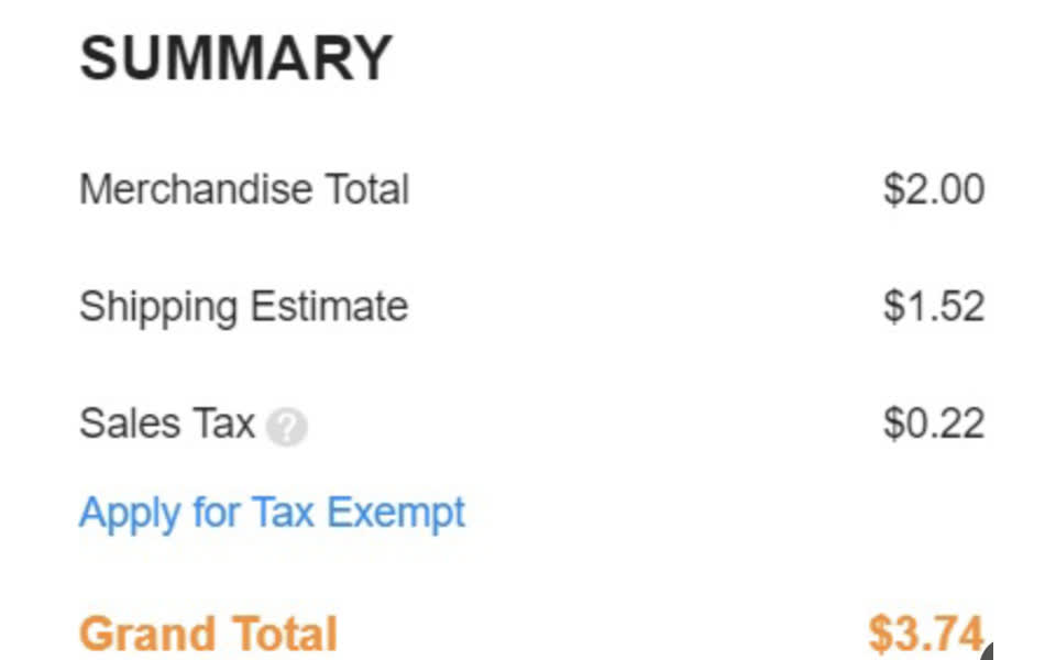
Alex submitted a PCB design gerber file to JCLPCB
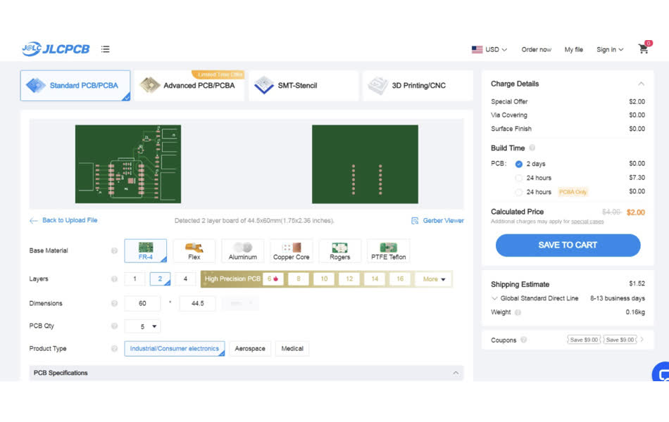
He purchased 5 boards for a whopping $3.74
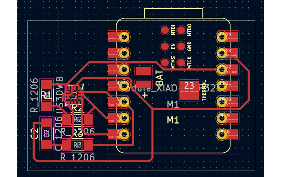
PCB Design: Manufacturing
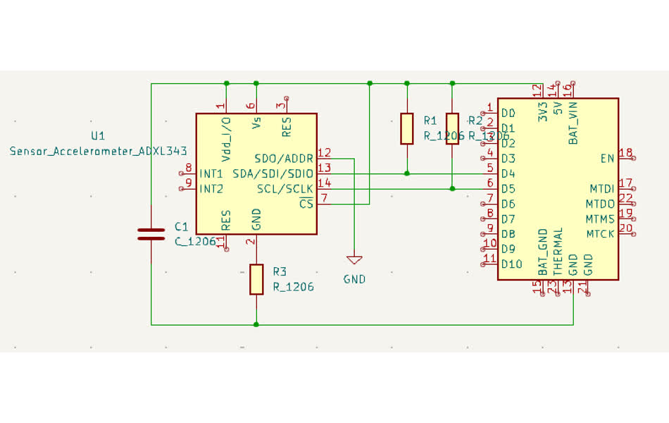
My objective was to make a dev board for my IIS3DWBTR. This thing's downright puny. I'm skeptical about soldering it.
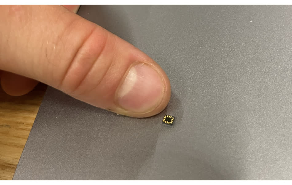
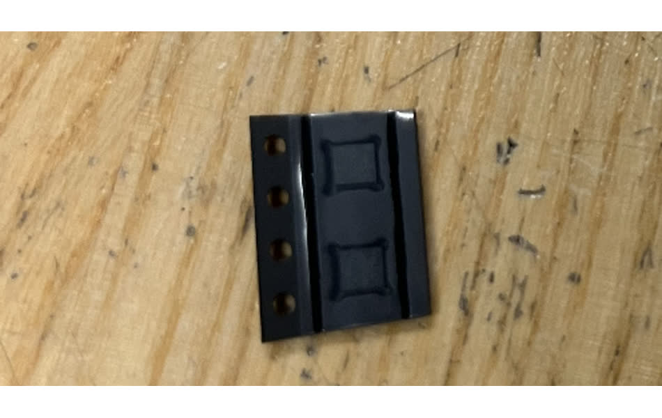
**Funny sidenote: I thought the packaging was the component initially. I was confused where the other 8 pads were, so I asked Leo. He enlightened me.
I used Leo's webmill program to control the Roland SRM-20. I dropped my F_cu and edge_cuts gerber files in the gerber2png website, set the tool location, and milled the board. Sure enough, the tolerances of the mill were not fine enough to accomodate the thin traces and component space requirements of the IIS3DWBTR accelerometer.
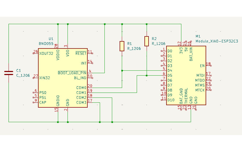
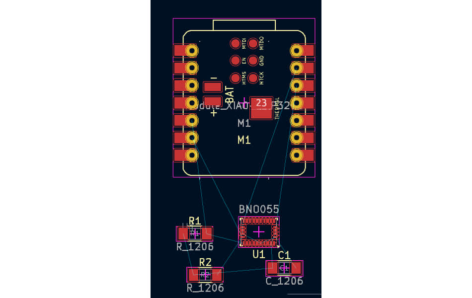
I then upsized to a different accelerometer, sacrificing a lot of performance: the BNO055. This accelerometer is in the fab inventory, so the documentation was less confounding. This accelerometer was pretty chunky, unlike the puny IIS3DWBTR. I found the datasheet and redid my kicad process: sketch the schematic, covert to PCB editor, route traces, gerber2png, Webmill the whole thing. When I was designing the pcb, i realized the BNO055 footprint was much smaller than what was in the lab. I got confused and switched to my third accelerometer after. However the KiCAD process was good practice.
I was confident the 3rd accelerometer, the ADXL343, was going to do the thing. Third time's a charm, right??? RIGHT??? WRONG!!! I started this time by reaching out to Anthony to steal two ADXL343's from MIT. Harvard had none. Anywhere. (I think). The process repeats: sketch the schematic, covert to PCB editor, route traces, gerber2png, Webmill.

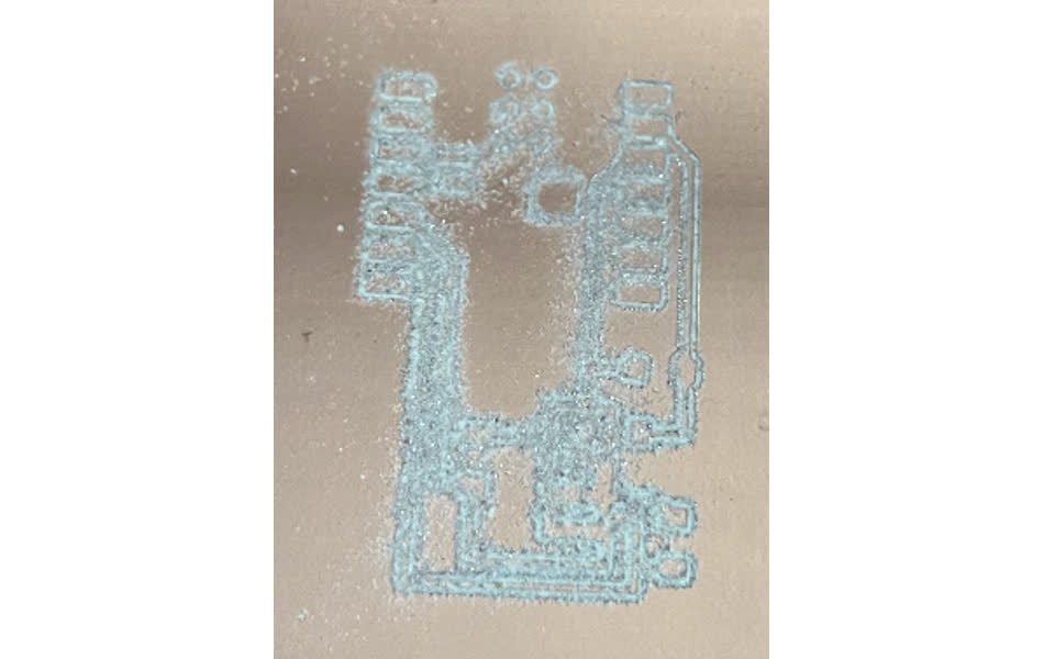
Now it was time to try out the Roland SRM-20 without Leo's help. Not good. Here's where the real problems start. I used my comprehensive notes to do the same process as Leo instructed, or so it seemed. First, I couldn't get the tool to move more than once. Thanks to a sticky note on the Roland, I realized you have to wait 5+ seconds after the tool moves to do subsequent movements. My impatience failed me. After that, I was able to get the trace mill in position: I sent the job, and the Roland went on it's way. It dug deep into the board, and looked very wrong, so I immediately stopped the machine.
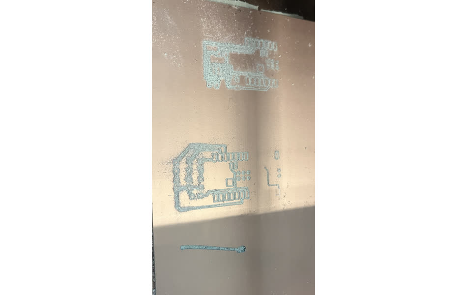
I retried many different times, each time failing for one reason or another. The next board was almost good, but the traces didn't cut through towards the bottom. I think the plate wasn't flat enough
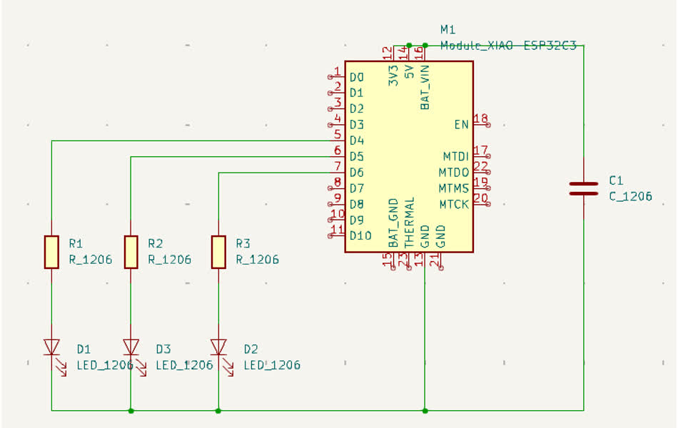
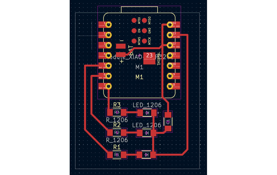
I was ready to give up on the accelerometers and try for a more simple trace with larger tolerances. So I designed an LED stoplight in KiCAD. I figured this would be easier to solder too, if I ever got to that point.
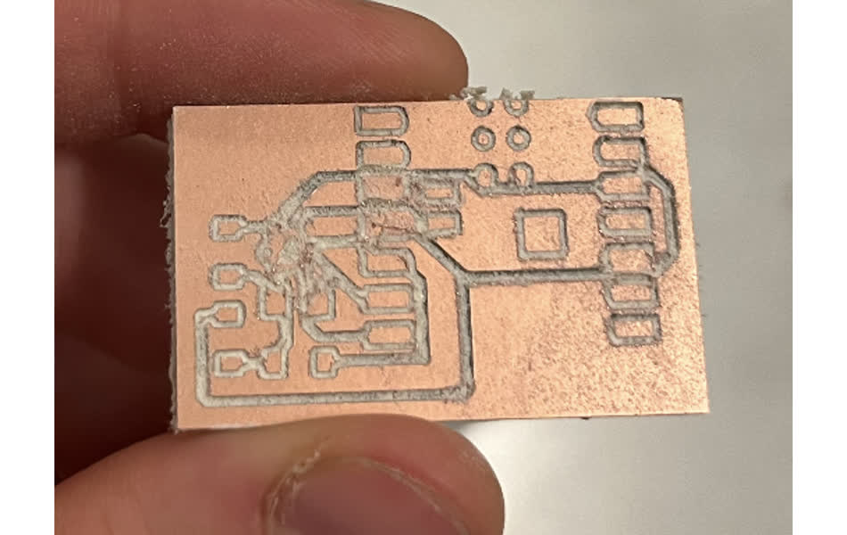
The next day I returned to the Roland: it had defeated be before, but I was optimistic. I redid my not-so-trusty process and sent the job. The trace mill immediately dug almost through the board, and honestly, I'm just surpirsed the bit survived. Check out the gnarly gash below.
I decided it was time to give up on these dastardly boards and retry with Leo's supervision. The Roland was probably just as sick of me as I was sick of it.
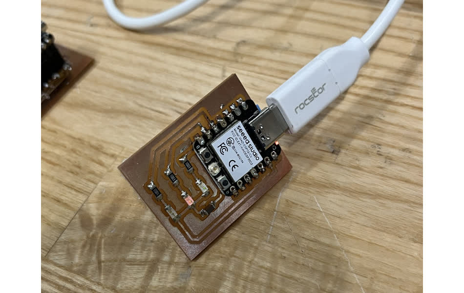
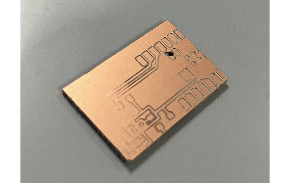
After a long hiatus, I came back to the roland. I re-milled the board with a 1/64 mill and soldered my components.
I made the following script