#4 wire salad
going through this, it was super helpful to talk to some TAs just to better understand what i can and should consider when making my first pcb. while i was in between just exploding the connectors of the seeed xiao esp32, i tried to envision what things i would possibily want to connect. one source that i found was extremely helpful was this fab academy page by adrian torres. it clearly describes and illustrates the thought considerations and design processes that went into a simple extraction and re-organization of the chip pinout to make a more versatile pcb. so i started using Kicad and downloaded the fab library for Kicad including symbol and footprint libraries for the components that have been approved by the TAs. note to future me: make sure you import both libraries, the symbol document as well as the fab.pretty! ...how i started out with a consideration - sketch of top mounted chip to be removed ...first try was overdone - failed attempt ...sketch how i wanted the two chips to communicate
i found it helpful to place the footprint of the xiao esp32 on the schematics sheet and start giving the different
pins labes (and change them as i go and realize what i want and what i dont want to use a certain way).
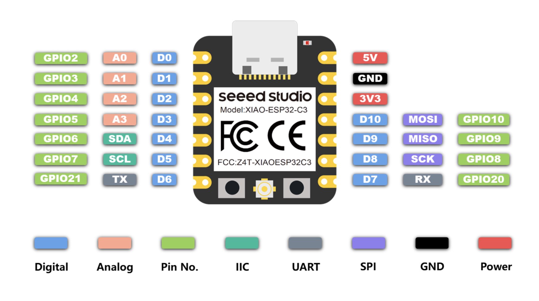
taking another look at the pinout for the chip you use can be very helpful as you look into
other components you want to add to it (here are the links to
seeed xiao esp32c3 and
seeed xiao rp2040
)
that being said, my first attempt was to ambitious, not because it is complex per se, but because i lost oversight super easily
while it all looked clear in my head in the schematic...
...i wasnt able to think through the orientations and connections anymore... so i restarted the process and told myself to keep it simple this time
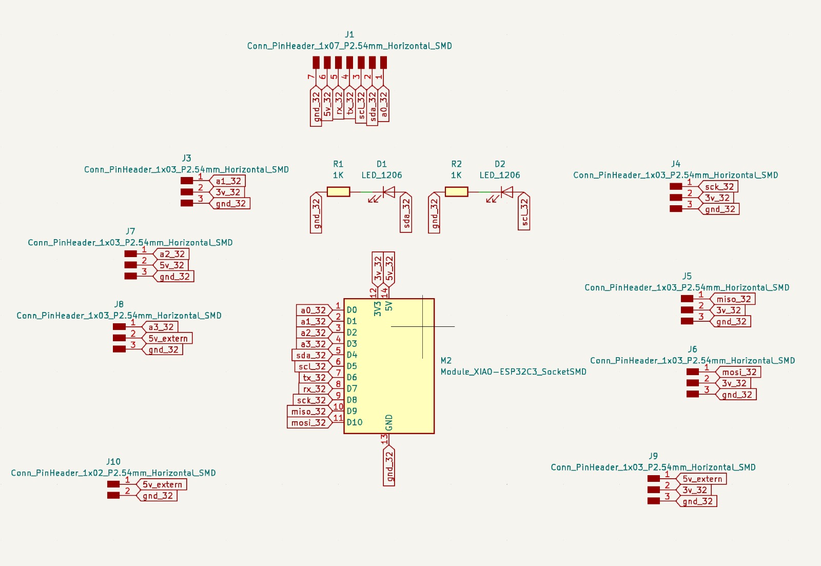
this scheme made a lot more sense to me. i had a couple of pinouts that would allow communication with another pcb with the mirrored pins (to be continued and tested), as well as an led that would blink or a speaker that could use the same signal to buzz when needed, to switch in between these two i placed a switch. additionally, i was looking to implement a button, because the ones on the board are super tiny. something that came through my experimentation with receipt printers, they cannot run of the power supply of the xiao chips, but need their own power supply. i added a screew wire head that does not connect back to the xiao, but alternatively goes to a number of pins, both vertical and horizontal for additional external power supply if needed
from this i was able to wire all the components and check whether my rules still hold true along the design process. some connections needed to shift places to accommodate all the placements and wire thinkesses.
something that was super helpful, was to go back and forth from the schematic to the design builder in Kicad, using the update function every time, to update the new changes in the design editor
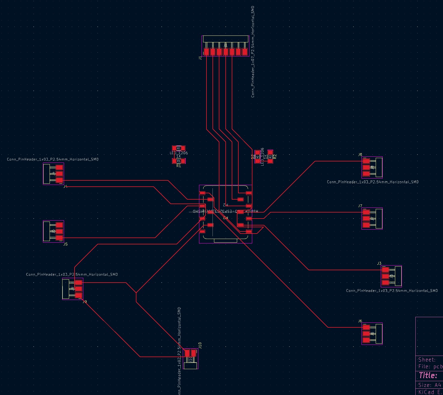
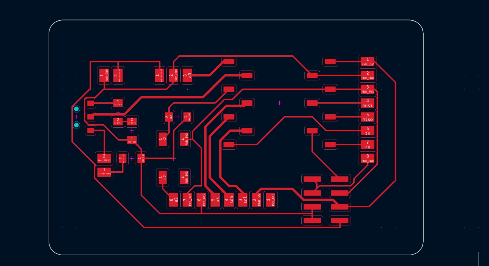
here is my design, this could go terribly wrong but i will not know until i make it and start the process of debugging during the next week. i have not tried any of the addons or plug ins to auto wire, but rather connected all the things things by hand. something that i realized was, it is a lot easier if you start setting the simplest routes first, and work off that point outwards. the simplest connections might need to be replaced and redone eventually again (by going back into the schematic editor and switching labels around) but the simple ones are a lot easier to redo and reroute than the ones that are complicated from the very beginning
here is the KiCad file for this board:
kicad file
when looking at the entire list of sensors and components i could be using for this pcb, there were some components that I would
have loved to use, but i could not figure out how to wire them correctly. therefore i limited myself in this assignment to some
smaller explorations and left the heavy lifting for another week. the reason for this is simply to be able to trace back the
steps i might have gotten fundamentally wrong with simple wiring, before getting into the heavy stuff, and not know where to
start in the debugging process that will follow once it is done.
some components that i used in this example were a little more confusing at first, but it helped looking through their data sheets.
if you place a new component and you are in the library menu, it is quite helpful to click on the link for the respective component
to see what it does, and what pinouts it has/requires. this has saved me a lot of time in figuring out what i want to use, and what
is at this stage still above my knowledge and understanding of electronics
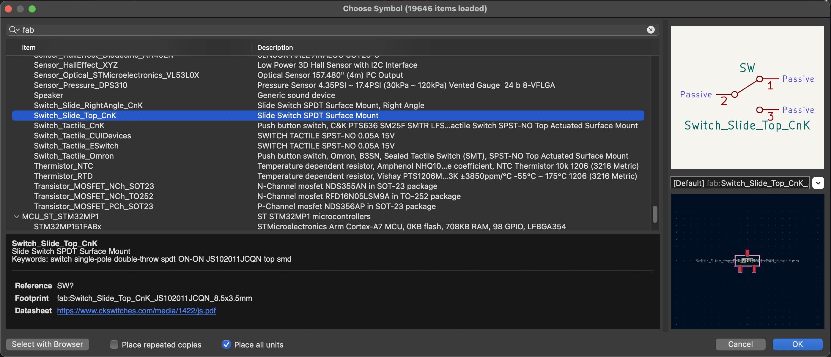
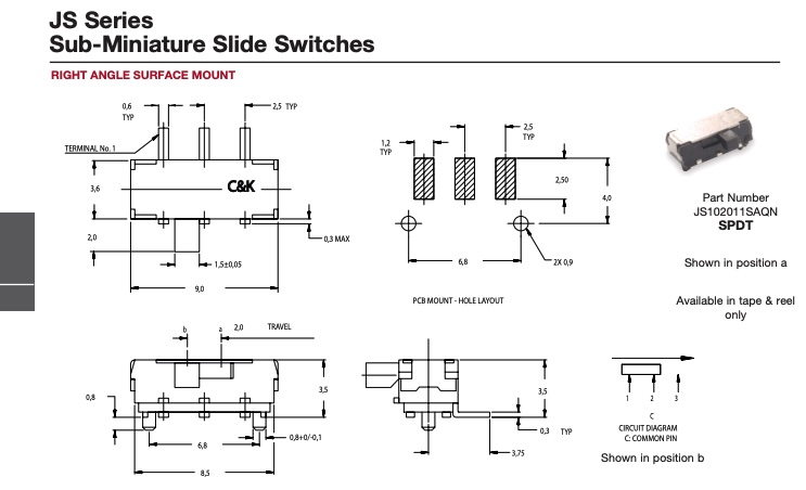
see the link in the bottom of the screenshot, which leads you to the data sheet, often showing a photo of the component as well as different form factors and models of the same component. this is the switch i want to use, moving a signal or to a led or a speaker, depending on what i want to do, but mainly to try the component. also, this switch will require me to drill two holes completely through the board, while everything else will be surface mounted. as far as i understand, the drilling just ensures the stability of the switch, so it does not need to rely solely on the soldering spots for stability.
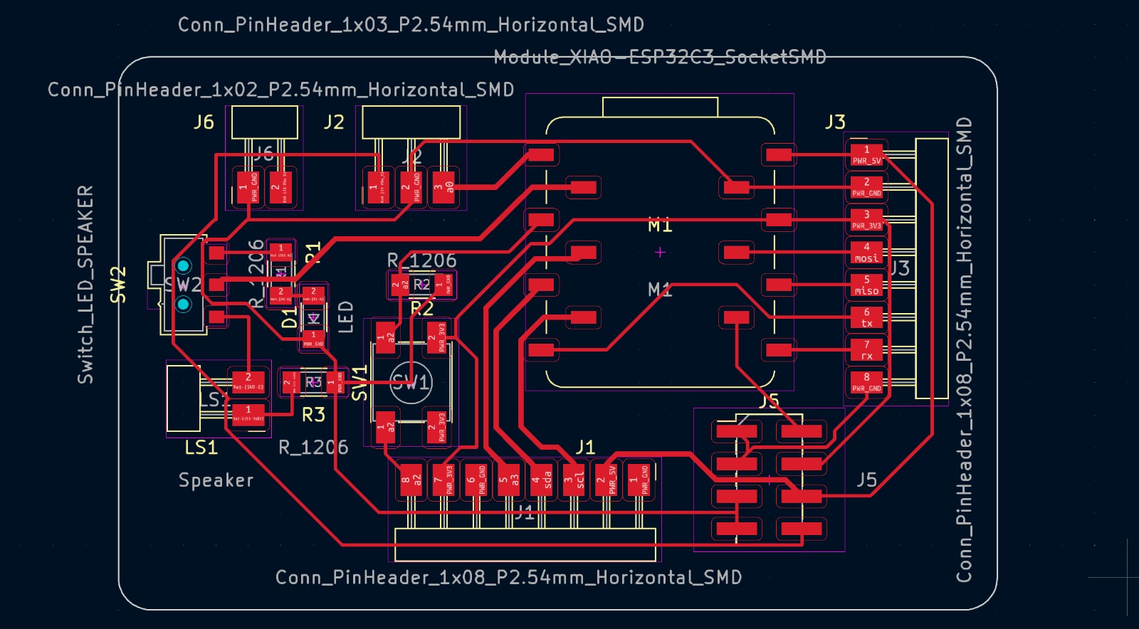
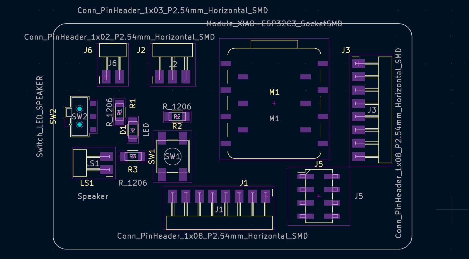
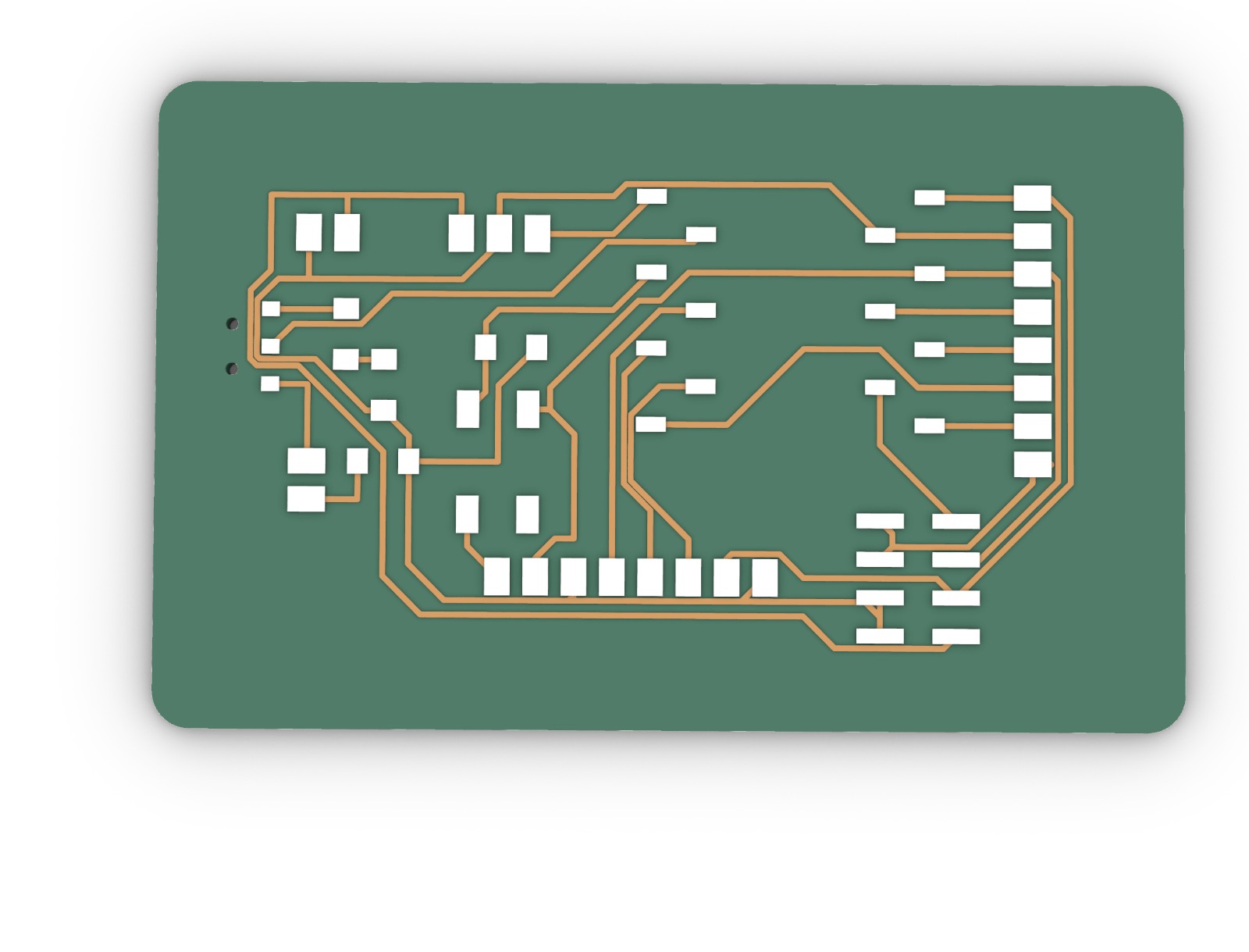
i tried working with the 3d viewer of Kicad itself, which is really pretty, but i went ahead and exported it as a STEP file, to use the 3d file in other software, where i intendto build a case for the pcb eventually. here is a screenshot of the view of the pc board and all the connections I would want/need. this was helpful to just see if i have visually some odd moments on my board, and i assume that there are more than a few spots that might not be working well while milling.
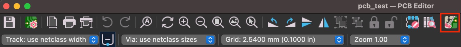
to double check whether the width of the connections are correct, and whether paths are cutting too close to others, it is good to set up design rules in Kicad. these can help when routing the paths, but will also show red arrow and error messages if you checkyour design for it in the design editor.
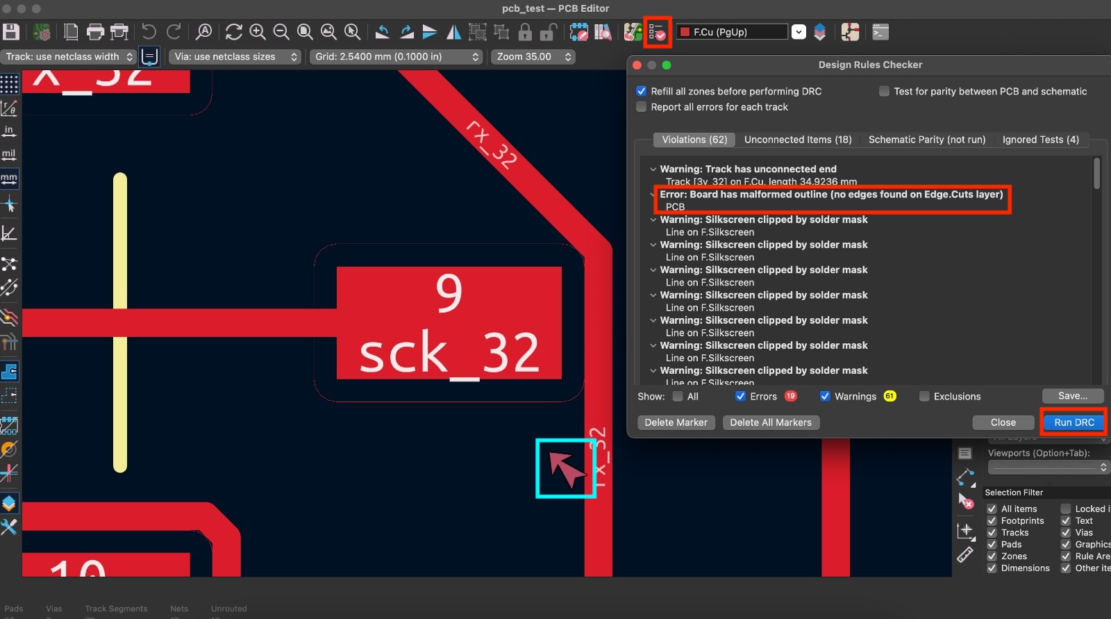
in this example i show where to find the rule checker and the output it generates. the error code it gives me in the console is for a different reason, because i have not specified a boundary for the pcb yet, but there are other errors further below this report window, that would indicate this specific place, which gives me the red arrow. if one cannot see it because of all the lables or one is not sure where to find the specific location for an error or warning on the pcb, one can simply click on the word "error" or "warning" one wants to investigate, and the window will zoom in to the desired location. in this instance, the arrow marks that the path is too close to a pin and that the design rule that i have previously set, that each distance needs to be at least 0.4mm is not possible in this location. i could just redraw the path in this location and run the test again, to see whether the arrow disappears or not.
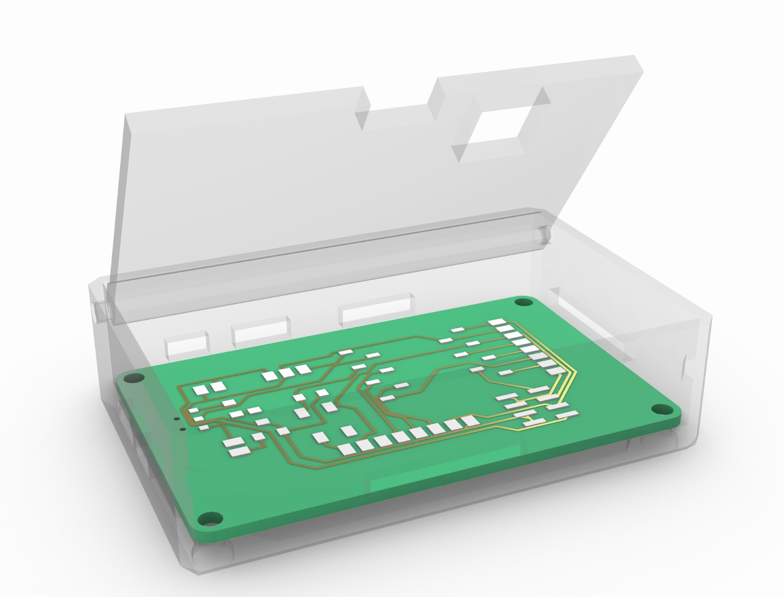
i went ahead and tried to model a quick case for this pcb to be 3d printed. it has a lid that has small corners in the inside of
the box where it could rest on, as well as small inflilled edges on the inside bottom of the box with holes, so i could
technically mount the pcb and fasten it to the box, but then i realized that i have not specified any mounting holes for my pcb yet.
in a next step it might be a good idea to go back into the design and make sure i have mounting holes, but the longer i look at this
box, the more i wish it to look differently, for once, so i can actually connect it to other pcbs, maybe the boxes can lock to
each other, or a system in which the boxes can stack up/the pcbs can stack up inside the box... to be continued
as a group, we met in the shop and looked through the different components available in building 7, trying to understand what is available. we ended up using a multimeter to measure different types of voltage and resistance, both on a bread board prototype as well as using a set of batteries and resistors.
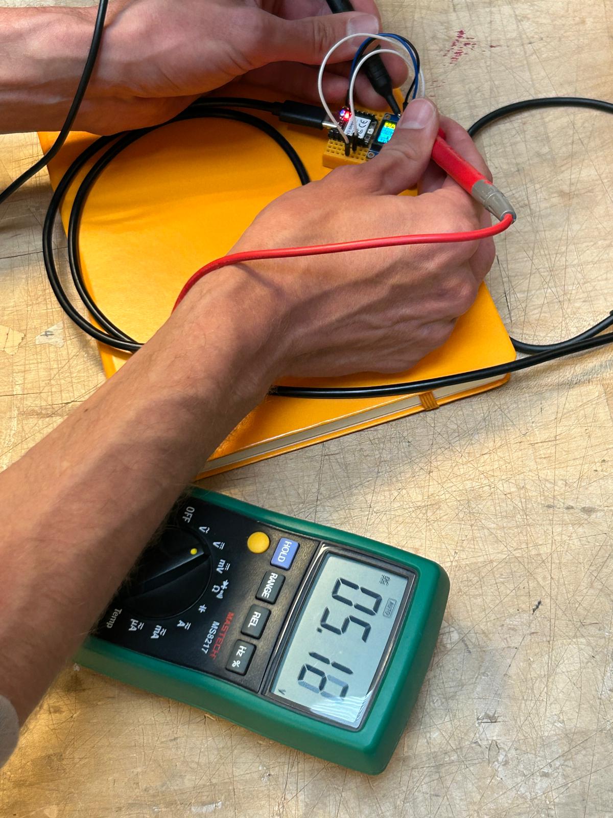
checking voltage coming out of the microcontroller going to the lcd display, that uses 5v to operate.
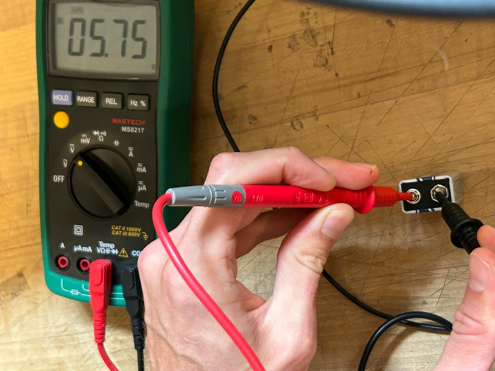
checking a 5v battery
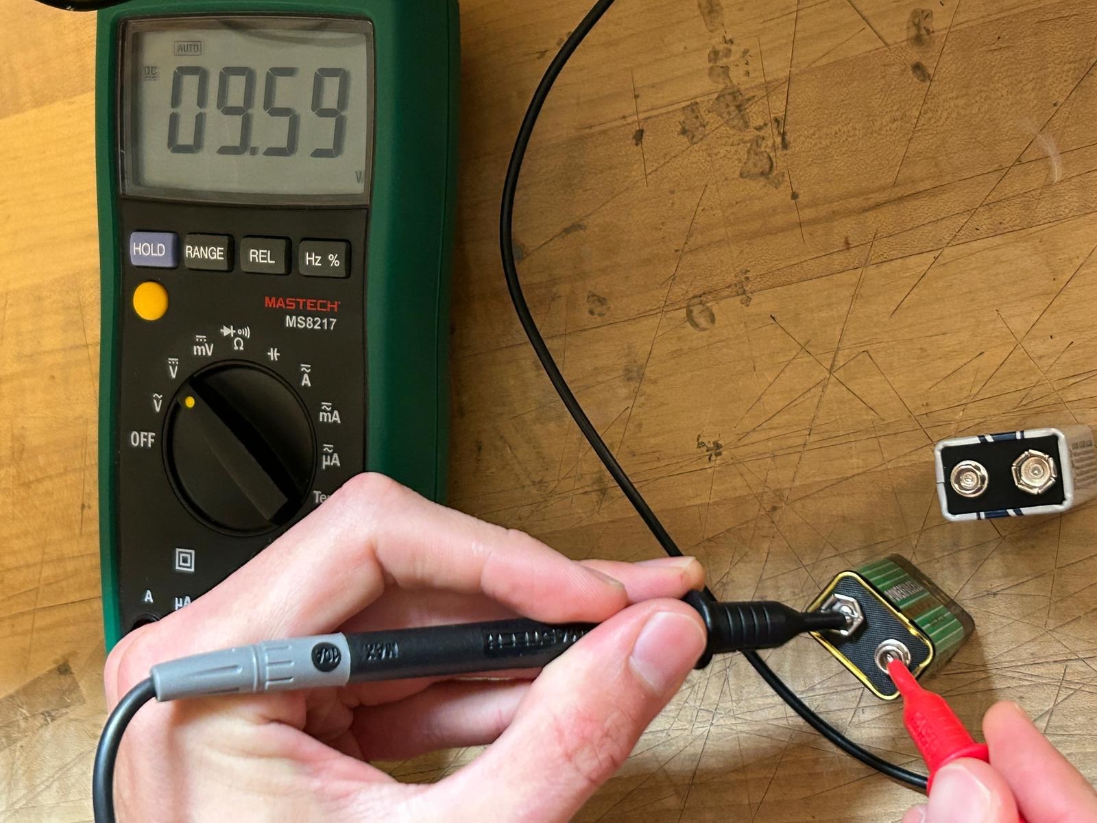
checking a 9v battery
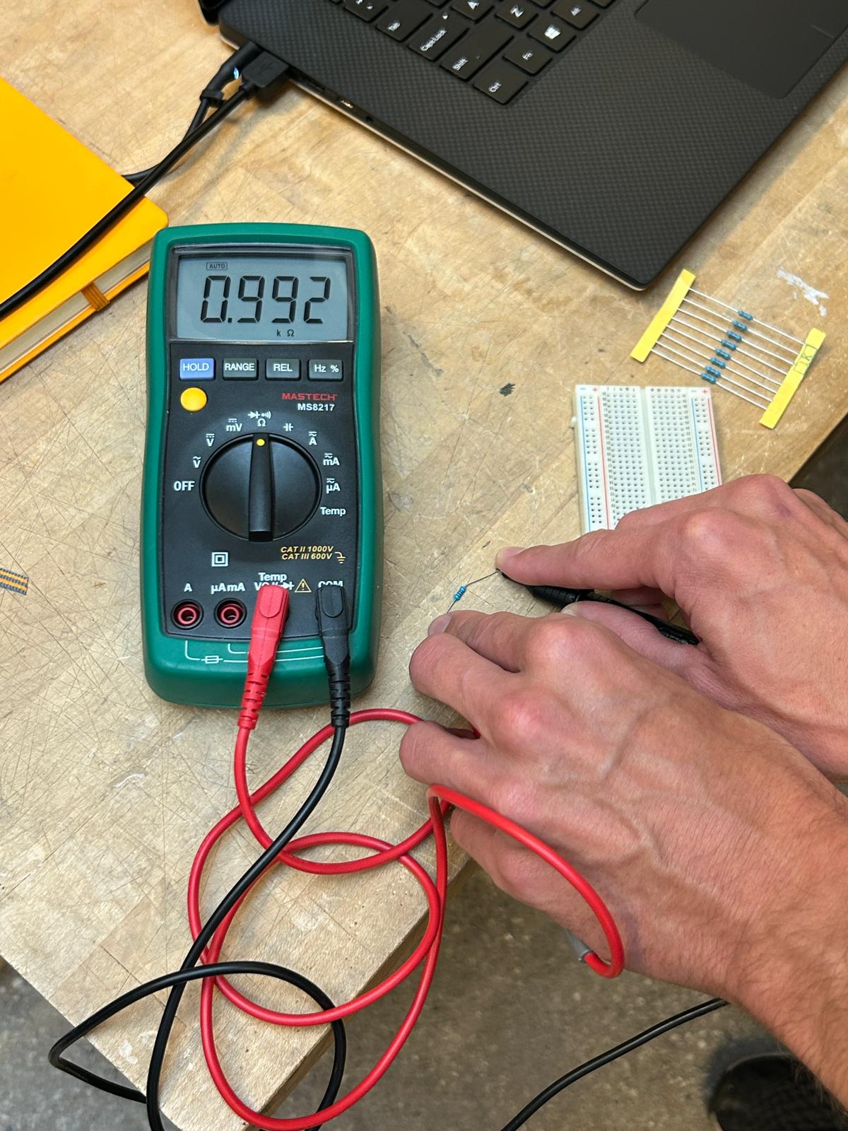
checking a resistor for it's resistance
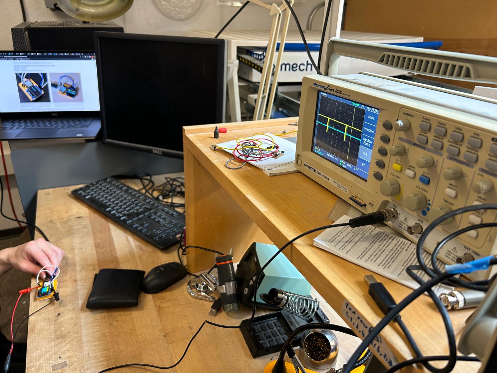
using an oscilloscope to display the waveform that comes into the lcd screen from the microcontroller. setting the oscilloscope to display the impulse, and play with different display and export settings for the recording. i don't pretend to understand what i am looking at, but we played around with it to change its appearance. since we do not know what shape it should have had to begin with, it is difficult to know what we wanted to expect.