I wanted to play with wireless networks, so I bought two XBee radios. Originally I had grander plans to make them do something actually useful with them, but I settled on making small interface boards to test simple communication.
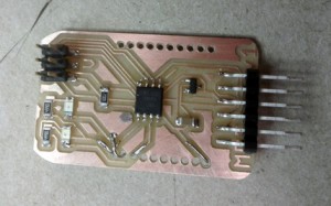
The first board I made had an ATtiny45 to talk to the XBee. The XBee runs at 3.3V, so instead of level-shifting the communication, I just ran the ATtiny at 3.3V. That means the FTDI header is 3.3V too. However, I did put a regulator on the board, so ISP and FTDI VCC are regulated.
Unfortunately, the alternating-pin SMD headers in the inventory are too big for the XBee pins. I resorted to making a through-hole design, which isn’t as nice. The Sparkfun Eagle library has parts for both versions.
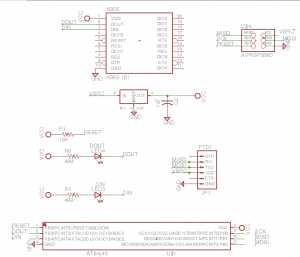
Schematic:
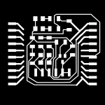
I didn’t have the patience to lay out a nice arrangement manually, so I picked decent spots for the components and let the autorouter do the rest. It did okay, but I had to leave aggressive spacing parameters to complete a single-layer design.
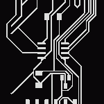
Traces:
Holes:
Board:
I shrunk the tool width setting until the traces resolved themselves.
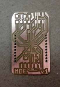
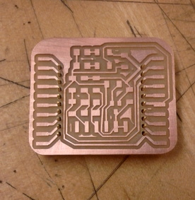
Milled board:
I zeroed too high in the stock and it cut off the top of my board. I just lose an LED connection, so I decided to go with it to save time and copper.
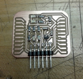
Stuffed board:
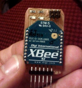
With the XBee module added:
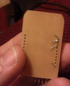
Soldering the pins to the top layer with the XBee on top was quite difficult. To make things worse, the small traces going to some of the pins started peeling. I ran wire pieces to join those traces, and soldered them to the XBee pins on the back side:
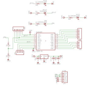
I wasn’t too happy with this board, so I made some changes for the second unit. I decided to design a simpler breakout board that took the two main serial connection pins of the XBee out to an FTDI header. This was inspired and based on the Sparkfun and Ladyada breakout boards.
This time, I did level-shifting on the input pin so that 5V could drive the 3.3V to the XBee. I used a voltage divider for this. For the output, I left it as 3.3V instead of doing anything tricky. Various sources (and my later experience) say that will still register as high with most 5V logic. I also brought out all the pins to pads for possible use of more XBee features. I put the XBee on the back of the board so that I could solder the pins to the top layer more easily.
Schematic:
Traces:
Holes:
Board:
Milled board:
The trace on the right side is for the signal strength (RSSI) LED, so it can be eliminated if desired, making the board skinnier.
You can two pads above the FTDI connector where a nearby trace completely merged with the pad. I resolved those two with board surgery.
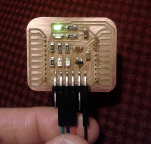
Stuffed board:
Connected to the computer, with power LED illuminated:
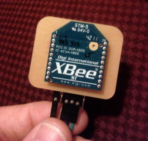
XBee on the back of the board:
I realized that the Sparkfun schematic I was consulting reversed the RX and TX pins of the FTDI header, so I had to use jumpers to fix that problem. Sparkfun did that to allow wireless boatloading, which I could probably explore if I made another (paired) one with correct pins.
After a few tries, I could connect to the breakout board with the Arduino serial monitor at 9600 baud (the XBee default). The trick is to get line breaks correct (read the datasheet!). The “+++” string to enter command more needs nothing else, but subsequent commands need carriage returns at the end.
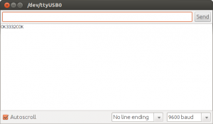
Talking to the XBee:
I sent +++, ATID, ATCH, then +++ (the responses are concatenated together without linebreaks).
I programmed the tiny45 board to send strings over the XBee, but it isn’t working… I suspect a bad connection with all of my wire grafting nonsense. I used Arduino to simplify the software serial communication. You have to use SoftwareSerial instead of Serial since the ATtinys don’t have hardware UARTs. I followed David Mellis’s instructions, which worked nicely. Alert! Be aware that the pin numbers on the tiny chip aren’t the same for the physical ports. Check the variants folder. For the tiny45, it’s now:
//                +-\/-+
// Ain0 (D 5) PB5 1|   |8 Vcc
// Ain3 (D 3) PB3 2|   |7 PB2 (D 2) Ain1
// Ain2 (D 4) PB4 3|   |6 PB1 (D 1) pwm1
//            GND 4|   |5 PB0 (D 0) pwm0
//                +----+

