Electronics Production
Milling, Soldering, and Programming a PCB (Printed Circuit Board)
Characterizing the milling machine
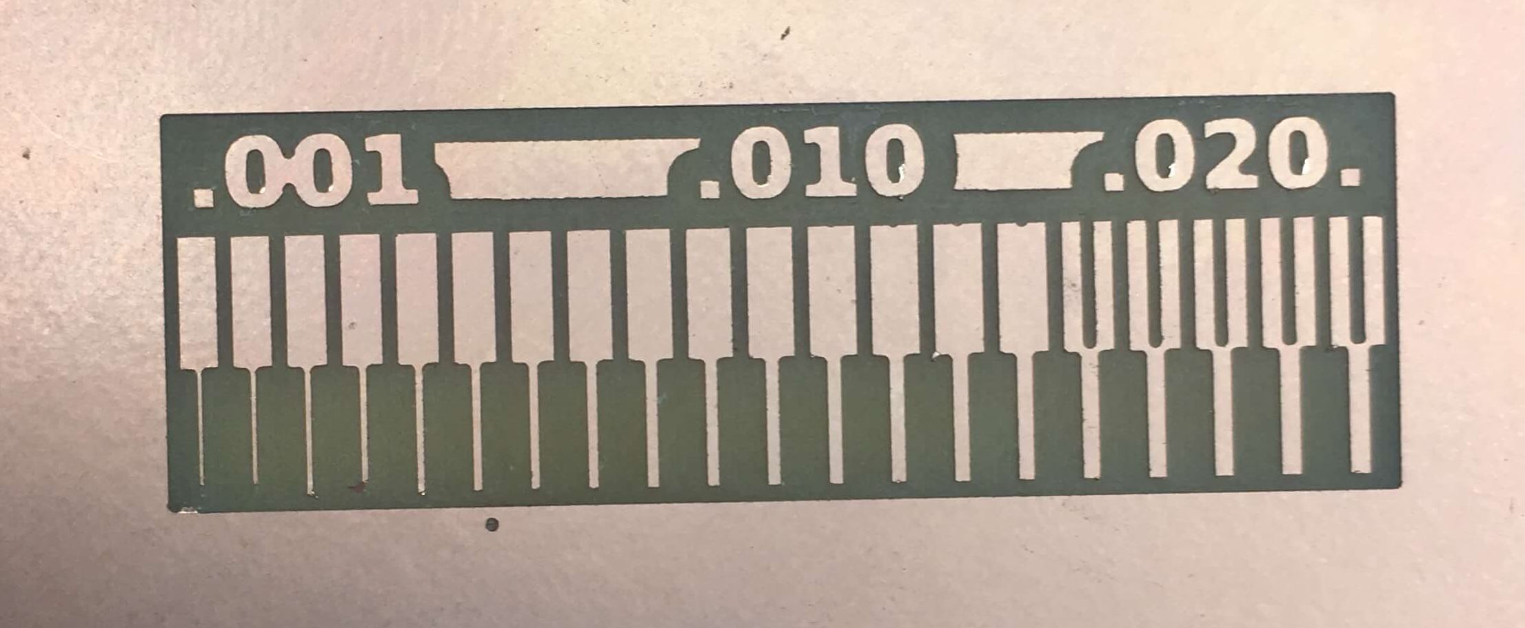
First in order to understand the milling machine and how thin the traces could get, we characterized the board and determined that around .05" the mill became slightly unreliable.
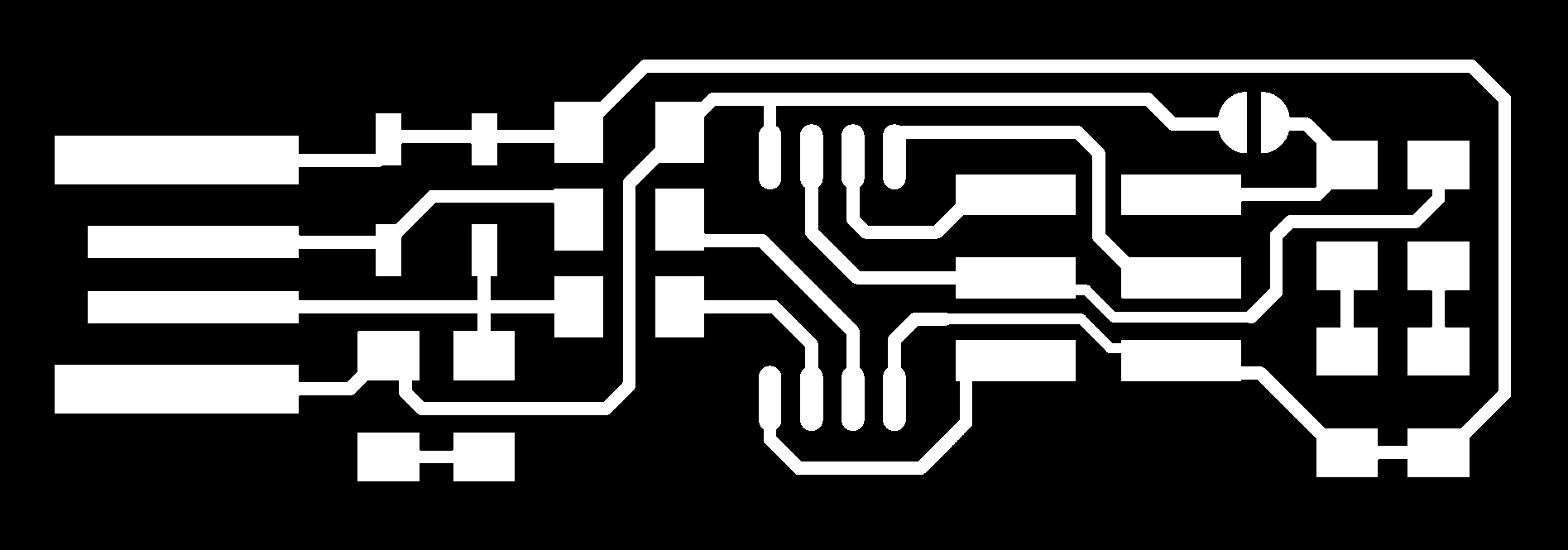
I created the board that was linked for us to create here.
For this assignment I didn't use Eagle to create the board but used the images
provided to mill the traces and cut the outline of the board by uploading it to the mods software. Therefore I didn't need to worry about trace thickness in Eagle for this specific board as the image was already provided.
Milling the PCB

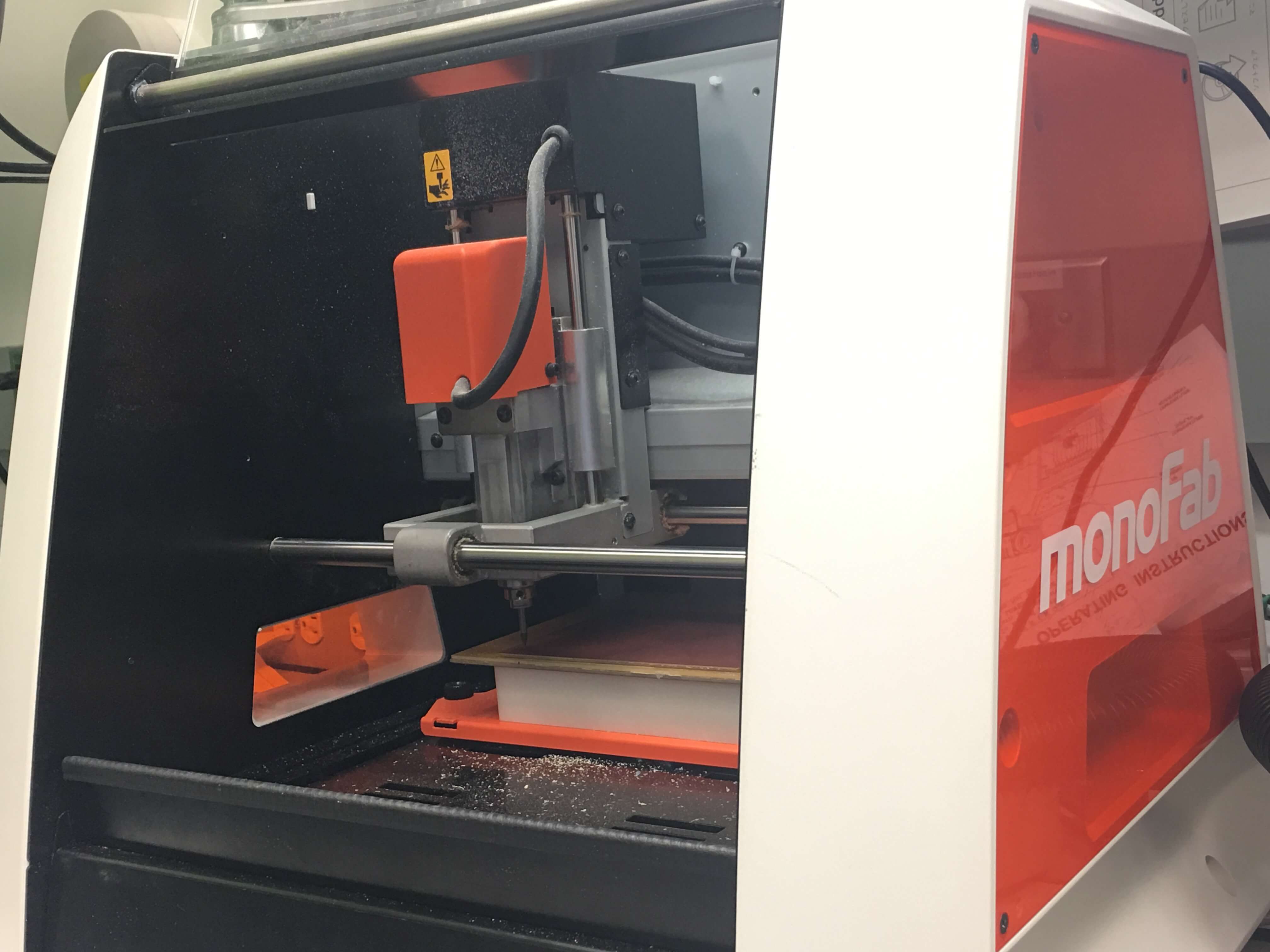
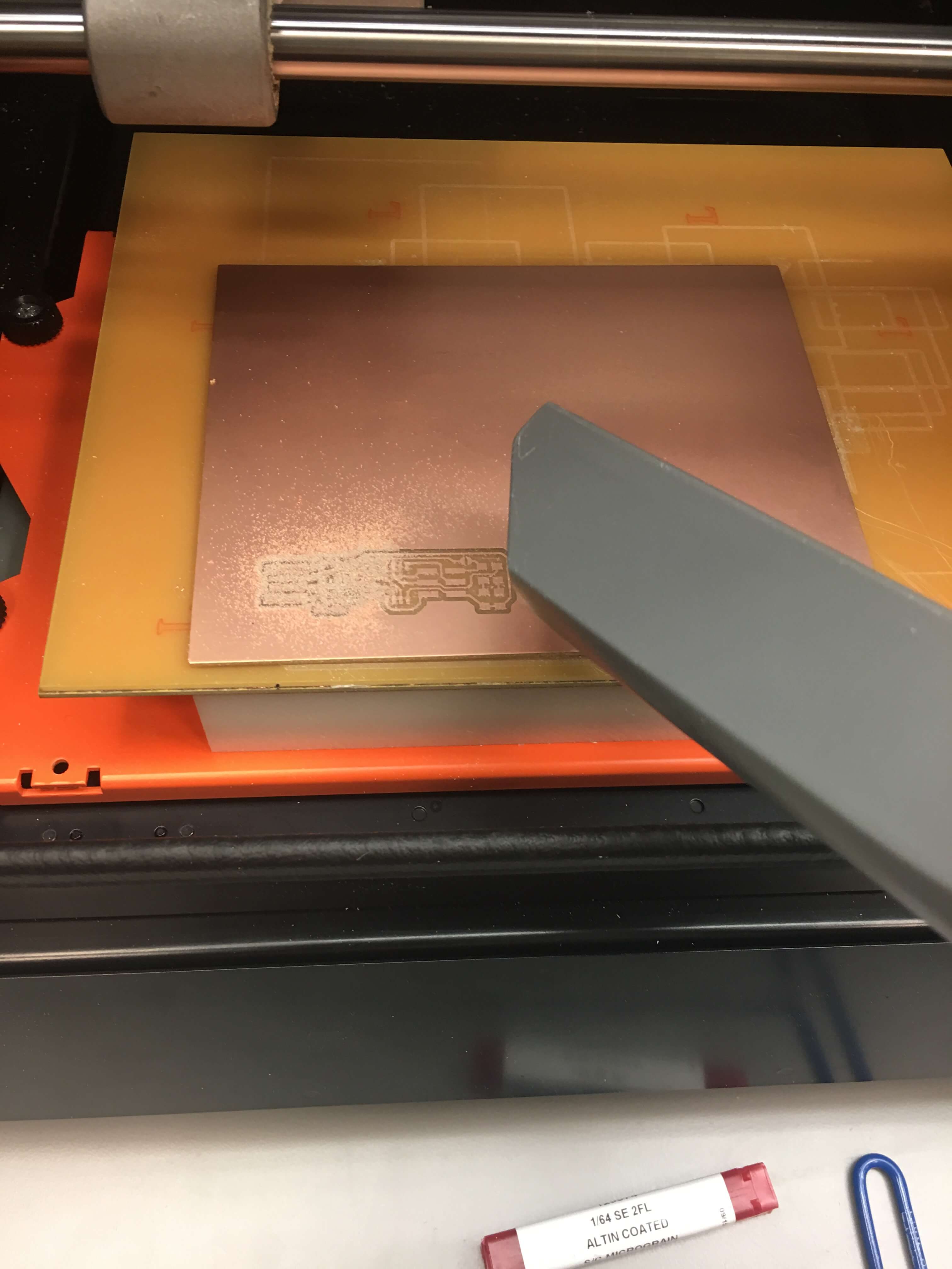
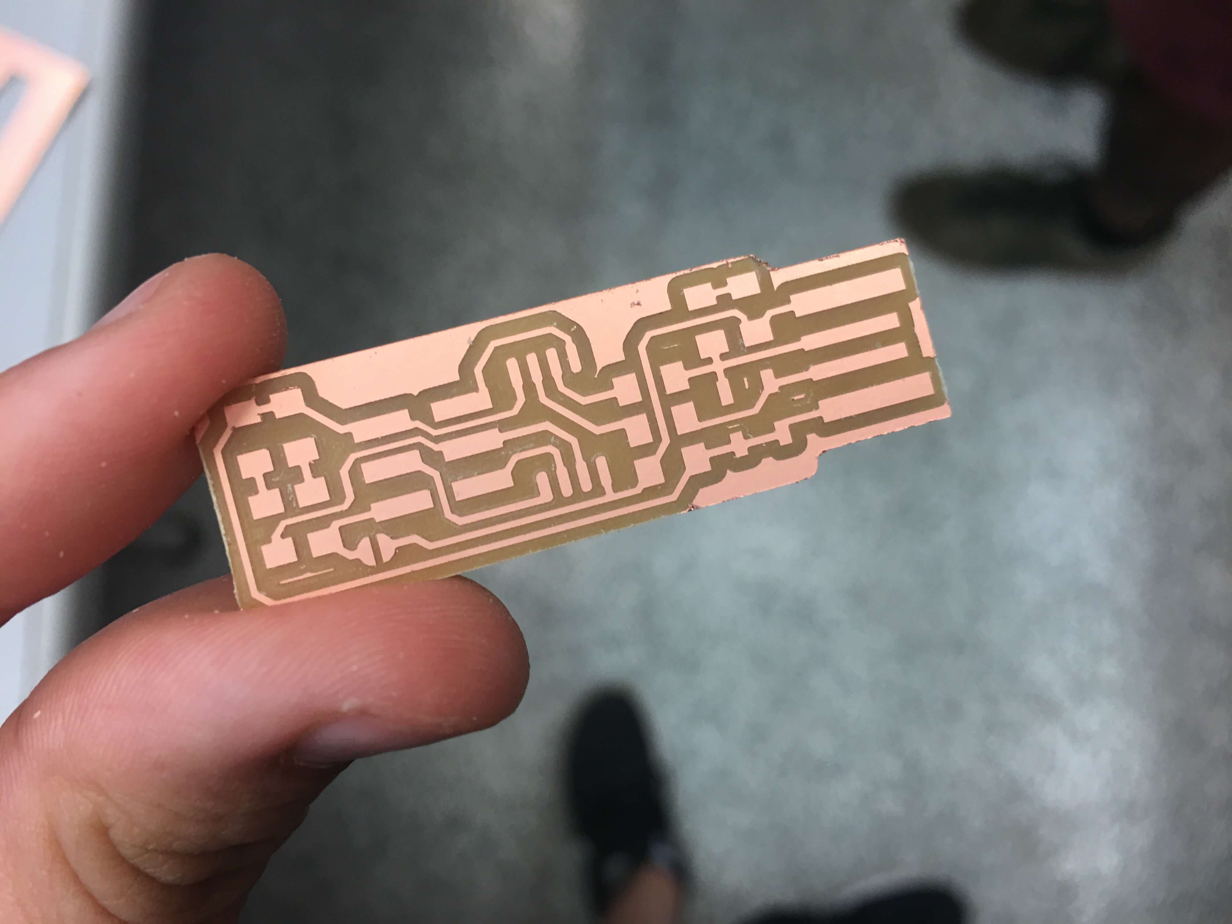
Then I milled the traces using the MonoFab machine vacuuming in between milling the outline and traces to remove dust, and removed the extra copper off of the tip of the PCB.
Soldering the PCB Components
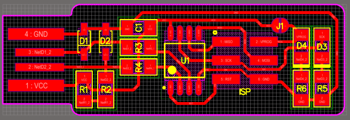
Following schematic provided to us, I gathered the following materials:
- 1x ATtiny45
- 2x 1kΩ resistors
- 2x 499Ω resistors
- 2x 49Ω resistors
- 2x 3.3v zener diodes
- 1x blue LED
- 1x white LED
- 1x 100nF capacitor
- 1x 2x3 pin header
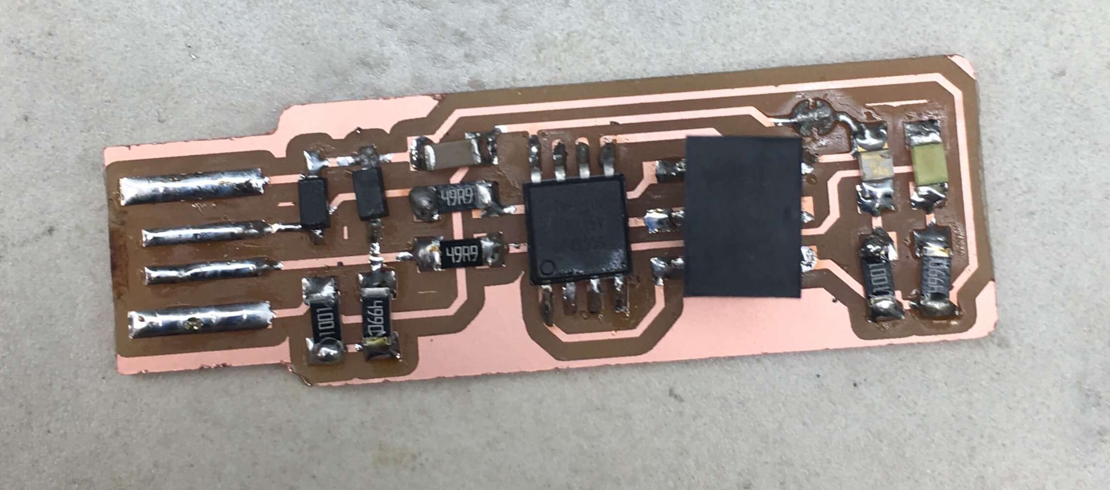
and soldered on the components and flowed some solder over the USB connector copper traces to improve the connection! As you can see from the soldering, not all the joints are completely smooth and some of the solder is bearing some of the weight of the ISP. This was my first time soldering, and while I found it relaxing, it was also challenging.
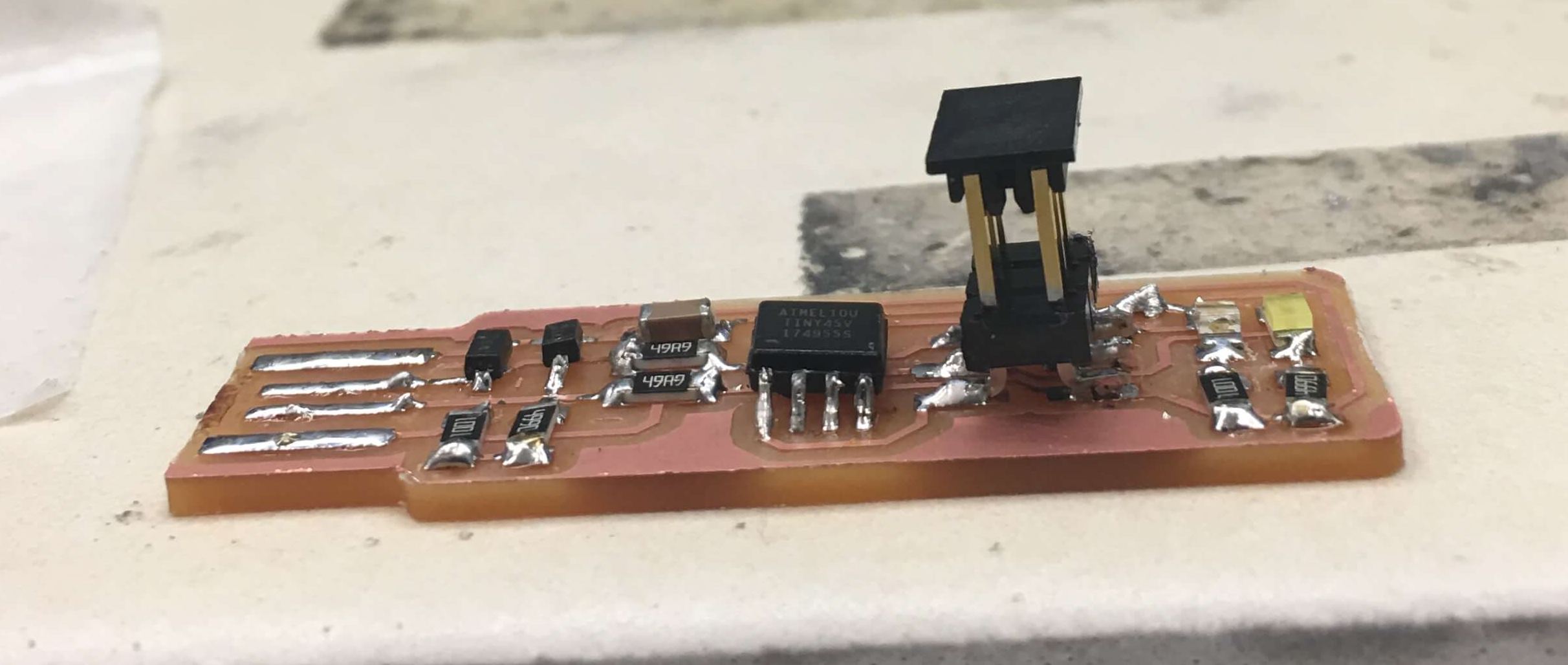
Programming the PCB
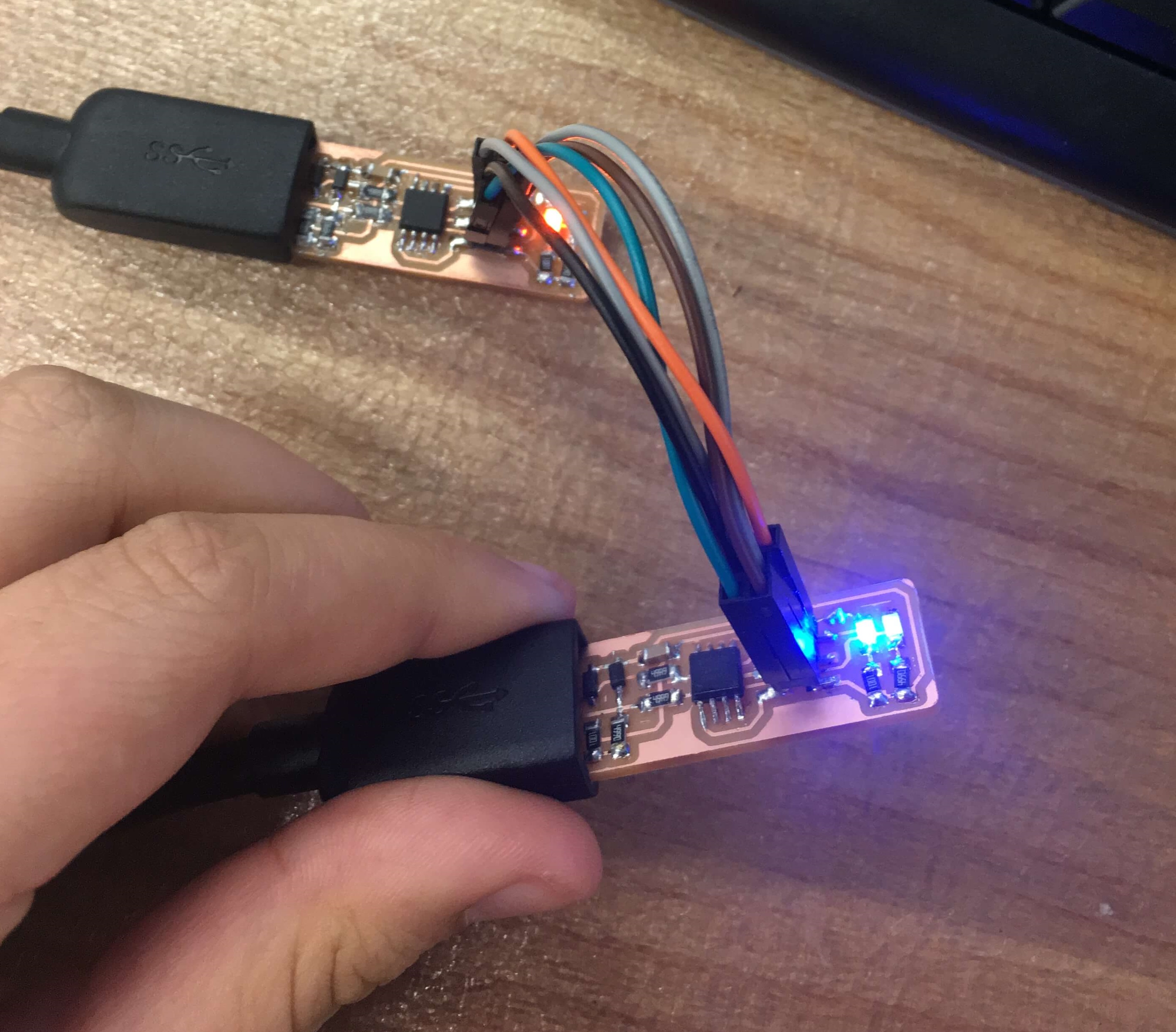
The next step was to program the PCB. I used the lab computer with the required environment already installed to program the PCB. I ran make flash and make fuses and both ran properly without any difficulties. The final step was to blow the reset fuse by running make rstdisbl and disconnecting the VCC from Vprog pin. I used a copper braid to remove the solder and broke the connection.
The blue and white lights on indicated that the programming succeeded!
Important lessons learned:
- When using the mods milling software for the SRX-20 double the DPI when uploading the .PNG file to make sure the board is milled as the right size