Web Design, Version Control, and Final Project Brainstorm
Laser & Vinyl Cutting
3D Scanning and Printing
Make Something Big
Molding and Casting
Electronics Production
Electronics Design
Embedded Programming
Input Devices
Output Devices
Networking & Communications
Interface and Application Programming
Final Project
Group Assignment
The group assignment was to compare the performance and development workflows for other architectures. This was done in collaboration with with Jordan, Maya, Gil, and Emma. The process and results can be viewed here.Embedded Programming
Assignment: read a microcontroller data sheet. Program your board to do something with as many different programming languages and programming environments as possible.
The first thing I did was downlaod and skim through the data sheet for the ATtiny 1614 since that's what I was using and will likely be using in the future.
Last week's board's inefficiencies
So I found out that the board I designed last week would be a bit challenging to work with from a hardware interfacing perspective.The key component is the FT232:
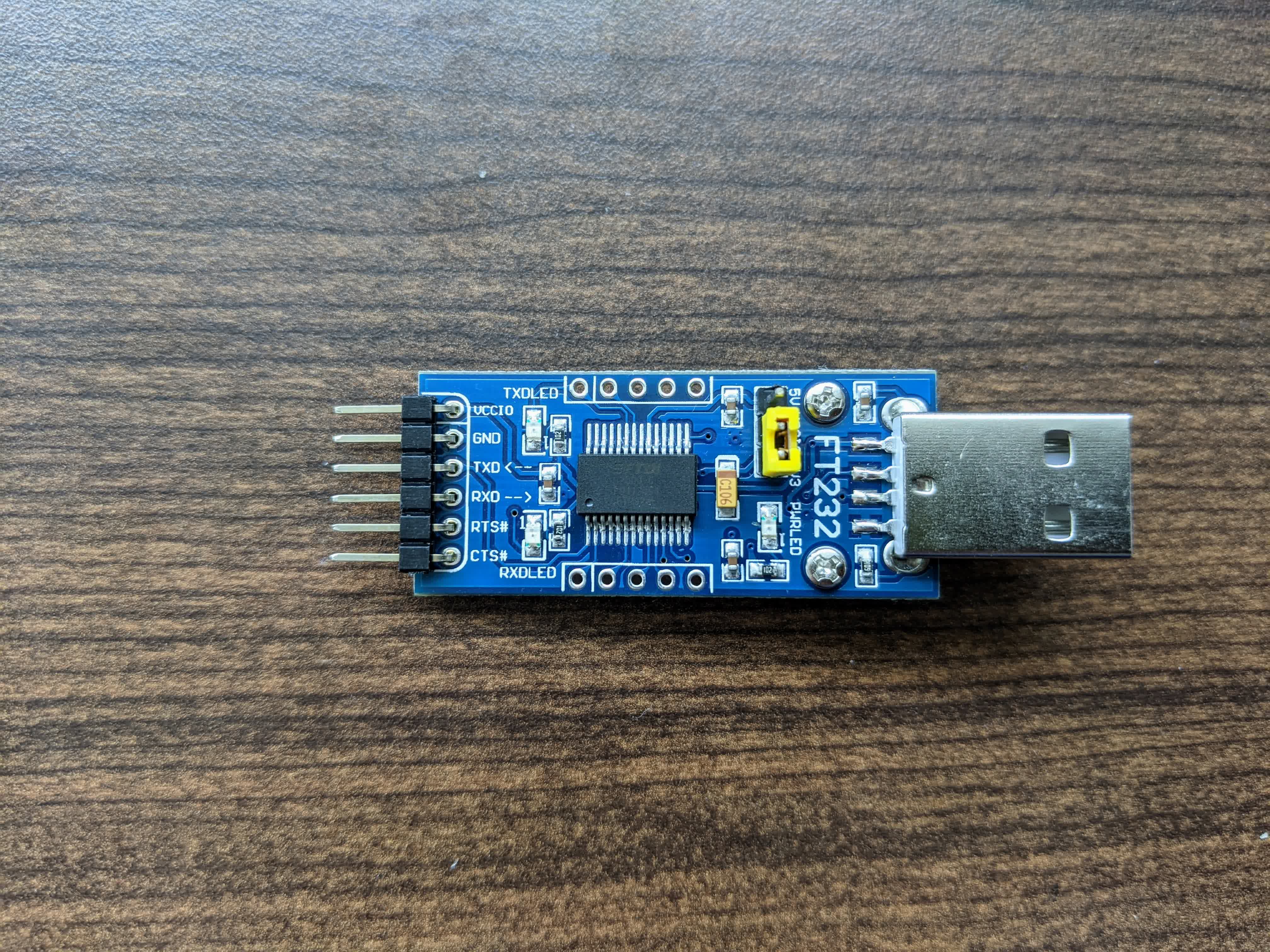
I know that I will be using the FT232 to connect to the PC, and jumper wires to connect it to my board's pins. However, the way I designed my board was exteremely inefficient. This is what I get for blindly following a tutorial without thinking ahead, but I was short on time, so whatever.
IF i wanted to make it work, I would have had to make an FTDI-UPDI serial adapter. This is shown below from the class website:
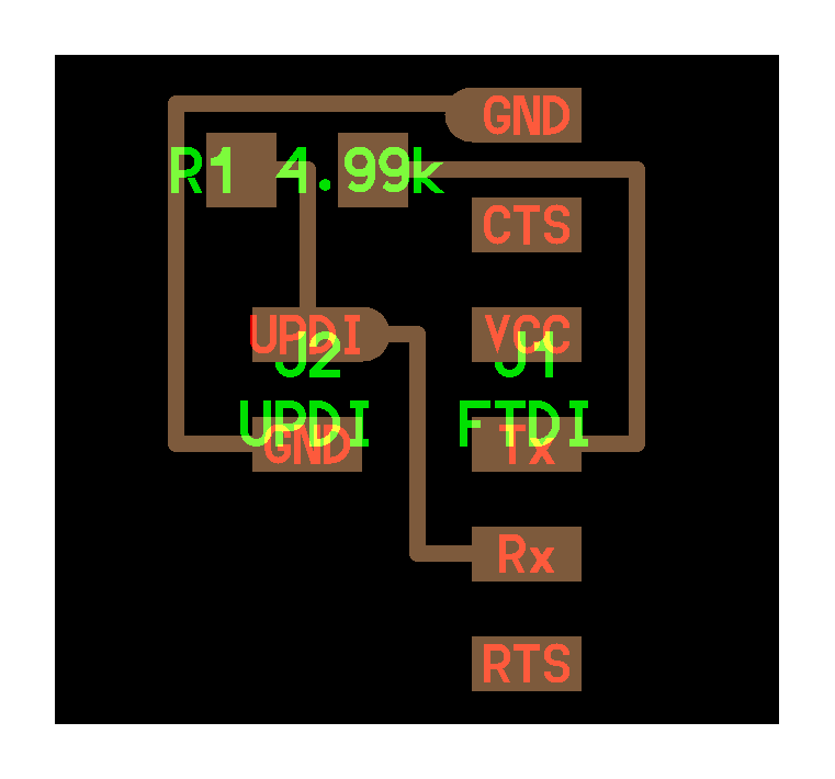
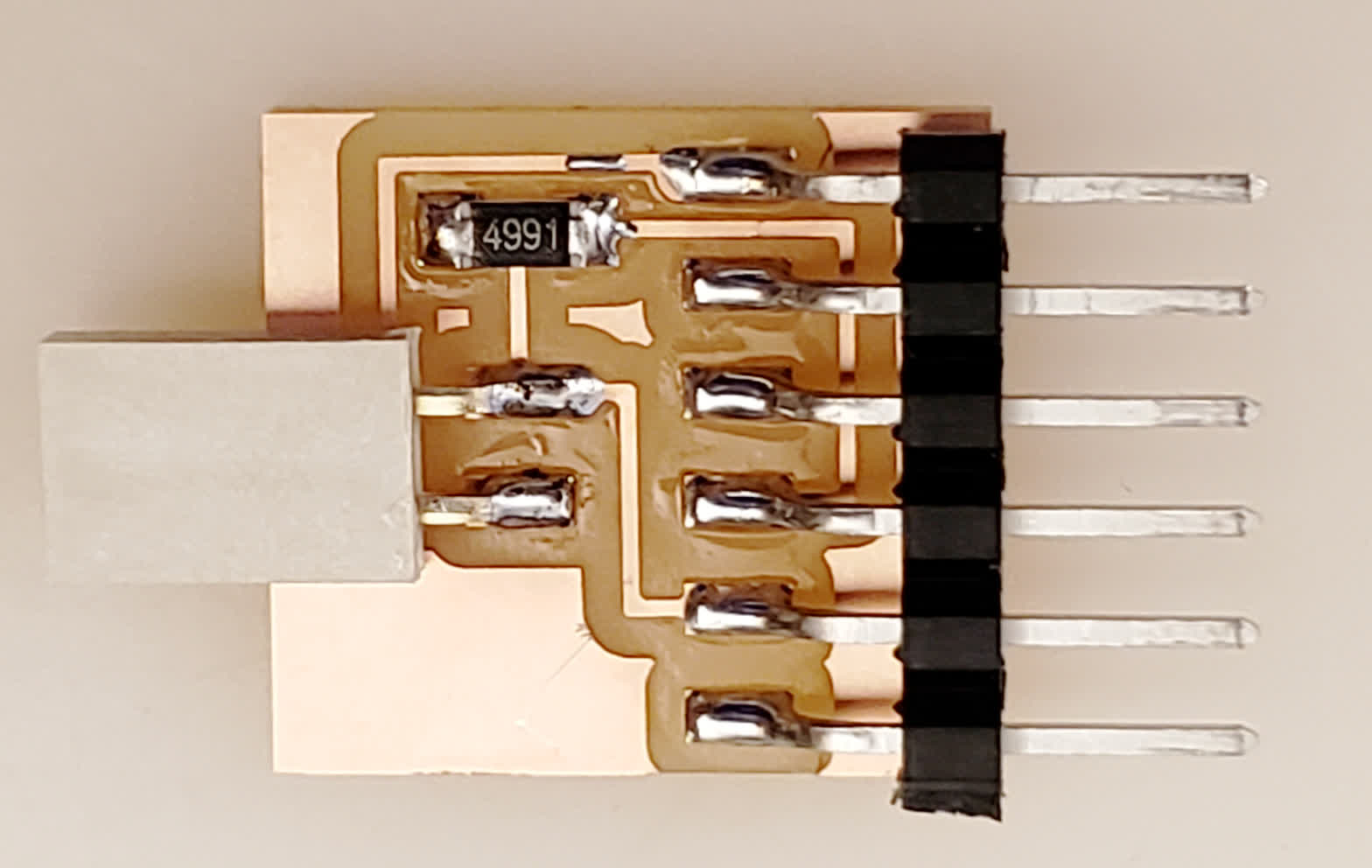
and here is what this adapter board would look like:
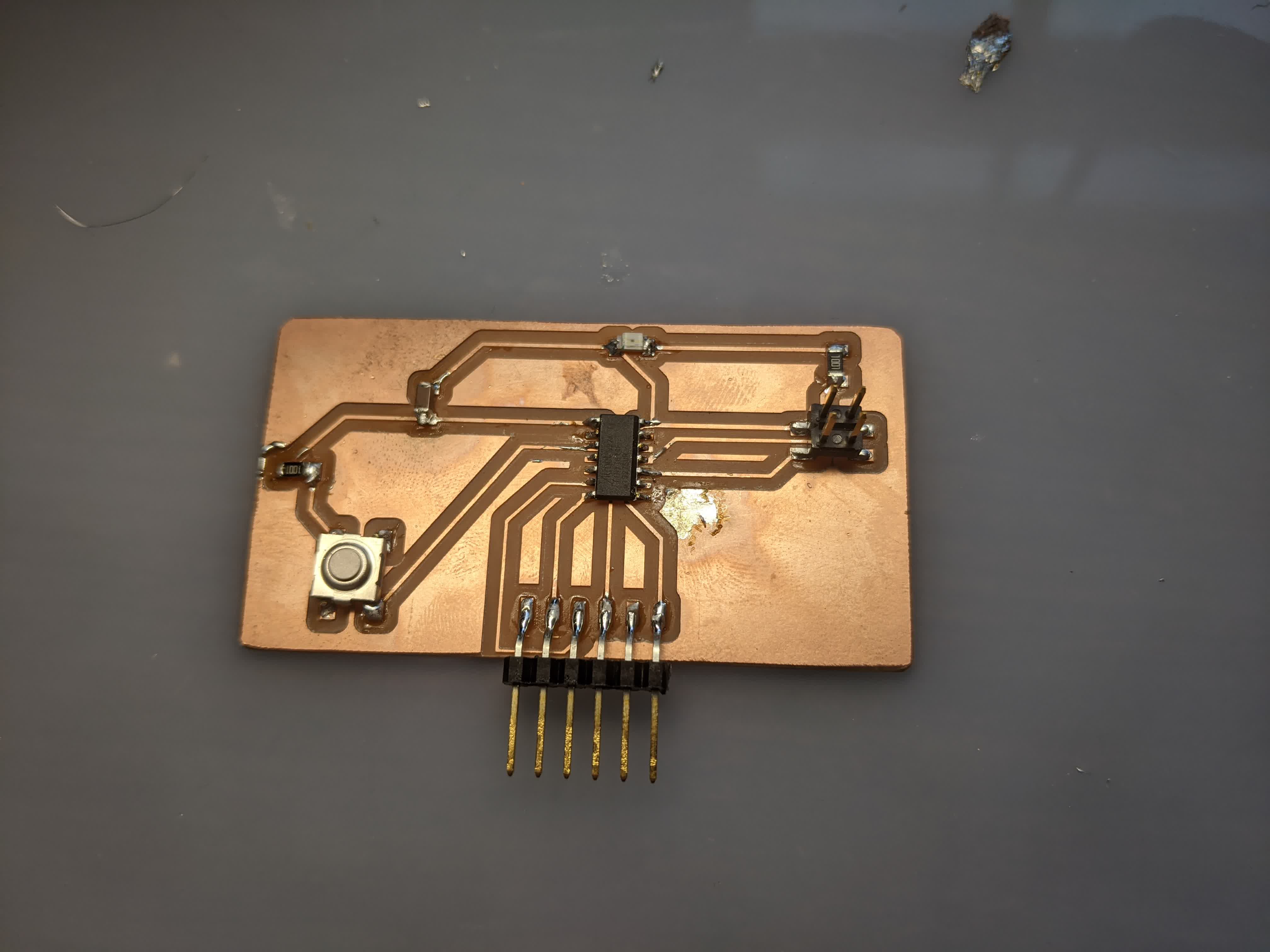
Here is my board from last week as a reminder:
Simply put, I would have to make the following connections:
-the VCC on the FT232 would connect to one of the pins on my board's 6 pin header (3rd pin from left)
-the GND on the FT232 would connect to one of the pins on my board's 6 pin header (6th pin from left)
-the TX on the FT232 would connect to the top female pin on the adapter
-the RX on the FT232 would connect to the bottom female pin on the adapter
-a single jumper wire would connect the 6 pin header on the adapter (third pin from bottom) to the bottom left pin of my 2x2 pin header to connect to the UPDI pin on the ATtiny1614
I learned that the advantage of the UPDI pin on the ATtiny1614 allows the chip to transmit and receieve data from a single pin. Here is a schematic of the chip which I pulled from the ATtiny1614's data sheet I reviewed:
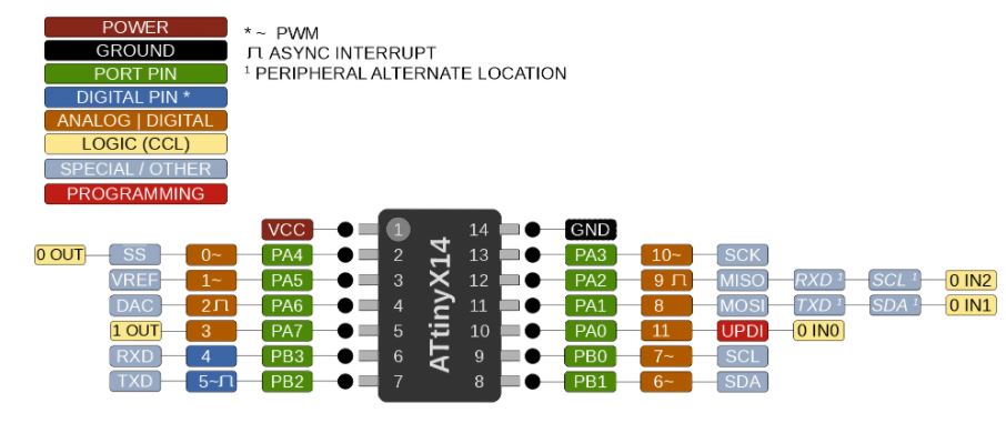
You can see here that the pin we would communicate with is Pin 10 (Port Pin PA0, Analog/Digital Pin 11). The whole purpose of the adapter shown above is to connect the transmitter line and receiver line to this one UPDI pin. There is a resistor on the TX line to allow the microprocessor to distinguish between data (ie voltage highs and lows that make up binary 1's and 0's) coming and going to/from the chip should there be data coming and going simultaneously.
I also learned that TX and RX are labeled from the perspective of the PC/programmer. TX drives the microprocessor (ie delivers data/code/commands to it), and RX is the data coming from the microprocessor. I think it's worth knowing this for programming purposes, however, UPDI technology makes it so that I, the programmer/designer, don't really have to know or make the distinction since they both go to the same pin, and the microprocessor differentiates between them under the hood.
I decided I would remake the board with the adapter built in to the design and only have pins that I need.
A huge thanks to Calvin who helped me understand all this!
Board redesign
This design was made with a lot more thought than last week where I blindly followed the tutorial.Pin Header
I know that from the FT232, I only need 4 pins: VCC, GND, TX, and RX. So I only need 4 pins coming out of my board. I decided to keep the 2x2 pin header in the original design and scrap the 6 pin header. The difference now is that before I was only using 2 of these pins, now I am using all 4. Here is the schematic of my redesigned board: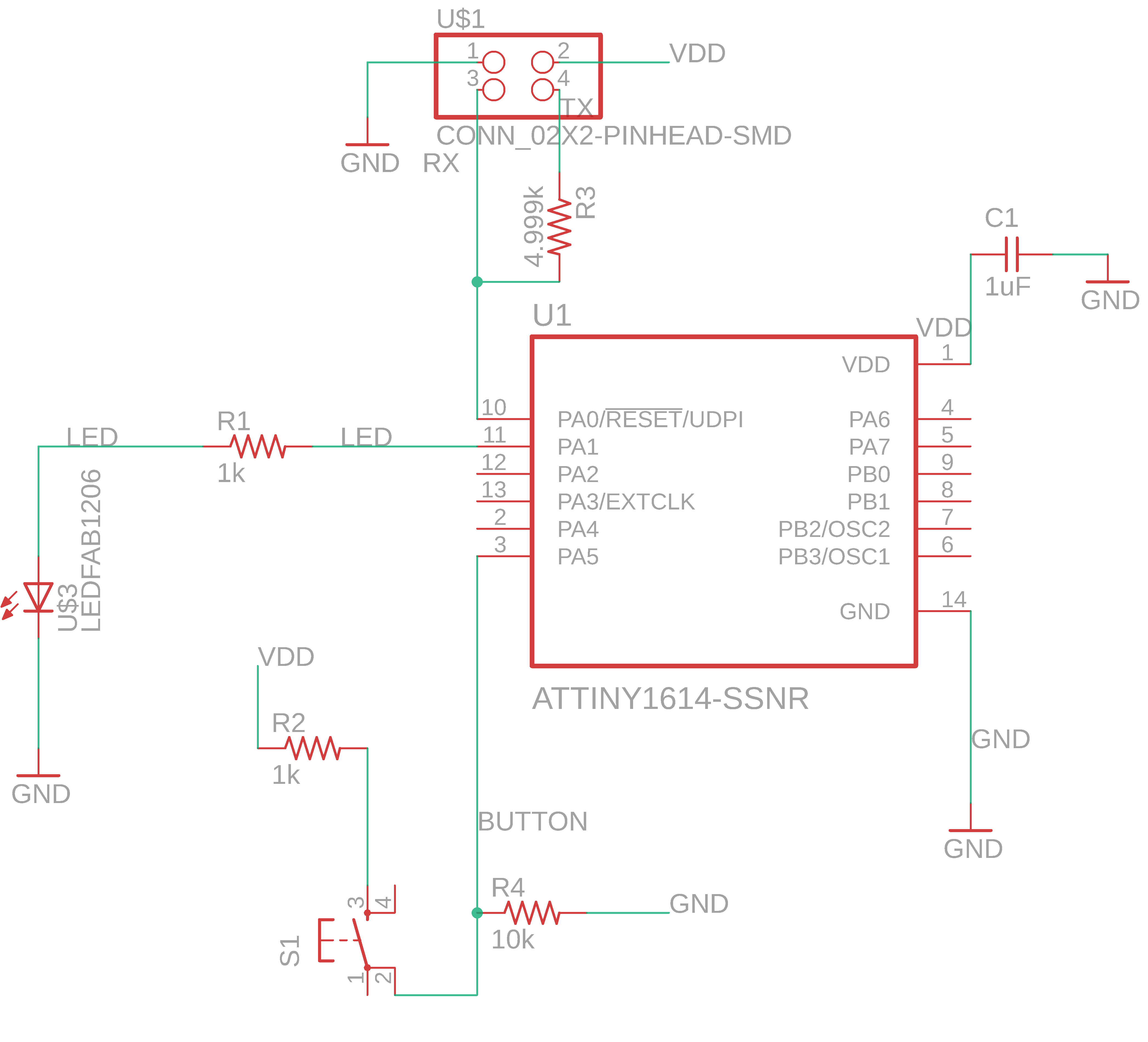
You can see now that the 2x2 pin header connects to the VCC pin of the microprocessor(Pin 1), GND on the microprocessor (Pin 14), and TX connects to RX with a 4.99k Ohm resistor who both then connect to the microprocessor's UPDI pin (Pin10).
Button System
I also made an additional change to my button system. You can see that I connected one leg to VCC (Pin 1) with a resistor connected in series to limit the current. I found out later that this resistor is extremely unnecessary and serves no real purpose, but it would be better to have it than not if it was the only resistor in this system. However, on the other leg of the switch, it is connected to the microprocessor on Pin 3, with a big resistor (schematic shows 10k Ohm, but I did not have 10k, so I put in a 47k Ohm resistor), which is connected to ground (Pin14). This resistor acts as a pull-down resistor ensuring the following:-with the button unpushed (open circuit), any noise or ambient charges or static build ups get pulled down through the resistor to ground
-with the button pushed (closed circuit), VCC will flow current through the button to Pin 3, and the big resistor blocks that current from flowing to ground
Now, with the button unpushed, Pin 3 will always read LOW, and with the button pushed, it will read HIGH.
LED System
No changes were made here, but I did learn a few things. I learned that we need the resistor on the positive leg of the LED to limit the current it is receiving. Without the resistor, the way an LED works (semi-conductor), it will build up current inifinitely and eventually burn out.I also learned how to test an LED. Using the multi-meter on the diode/connectivity setting, you place the black probe on the negative side and the red probe on the positive side. The LED will light up. This is a useful way to check the diode orientation before soldering it on the board as well as checking its color if you're clumsy like me and got a few of them mixed up.
Bypass Filter
The capacitor here is connected between VCC and GND to filter out any noise coming in to the microprocessor.This is the very simple redesigned board I made with a built in UPDI adapter, button, and LED.
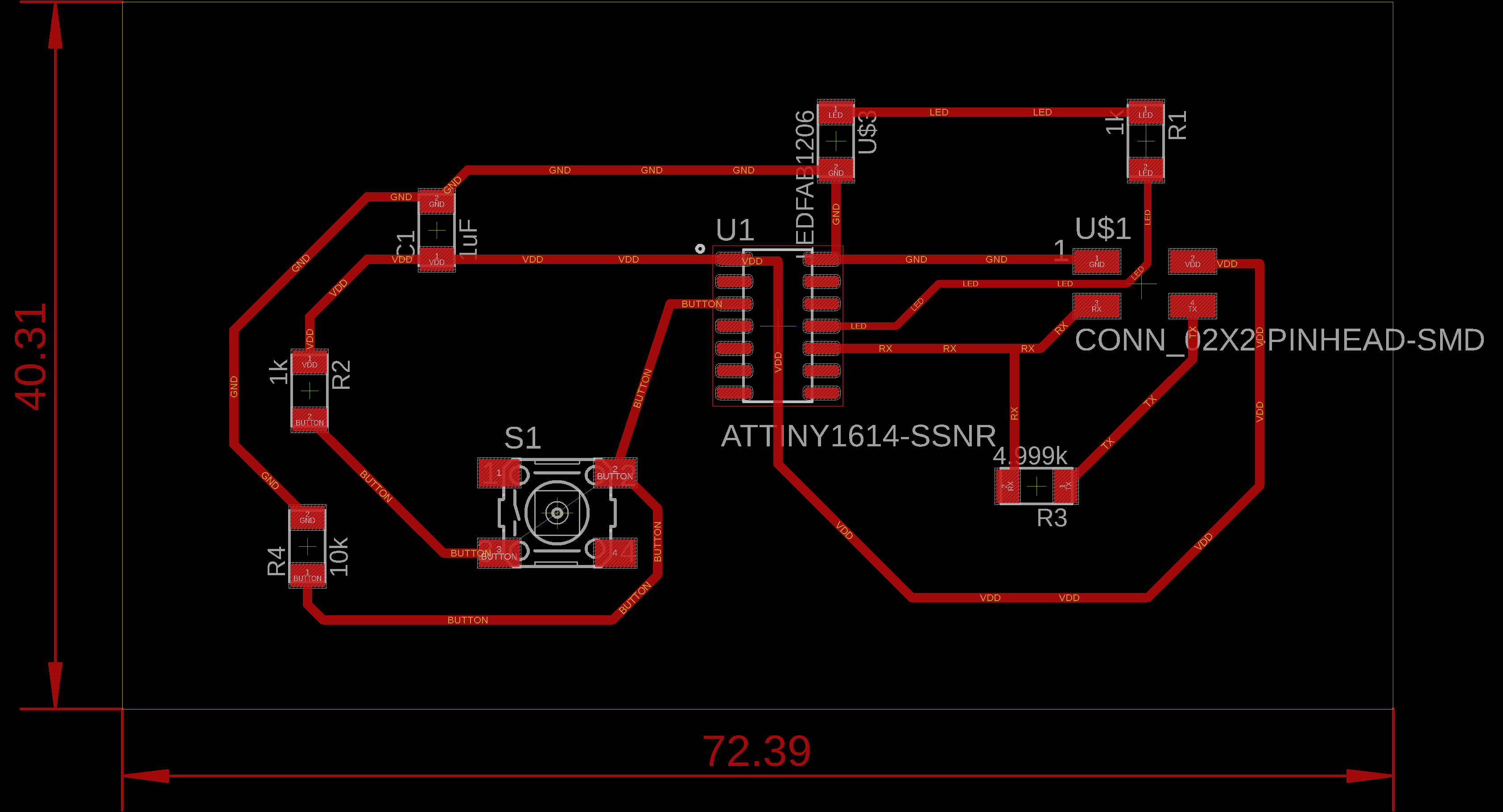
I remade the traces and here is how the board's footprint looks like now:
Exporting
The final step here is to export PNG's for toolpath planning. I learned about this very useful set of commands to be executed in Eagle's command prompt for quick and easy exporting:display none top to remove everything being displayed except the top layer (ie the layer of the traces I want to etch around)export image monochrome to export a black and white PNG and I set the resolution to 1000 dpidisplay none dim to only display the exterior dimention of the boardexport image monochrome to export black and white PNG (actually just exports a black rectangle) and I set the same resolution of 1000 dpi to ensure the cutout is to scaleI found that this is much quicker than exporting, then importing into Inkscape, and the drawing the cutout, then exporting 2 layers again.
Cutting
Here is the png of the traces exported from above: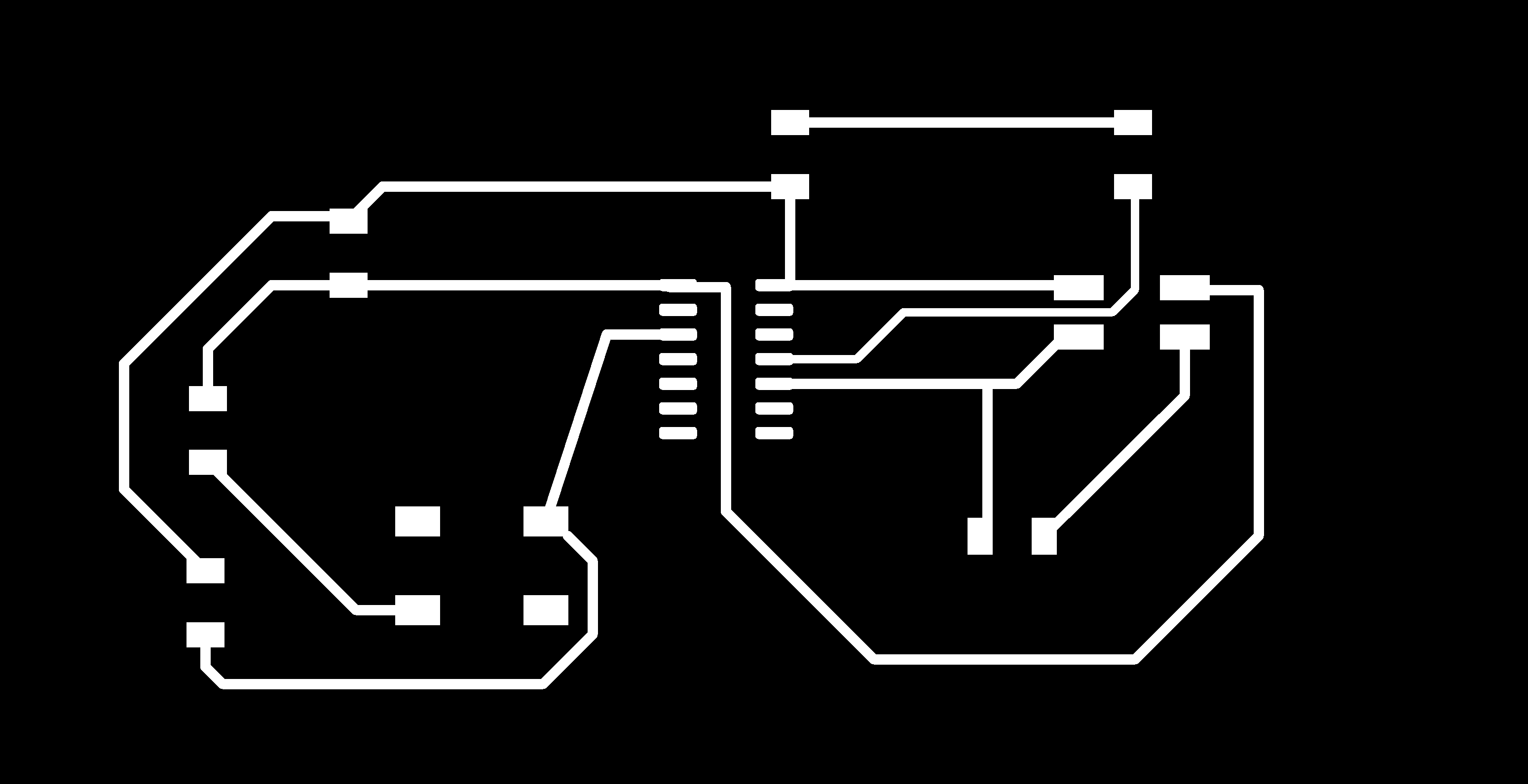
Here is the png of the cutout:

I take the two png's I created and put them into mods to generate the toolpath gcode.
For the traces, I used the following: tool diameter = 0.0156" (1/64", though I am using the V engraving bit), cut depth = 0.002", max depth = 0.008", offset = 6, cut speed = plunge speed = 1.5 mm/s
for the cutout, I used the following: tool diameter = 0.0312" (1/32"), cut depth = 0.01", max depth = 0.07", offset = 1, cut speed = plunge speed = 1.5 mm/s
Here is the toolpath for the traces:
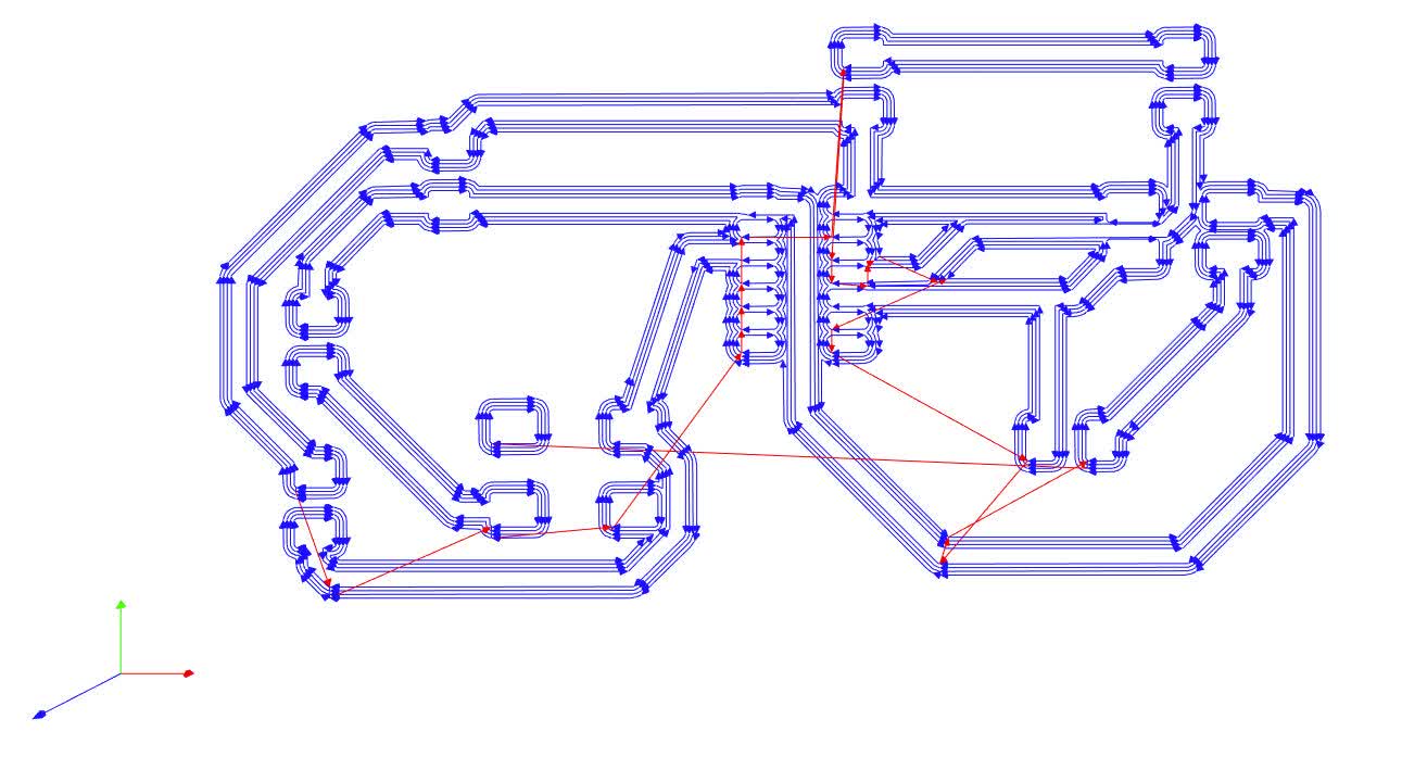
and the toolpath for the cutout:

I don't know why it has those additional unnecessary cutout on the right side, but I can live with that since it won't affect anything on the board.
Before cutting, I took a cheap toothbrush and some Gojo, and brushed the copper side of the board to make it clean for soldering later. I then wiped it down with alcohol along with the Clank bed to make sure it sticks without issues with the double sided tape.
Here is Clank etching aroung my traces like a CHAMP:
Even though I refaced my bed before doing this and shaved off an extra 0.005", it is apparent that my bed is not perfectly flat with respect to Clank's x-,y-, and z-axes. You can see the cuts are noticeably shallower on the left. Ultimately this doesn't matter because it it just the first pass, and I programmed in 4 passes.
Here it goes milling out the cutout around the board:
No issues here except the extra cuts on the right. It did cost me a bit of extra time, but I actually found it useful because it gave me some space to pry out the board after cutting was done.
Stuffing the PCB
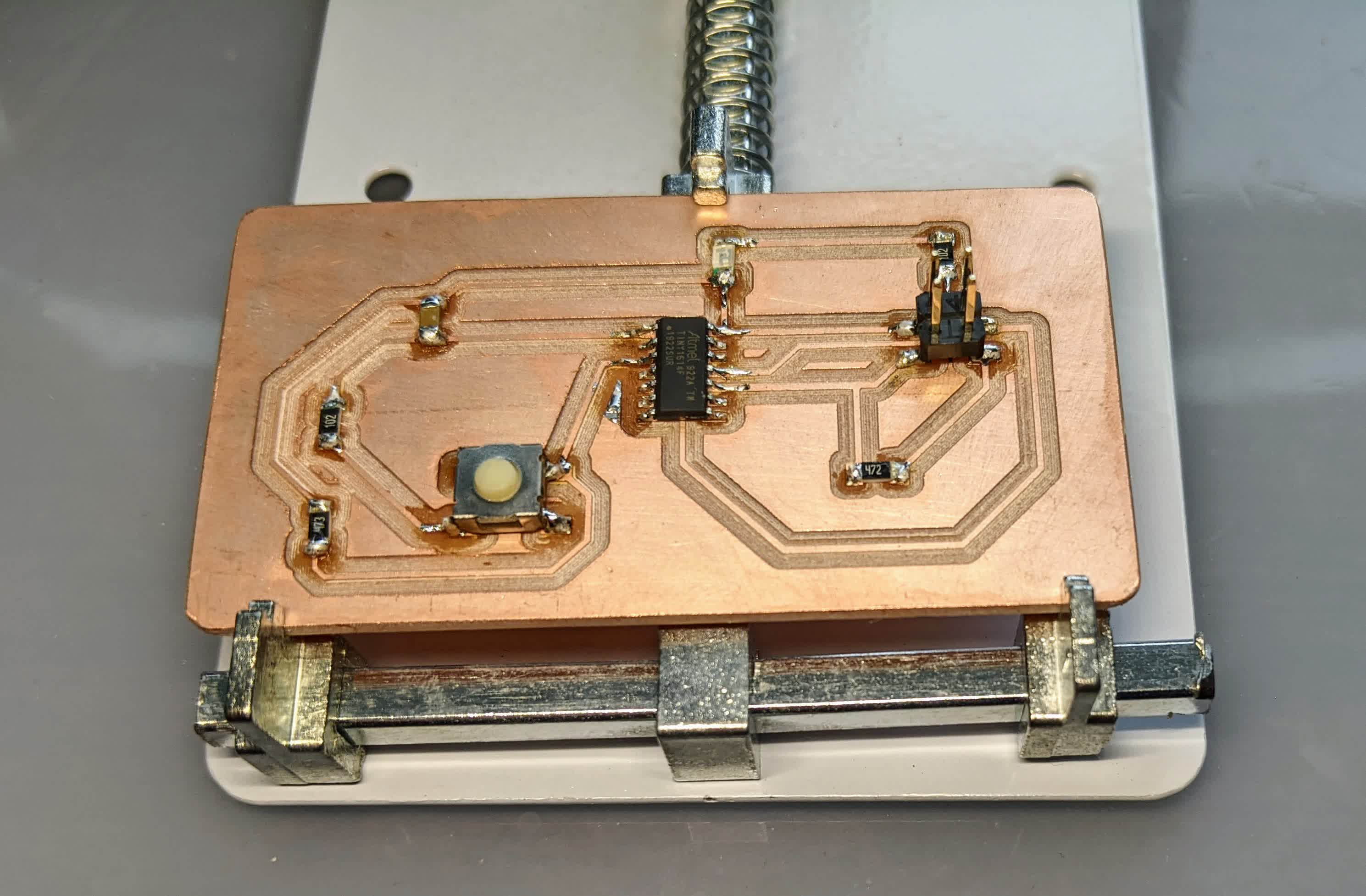
As always, I took out all the components and laid them out neatly before soldering.
I also got myself a cheap PCB holder to hold the PCB stready while I solder. I found it extremely frustrating to keep the hand holding the iron steady, the hand holding the tweesers holding the component steady, only to move the PCB as I solder. Here is my PCB held and ready to be soldered:
I also incorprated a new step to my work flow. I now put a dot of solder on the iron and simply touch a single pad of where the component will go. I do this for all the components before I put them on.
After that, I start with small components (resistors, capacitors, LED's, etc) and end with big ones (microprocessor, pin headers, etc). I follow the following procedure:
-put a dot of solder on the iron
-touch the iron to the leg of the component that I plan to solder to the board
-place the component exactly where I want it with the orientation I want (paying special care to press down after orienting on board) -touch the leg of the component which was previously soldered
-the solder will melt and flow, and melt the underlying solder on the board, fusing the component to the board (again, pay special attention to keep pressing down only without other movements)
-As soon as the underlying solder melts, immediately remove iron, but keep holding the component down for a few seconds to allow solder to harden
-for all other legs, simply touch the component leg with the iron to heat, and simultaneously touch with the solder to let it flow until you see the component leg and the underlying pad have been connected
I found this workflow to be very efficient and easy and takes less time for me. Here is the result:
Programming the Board to do Anything!
Given my recent experience with the FABTiny, I knew I would struggle. I had my PC ready and Raspberry Pi on standby in case I struggled with my Windows PC.Luckily, by the time I got here, Zach had posted this really awesome tutorial on how to get setup. This tutorial was extremely helpful for the ATtiny 1-series chips (412,1614,3216), and essentially sets up the Arduino IDE to code and communicate with our chips.
The first thing I did was setup the hardware. I used a USB extension cable from my PC to the FT232, and then 4 jumper wires onto the 2x2 pin header, routing each wire between the corresponding pins on the FT232 and my board as described above. This is shown here:

Setting Up
Before I get started here, I just wanted to give a huge thanks to Erik who helped me troubleshoot through this on both my Wondows and Linux machines!
This included the following setup steps:
Arduino setup
1-Download the Arduino IDE from their website.
2-Load the ATtiny cores by going to File-->Preferences, then pasting the following in the Additional Boards Manager URLS field: http://drazzy.com/package_drazzy.com_index.json
3-Go to Tools-->Boards-->Board Manager, and scroll all the way down and install the latest version of megaTinyCore by Spence Kode. Now the cores are installed.
4-Under Tools-->Chip:, be sure to select the microprocessor you are using. In my case, I am using the 1614.
5-Write your program in the Arduino IDE. You can open any example, I used File-->Examples-->01.Basics-->Blink. It really does not matter what you choose, we are only setting up now.
6-Go to File-->Preferences, and click on the preferences.txt to add the following line: build.path=C:\Users\Omar\Documents\Arduino\Hexes.
The idea is that you create a folder inside the Arduino folder (where all your coded sketches get saved) where the Arduino will store the .hex files every time a code is compiled.
I created a folder called Hexes in my Arduino folder, which will make it easy for me to go in there, copy the .hex file, and paste it in its respective sketch folder.
not Arduino setup
7-Install the latest version of python. You can do this by opening CMD on windows and typing: python, which will immediately launch the Microsoft Store and click on "Get" to download.
8-An optional step is to update pip3 to the latest version. Any time you use pip3 in CMD, it will direct you to the link to update.
9-Go to this repository and clone to your location of preference and extract the zip file. You can alternatively type :
pip install https://github.com/mraardvark/pyupdi/archive/master.zip in CMD to install, though this did not work for me. Maybe because I used pip, but should have used pip3 since
I installed python 3.8? In any case, you need to install pyupdi which is a python script that flashes your code onto your board.
Note: you need to know the exact path to pyupdi.py, and maybe copy the entire path down somewhere to make your life easier later.
10-In CMD, type: pip3 install intelhex pylint pyserial
11-Finally, in CMD, cd into the directory of the coded sketch that you wish to flash on to your board, then type:
python3 A -d B -c C -b 115200 -f D where
A is the full path to pyupdi.py, mine is C:\Users\Omar\Desktop\ClassRepo\pyupdi\updi\pyupdi.py
B is your chip name, mine is tiny1614
C is the port where you plugged in the FT232. You can find this in Arduino's IDE under Tools-->Port: and plug in the FT232 and unplug and see what appears. In my case, it is COM3
D is the name of your hex file
All together, you should have a command that looks like this: python3 C:\Users\Omar\Desktop\ClassRepo\pyupdi\updi\pyupdi.py -d tiny1614 -c /COM3 -b 115200 -f ButtonExcitingBlink.ino.hex
Hitting enter will load your program into your chip.
LED On/Off Program
The first thing I did was write a program that has the LED off by default, then on when the button is pushed. The important thing to note is calling pin names in Arduino is not
exactly calling the pin number. We have to refer to this schematic again:
My LED positive leg is connected to Pin 11 on the chip, which can be called using its port name PA1 (which can be a bit complicated to call) or by the brown/blue numbers, in this case 8.
Similarly, my button is connected to Pin 3 on the chip, so I call it using 1 in Arduino. Here is my code:
            /*

            LED Button

            This program turns the LED on when the button is pushed

            */

            int LED=8;int Button=1;int delay_Value=1000;

            // the setup function runs once when you press reset or power the board

            void setup() {

              // initialize digital pin LED_BUILTIN as an output.

              pinMode(LED, OUTPUT);pinMode(Button,INPUT);

            }


            // the loop function runs over and over again forever

            void loop() {

              int ButtonState=digitalRead(Button);

      if (ButtonState == HIGH) {

        digitalWrite(LED,HIGH);}

      else {

          digitalWrite(LED,LOW);}

        }
After writing this, I compile the code by clicking the verify (checkmark) button in the Arduino IDE. I then copy the .hex file from my Hexes folder into the folder containing the sketch.
Then I go into CMD and cd into the Arduino folder containing the sketch and input:
python3 C:\Users\Omar\Desktop\ClassRepo\pyupdi\updi\pyupdi.py -d tiny1614 -c /COM3 -b 115200 -f ButtonLEDOnOff.ino.hex -v
I found out that having the -v on the end makes it take longer to flash the code onto my board because it prints everything. So I removed that from future use for faster uploads.
Here is the result:
IT WORKS!!!
LED Slow to Fast Blinking
I could have ended it at that, but I wanted to do something a little more exciting. So I wrote a program that blinks the LED slowly by default (2s on / 2 sec off), but then blinks it fast when
the button is pushed (0.1s on / 0.1s off). Here is my code:
          /*

          Exciting LED Button

          This program blinks the LED every 2 seconds by default, but every 0.1s when button is pushed

          */


          //  Define variables

          int LED=8;int Button=1;int delay_Value=2000;


          //  the setup function runs once when you press reset or power the board

          void setup() {

            //  Initialize digital pins on ATtiny1614 according to pin schematic and if they serve as inputs or outputs.

            pinMode(LED, OUTPUT);pinMode(Button,INPUT);

          }


          // the loop function runs over and over again forever

          void loop() {

            // Have the default state of the LED blinking slowly

            digitalWrite(LED, HIGH);  // turn the LED on (HIGH is the voltage level)

            delay(delay_Value);       // wait for 2 seconds

            digitalWrite(LED, LOW);   // turn the LED off by making the voltage LOW

            delay(delay_Value);       // wait for 2 seconds

            //  Define state of button and assign the read value to it (pushed=HIGH, unpushed=LOW)

            int ButtonState=digitalRead(Button);

            //  Change blinking frequency if button is pushed

            if (ButtonState == HIGH) {

              delay_Value= 100;}

              else {

                delay_Value= 2000;}

              }
and here is the result:
IT STILL WORKS!!!
This is as exciting as it get for me with an LED and a button. Maybe a cool future project for me to do (idea courtesy of a conversation I had with
Gil) could be for the me to type something in, then have the LED
translate into Morse code. Again...till another day.
LED Button
This program turns the LED on when the button is pushed
*/
int LED=8;int Button=1;int delay_Value=1000;
// the setup function runs once when you press reset or power the board
void setup() {
// initialize digital pin LED_BUILTIN as an output.
pinMode(LED, OUTPUT);pinMode(Button,INPUT);
}
// the loop function runs over and over again forever
void loop() {
int ButtonState=digitalRead(Button);
if (ButtonState == HIGH) {
digitalWrite(LED,HIGH);}
else {
digitalWrite(LED,LOW);}
}
/*
Exciting LED Button
This program blinks the LED every 2 seconds by default, but every 0.1s when button is pushed
*/
// Define variables
int LED=8;int Button=1;int delay_Value=2000;
// the setup function runs once when you press reset or power the board
void setup() {
// Initialize digital pins on ATtiny1614 according to pin schematic and if they serve as inputs or outputs.
pinMode(LED, OUTPUT);pinMode(Button,INPUT);
}
// the loop function runs over and over again forever
void loop() {
// Have the default state of the LED blinking slowly
digitalWrite(LED, HIGH); // turn the LED on (HIGH is the voltage level)
delay(delay_Value); // wait for 2 seconds
digitalWrite(LED, LOW); // turn the LED off by making the voltage LOW
delay(delay_Value); // wait for 2 seconds
// Define state of button and assign the read value to it (pushed=HIGH, unpushed=LOW)
int ButtonState=digitalRead(Button);
// Change blinking frequency if button is pushed
if (ButtonState == HIGH) {
delay_Value= 100;}
else {
delay_Value= 2000;}
}
Files:
Traces gcode
Cutout gcode