Week 04: ELECTRONICS DESIGN
A. BOARD DESIGN
A1. Eagle set-up
1.1 To to all of my designing in Eagle I followed this tutorial. I've never worked with electronics before, so am very very beginner. This tutorial was very helpful in walking through every step.
Tutorial Link: http://mtm.cba.mit.edu/2021/2021-10_htmaa-demo/
1.2 First you need to set up your fab libraries in Eagle so that you can add the specific fab lab components to your design. Download the fab.dru and fab.lbr files here. Then go into Eagle in the board window and click file > new electronics design > create > new schematic > switch > PCB document, then type drc in the command line. This should open a window and on the first tab click load > fab.dru. Now your libraries should be loaded! You can go to the library settings and click the fab library to "in use" so it is easily accessible while designing.
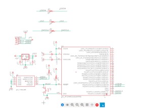
A2. Schematic design
2.1 I followed the tutorial to learn the basic Eagle commands; how to add components "add", add component names "name", connect components "net", move components "move", and rotate "rotate".
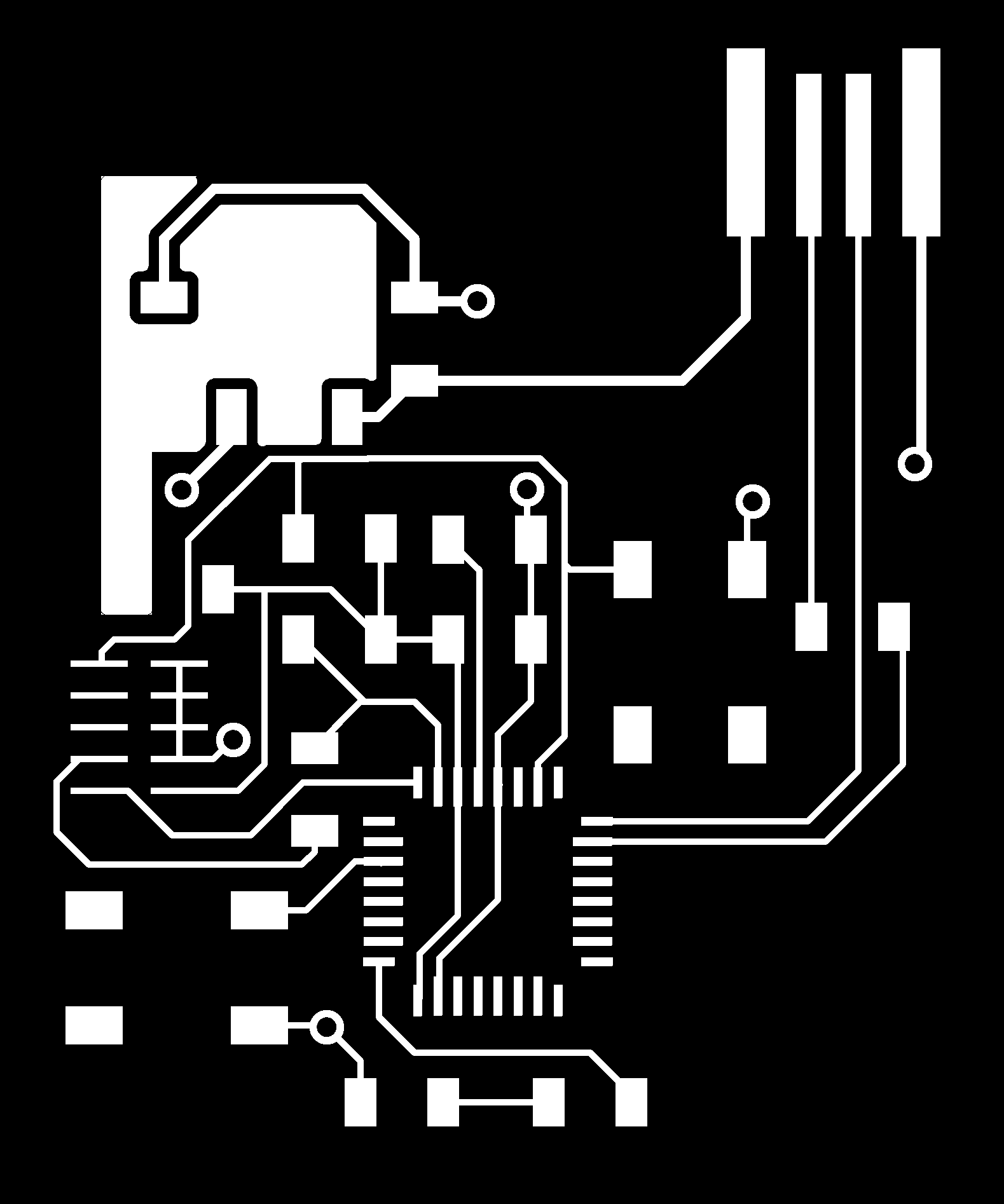
2.2 Using all of these commands I added my components to the board, following the tutorial, and connected them to each other until my schematic looked like the photo above.
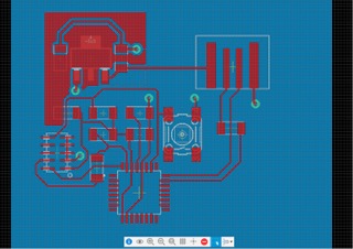
A3. Board design
3.1 After setting up all my components in the schematic I then switched to board view to start the physical design and routing of my board.
3.2 I used the commands "route" to place copper traces, "rip up" to remove them, "move" to move my components, and "drc" to check for errors on my board
3.3 First, you have to lay our your components. I followed the tutorial and put my components in similar places.
3.4 Then you can start routing your wires, again I followed the tutorial for this because it was very new to me. But you want to connect all of your pieces following the yellow "airwires."
3.5 If you run into issues with wires needed to intersect you can add a 0 resistor to jump other wires. Go back to your schematic and add a resistor w 0 ohms and connect it to two of the same wires of the wire you need to jump with.
3.6 In this tutorial they used vias to connect the grounds to the back of the board (I actually didn't realize this until milling my board out of one sided copper and then finded out what a via actually was). Basically it makes your routing easier because you can just connect the ground pins to a via instead of jumping over all the other traces.

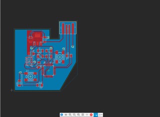
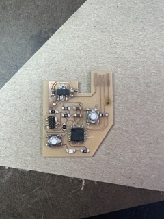
A4. Adding LED + button
4.1 So after milling my board on the wrong material, I also realized I didn't add an LED and a button because I assumed the tutorial has everything and didn't realize it didn't include an LED and button.
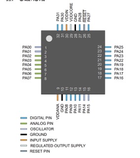
4.2 So I went back into my schematic and added and LED connected to one of the pins of the microcontroller (found right pin from datasheet online of my SAMDE18A microcontroller). The other side of the LED was connected to ground.
4.3 Then I added a switch connected to a resistor and the LED and ground. For this I followed the EECS TA's advice on how to add the LED and size the resistor to 500 ohms.
4.4 Then I re-exported my new board.
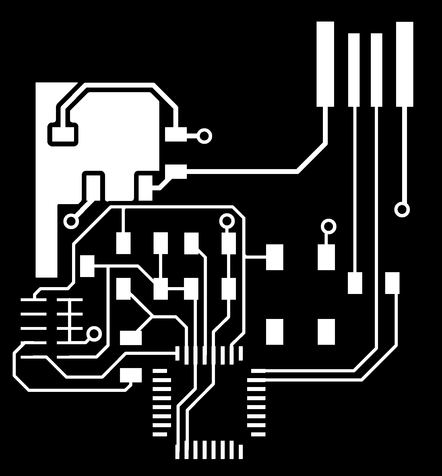
A5. Exporting PNGs
5.1 To export your board you go to your board design file and type "display mode top dimension vias" and "export image." In the export image box press monochrome and 1000 dpi then export. These are your traces.
5. 2 To export your outline and vias type "display mode bottom dimension vias." Export with the same settings as in 5.1.
5.3 Then you have to bring the files into photoshop to clean them up and seperate the outline + vias file into seperate files. The vias are milled with the 1/64 mill bit but drill all the way through the board so they have to be exported as a seperate file.
B. BOARD FABRICATION
B1. Milling
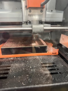
1.1 I followed the same milling steps I detailed in week 2.
1.2 First I set up the Roland Mill machine, attached my copper plate, and set the origin of the mill bit.
1.3 Then I uploaded my trace jpg and made sure it was the same size as the photoshop files.
1.4 I sent the trace to cut with the 1/64 mill bit
1.5 Then I uploaded the vias file and changed the mods settings to be mill outline, and made sure to change the diameter to 1/64 (you have to put it as decimal into mods).
1.6 Then I changed the mill bit to 1/32, changed the tool diameter in mods back to 1/32 and cut the outline.
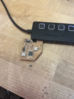
B2. Soldering
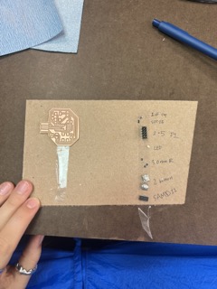
2.1 Had the archshop TA help me with finding the pieces this time so I could start to understand what was going on my board. It was actually a lot easier now that I had the eagle file and could see the names of the components I used, and then just looked for those in the many many drawers.
2.2 After collecting my components I started soldering them all on.
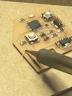
2.3 To solder the vias I had to use a piece of wire and string it through the via hole and then solder it to both sides of the board
C. BOARD PROGRAMMING
C1. Use programmer to add software to board
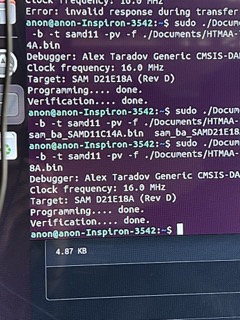
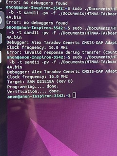
1.1 Luckily I had a lot of help from my TA for this. Since my bootloader from week 2 didn't work as a result of my beginner soldering, I had to use the etmel programmer in the shop to program my board.
1.2 First you download the binary code from the HTMAA website for your specific microcontroller. Mine is the SAMD21E18A. Then navigate to the edbg file to flash code onto your microcontroller.
1.3 Then you connect your board to a USB port thats connected to the computer and then connect your board to the bootloader with the pins. My board didn't fit into the USB at first because of its geometry so I had to sand it down a little.
1.4 I connected my board and my TA's bootloader recognized it, yay!! success!! woohoo!!!!! This was very exciting, first time I had a partially working board. This also means that my board should be able to be programmed through USB by my computer.
C2. Use USB to program functions on board
2.1 Next, my TA showed me how to open Arduino to put a program on the board. Unfortunately Arduino did not recognize my board so I went through a very long debugging process.
D. BOARD DEBUGGING
D1. Although I could bootload my board, Arduino didn’t recognize it so I couldn’t program it. I did a lot of debugging using the multimeter and re-soldering connection points. I even connected my voltage regulator with a wire to ensure a strong connected but it still didn’t work. At this point the class had moved on to the next week so I decided to come back to my board in week 6 when we started with programming again.
D2. Successes this week included designing my board in eagle, which I had never used before! Also finding all of the components because that was something I was completely clueless in week 2. Lastly, learning how to solder the vias and wire to connect ripped up traces or pins was also fun and made me more confident in my soldering skills.
E. WORKING BOARDS...
As an electronics beginner it actually took me until halfway through the sixth week to get a fully working board. This page documents the basics for electronics design but to see the documentation for a fully working board skip to my week 6 page where I go through the process of designing and successfully fabricating two more boards.