This week, my journey through the world of electronics and circuit design led me to the exciting realm of PCB design. Armed with the Xiao Development Board and two powerful design tools, Kicad and Eagle (Fusion 360), I embarked on a mission to create innovative development boards that combine form and function. In this post, I’ll share my experiences and discoveries, offering insights into the process and some valuable takeaways.
Designing with Kicad:

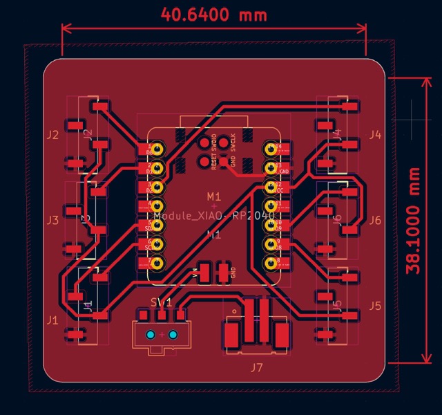
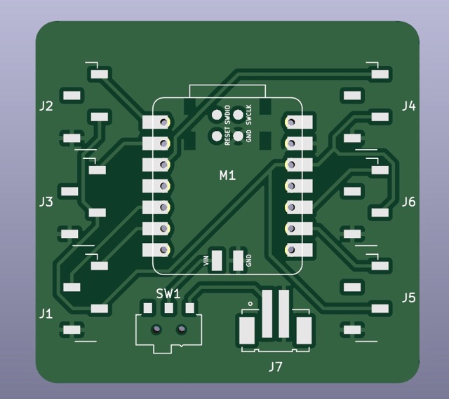
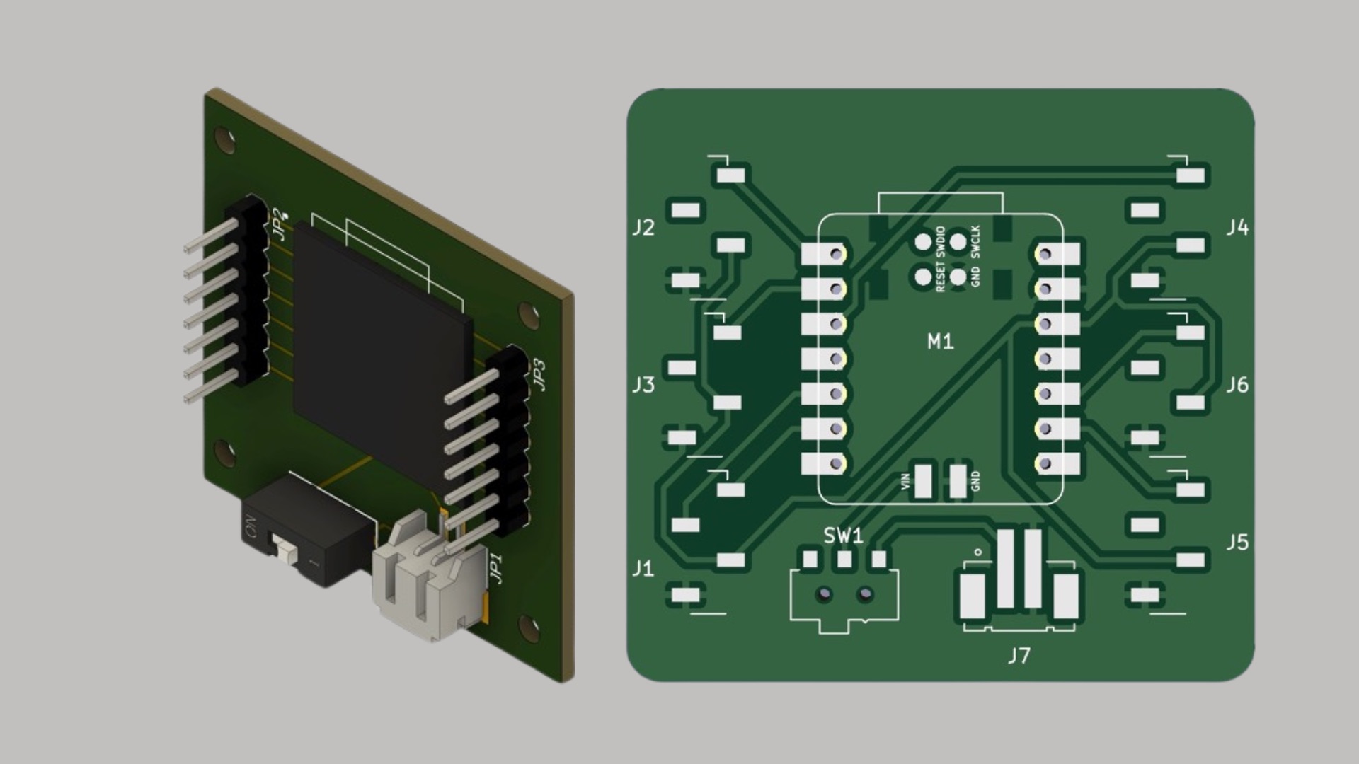
My adventure began with Kicad, a popular open-source PCB design tool. My primary goal was to create a Xiao development board, equipped with four standard Grove connectors, an I2C connector, a JST LiPo battery female socket, and a power switch. Kicad provided the ideal platform for designing a feature-rich development board. I carefully mapped out my components and interconnections, ensuring a neat and efficient design. An exciting feature I explored was the “pour copper” function, which allowed me to establish a common ground throughout the board, optimizing connectivity and performance.
Going the Extra Mile with Eagle:
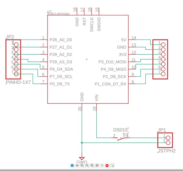

To challenge myself further and gain a broader perspective on PCB design, I delved into Eagle. With this tool, I designed another Xiao development board that featured two 7-pin headers, a JST LiPo battery female socket, and a power switch. Eagle’s interface and functionalities offered a distinct experience, broadening my skillset. This dual approach allowed me to gain proficiency in different design environments and identify the strengths and weaknesses of each tool.
Bringing It to Life with Fusion 360:
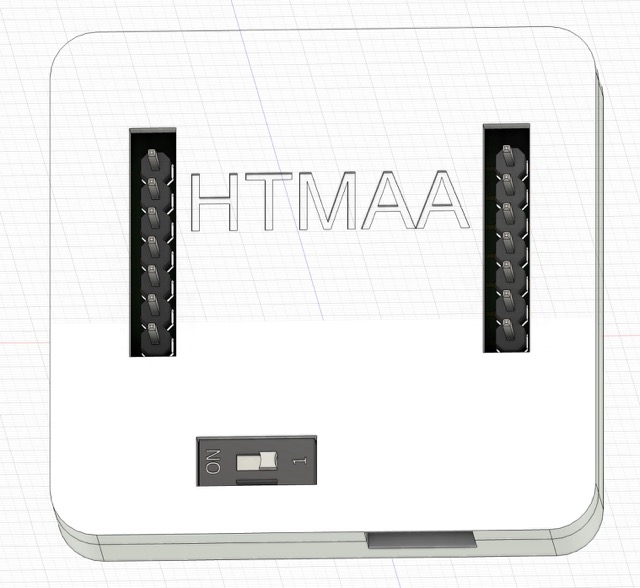
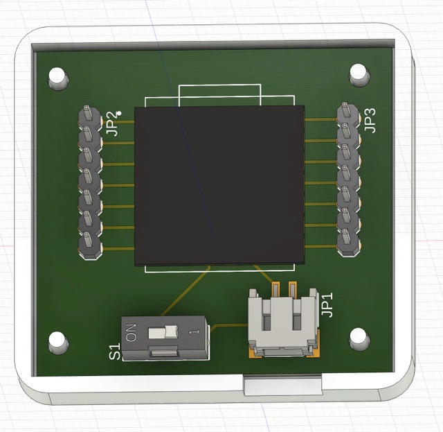
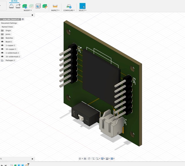
One of the most exciting aspects of my project was the ability to integrate my PCB designs into Fusion 360. With Fusion 360’s capabilities for 3D modeling, I was able to create custom enclosures for my Xiao development boards, ensuring they were not only functional but also aesthetically pleasing. The fusion of electronics and 3D modeling opened up new opportunities for creativity, enabling me to design cases that matched my boards’ form and function.
Challenges and Takeaways:
While my journey was filled with success and innovation, it was not without its challenges. Fusion 360’s operational logic, though powerful, required me to adapt my approach, especially if I was accustomed to working with software like Solidworks. However, this learning curve also meant I expanded my skillset, making me a more versatile designer.
This week of circuit design with Kicad and Eagle (Fusion 360) was an enriching experience. I honed my PCB design skills, experimented with different design environments, and discovered the limitless potential of combining electronics and 3D modeling. This exploration has opened new doors for innovation, and I look forward to applying these newfound skills in future projects.
Stay tuned for more exciting developments on the How To Make Almost Anything website as I continue to explore the endless possibilities of creation and innovation. Join me on this exciting journey into the world of circuit design and beyond!
Design rule
TODO
- https://docs.oshpark.com/design-tools/kicad/kicad-design-rules/
- File -> Board Setup -> Constrain
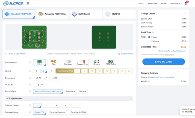
Order PCB