Week 15 - Final Project Presentations
This week we presented our final projects to the rest of the class and had an open house where friends of the program could come by and see what everyone made!
Assignments:- Prepare a summary slide for your final project (optional)
- Prepare a video on your final project (optional)
Optional Assignments
Both the assignments this week are technically optional as the final project page contains a lot of the documentation for what we did this semester even though we are encouraged to make them. I definitely don't have very good video editing skills, but I did make a summary slide which can be seen below!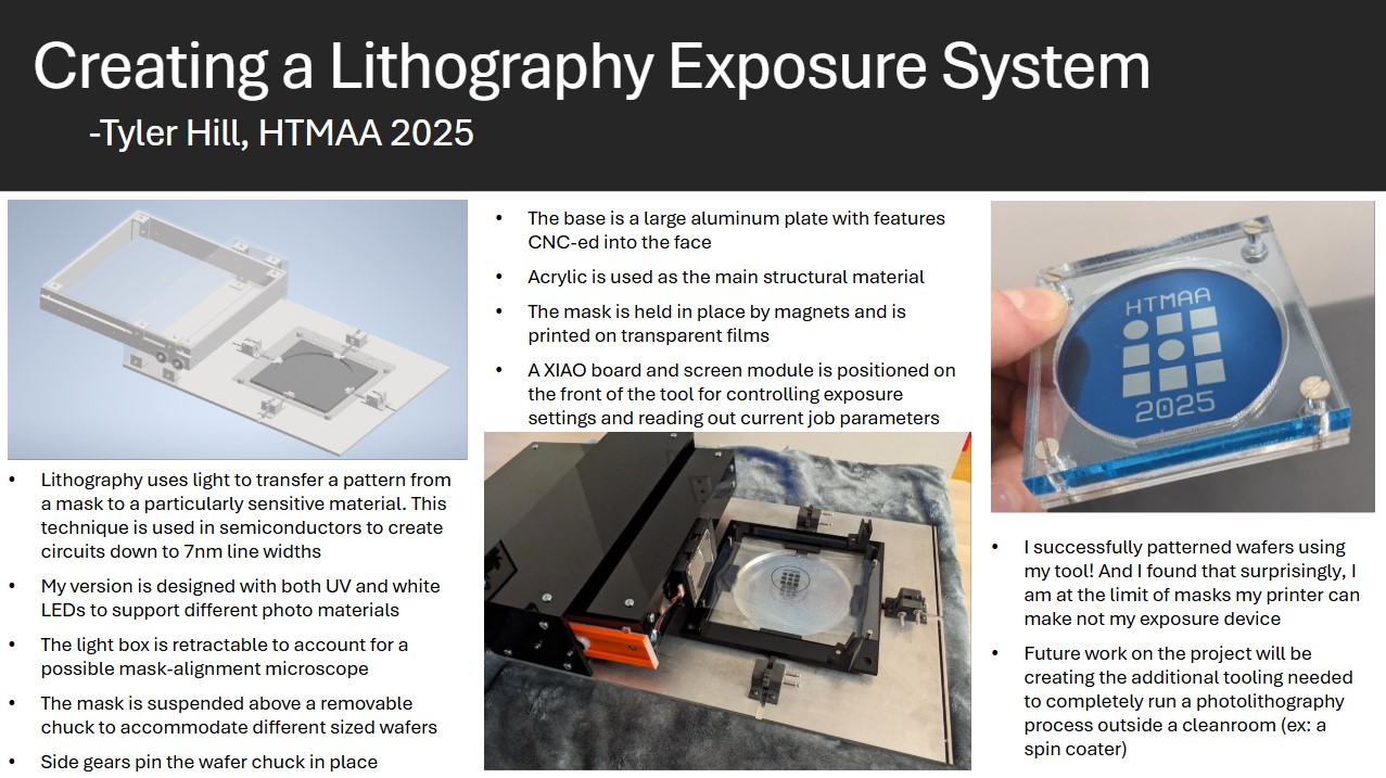 PDF Download
Final Project Questions
What does it do?My final project is a photolithography exposure tool. It takes in a photoresist coated wafer and a mask, it helps the user align them to print the pattern properly, and it exposes the wafer with parameters determined by the user. The user can select from UV and white light exposure sources, they can set the exposure time, and they can set the power level of the light source.
Who's done what beforehand?
There are a lot of companies that do photolithography very well. ASML is the world leading tool manufacturer that can reliably make features down to and maybe even surpassing 7nm. They make tools that contain the optics, light sources, projection/scanning capabilities but a user will still need to purchase masks usually from different vendors that are then made to work with certain tools. There are also a number of direct-write lithography systems which offer the advantage of being maskless, meaning they are better for R&D environments where designs are still changing but they take a while to run. The ones I have used personally are made by Heidelberg (.nano has at least one of their tools, maybe more). When it comes to homemade lithography systems, it is generally common knowledge that crude masks can be made by printing a design onto a transparent film, and shining light through that film. This process is called shadow masking, and it won't produce super precise devices but it is a very quick and cheap technique when those are limiting factors.
What sources did you use?
I really didn't use many online resources outside of the ones I documented for their various uses (the one that comes to mind is the feeds and speeds wizard for CNCing my metal parts). I read a lot of data sheets to make sure I was using the right parts based on their capabilities, but that didn't really help me develop my idea. One site I did look through, was a forum post here discussing how to make light more parallel. They suggested using a privacy filter to narrow the angle of transmitted light, but I ended up not using this in favor of doing contact-masking.
What did you design?
I made nearly all of the components that went into my final project. I designed all of the structural acrylic/metal components, all of the 3D printed parts (both on the MK4S and Fuse 1+ SLS), and all of the electronics boards that controlled my system. I also designed all of my testing files such as the GDS files that then became the masks printed on transparency film.
What materials and components were used?
Most of my structural components are made out of acrylic, but the base plate (and wafer chuck) is made out of aluminum to make sure the system stays flat. I made use of both PLA and PETG for traditional 3D printing, but I also used nylon from the Fuse SLS system for a large portion of my printed parts. On the electronics side I used the copper on FR1 stock to mill my boards which were populated with an ESP32C3 XIAO, a TFT screen, a USB-C power breakout board, various resistors and capacitors depending on the use cases, MOSFETs (SI2336DS-T1-GE3), white LEDs (QBLP650-IW), UV LEDs, and various pin headers/female connectors. The light board did also have a 5V regulator and diodes to prevent reverse biasing the power supply, but for my final use case I bypassed these components (more details can be found in the electronics section). For general hardware I used ball bearings, pinions, magnets, and various sizes of screws and nuts. Most were likely made of steel, but I did use a couple of nylon standoffs for one of my PCBs. Lastly, I used transparent paper and vellum paper for my photomasks.
Where did they come from?
Almost all of my acrylic and metal stock I was able to source from the Hobby Shop scrap pile since I am a member there. The exception is the large aluminum piece I used as my base, but Dan came in clutch here because he was getting ready to get rid of an old system of some kind and let me take the piece I needed. I did order the transparent and vellum papers from amazon, along with the magnets, ball bearings, and UV LEDs. Otherwise, all the other components I used (screws, electronics, printing materials, etc) were sourced from the class inventory or the supply bins in the CBA shop.
How much did they cost?
The amazon orders were $6.99 for 30 sheets of transparency paper, $7.99 for 50 sheets of vellum paper, $14.88 for 60 pieces of the magnets, $12.99 for 20 UV LEDs, and $6.99 for 20 of the ball bearings. I did not have to pay for any stock that I used but based on the available material from McMaster, I would have had to get a 24" x 24" in 1/4in thick plate for ~$130 and my acrylic would have been something like $50 for each 1/4in plate of 24" x 24". So maybe the total acrylic cost would have been on the order of $100, possibly closer to $150 if I wanted to get an additional smaller plates as a backup for cutting parts.
When it comes to the shop inventory, the PLA filament is listed at $57 but PETG and the nylon powder is not listed. I definitely did not use a whole spool of filament, or even close to a whole case of nylon powder, so it is hard to estimate what my printing costs came out to be. On the electronics side, my XIAO was $4.99, the USB-C power board comes in a pack of 12 so each board is about $2, the voltage regulator that I ended up bypassing was $1, the TFT screen was $12, the PCB stock itself was about $2 per board, and all the remaining components were single-digit cents so I can approximately say $5 would cover all my LEDs, resistors, capacitors, pin headers, and connectors. That brings my total project cost (including a whole filament spool but excluding any of the tooling required) would be around $414 with the large part of that cost being $280 towards stock. All the individual components that went into the project make up less than $100.
What parts and systems were made?
Aside from the components that I listed above, I made/cut/programmed everything. This included the gear system and linear rail that would align the wafer chuck, The mounting mechanism for the mask frame, the light box rail system that allowed it to extend and retrace, and the brackets that held the entire system together. In the code I made use of existing packages like Flat UI, WebSerial, and a TFT library for drawing shapes and text on the screen. But past those libraries I designed the communication hooks between the XIAO and the web interface, I made what is essentially a state machine for exposing the substrate, and I made the simple TFT UI that just shows the parameters currently being used for the exposure.
What tools and processes were used?
I did a lot of laser cutting on the XTool P2 and the Epilog to shape all of my acrylic. I use the water jet in the CBA shop to cut my aluminum parts to size and the Haas Super Mini Mill at the hobby shop to CNC the surface patterns of them. I made use of the Prusa MK4S's and the Prusa XL 3D printers to make all my PLA and PETG parts, along with the Fuse 1+ 30W SLS printer to make my nylon parts. The nylon printing process also used the Fuse Sift to reclaim some of the un-sintered nylon powder, followed by glass bead blasting to completely remove any loose material without damaging the parts. Parts were finished by using drill presses in the CBA and Hobby shops, or with hand tools found in both locations such as files, sanders, and taps.
On the electronics side, the Carvera was used to mill PCBs with a 1/32in endmill to cut board footprints and vias and a 1/64in endmill to cut the traces on the surface. We then used soldering stations equipped with flux, tip tinner, wicks, lead-free solder, and hot air guns to solder all of the necessary components. I tested my light board with the power supply and oscilloscope found in the electronics bay. When it came to testing my project, I made use of a cleanroom spin coater and hot plate to coat and bake my wafer prior to exposing it on my tool that I made. I printed the masks used in the exposure on an old ink jet printer.
I did all of my physical CAD in Autodesk Inventor and imported the designs into Fusion 360 to handle the CAM-ing process. I also did all of my PCBs in the Fusion PCB editing software. All of my microcontroller code was written in the Arduino IDE, and my local HTML WebSerial interface was written in the Cursor IDE using examples I found online as templates.
What questions were answered?
Well, the main question I answered was can I do lithography and the answer is a yes with a slight asterisk! I did need supporting equipment to complete the entire process which I hope to also make versions of, so I am technically part of the way to making a photolithography process I can do outside a cleanroom. I was a little worried that my LEDs would not be the advertised wavelength because they were cheap and I got them on Amazon, but my resist developed so they were at least in the right wavelength range and that is good enough for me. Other than that I don't think there were a lot of questions I was unsure about. I know this technique works I just wanted to be able to do it too!
What worked? What didn't?
I originally wanted my masks to be projected on the surface, but using multiple LEDs as a source just created a number of different angles the pattern was being transferred at. I had to switch to contact printing with the print side down because even the thickness of the paper was enough to create blurring around the edges of features. But once I did that my exposure worked very well and I found that I am actually limited by how well I can print masks on my printer which is kind of crazy. My light box was also not as rigid as I had hoped, and originally when it was extended it sagged and came into contact with the mask frame. This is technically fine because the extendable feature I wanted to implement worked, but it just didn't look very good. As such I printed additional standoffs for the front of the light box to make sure it stays close to parallel and at least looks a little better when fully extended and seated into them. And lastly, I was unable to get the TFT touch sensor working. I tried a number of libraries and different ways to implement the code but I could not get it to function. That is why I ended up going with the WebSerial UI which did work just fine, but it would have been a bit better from a system standpoint if I didn't need to control the tool from my laptop.
Aside from the few areas listed above, I think everything ended up working pretty well. The gear systems and chucking do their job even though I didn't make optimal use of it since I was working with 2in wafers. The mask frame sitting on standoffs was super useful to make switching masks and substrates easier. And having the two LED types that I can switch between with the push of a UI button is great to give the tool more versatility.
How was it evaluated?
The first goal was to actually get something to print, and it wasn't pretty but my first wafer technically did accomplish the job. I then tuned the process a little further and created nice masks that display "HTMAA", the CBA logo, and then "2025". These patterns are on the larger side, with the lettering being maybe 1mm in width, so I don't know what resolution I am able to achieve (again due to my printing process being the limiting factor). But I felt incredibly successful when I was able to make the wafers that I did!
What are the implications?
There are a number of different directions this can go, some of which do depend on the actual achievable resolution I am able to hit. But at the very least this is a great indicator that hobbyists or educators can have access to lithography exposure tools that are not incredibly expensive. Of course a spin coater is also necessary in the full process, and I plan on making one of those next. But with access to a complete flow, I am personally interested in printing patterns on wafers because I find oxides and nitrides on Si to be really cool, and no one has a cost effective manner for people to do that for fun. I also am working on designing some watch parts, and photolithography could be very useful in some of the processes there. But the biggest social implication is to develop a cost-effective set of tooling/processing equipment to make semiconductor-esque devices or electronics. These could then can be used to educate younger students on rudimentary processing techniques and get them interested in the semiconductor world!