Welcome to My HTMAA Website!
This site contains documentation of my journey through How to Make Almost Anything! Each week has its own page that contains details on the relevant assignments including descriptions, sketches, CAD screenshots, pictures and videos. During these assignments, we are also tasked with working on a final project that will be presented at the end of the course. Some weekly assignments require progress to be made on the final project, so for these instances the information will be repeated in the weekly and final project tabs respectively.
About My Final Project
For my final project, I have decided to make a crude photolithography exposure tool. Photolithography is the most important and critically controlled step in semiconductor manufacturing as it is the process that
determines the actual size of the features that get created. I have used many direct write (serially draws a pattern like 3D printing) and stepper (projects an already existing pattern) exposure tools. They each
have their own benefits and drawbacks, but when it comes to passion projects these tools are extremely cost prohibitive and require a lot of support steps. I have some projects in mind that I would love to do
with the use of photolithography, and I wouldn't even need a top-of-the-line high-resolution tightly-controlled machine. I could very likely get by with a very simple near-contact exposure tool and crude printed
masks on transparent film. As such, I have decided to make the photolithography exposure tool I would need to be able to do my own basic photolithography processing!
About Me
I am an employee at the MIT Lincoln Laboratory in Group 81 - Advanced Materials and Microsystems. I graduated from Northeastern University with a BS/MS in EECE, worked at Analog Devices for just under 2 years on
the MEMS Design team, and then I made my way to the LL in August of 2023 and have been there since! Most of my work is focused on cleanroom/semiconductor process engineering, where about half of my job is to manage emerging
technologies and architectures through fab development in LL's 8in 90nm wafer foundry (the ML). The other half of my work focuses on designing semiconductor-compatible microsystems that make use of microelectronics,
microfluidics, and MEMS fabrication techniques for rapid material development and high-throughput characterization. I also work on the device interfaces and vacuum systems that incorporate my chips to create a
functioning system. I am often on campus at MIT to work in .nano and to meet with professors on current projects which is a nice break from a commute out to Lexington.
Outside of work I play a lot of sports. My primary sport is ice hockey, but I also play volleyball, ultimate frisbee, tennis, and pickleball when I have the chance. For all the sports I play, I don't actually follow
any professional sports so I have no idea how the Red Sox are doing right now. I have been spending some time recently at the Hobby Shop on campus to try making watch parts which has certainly been a challenge
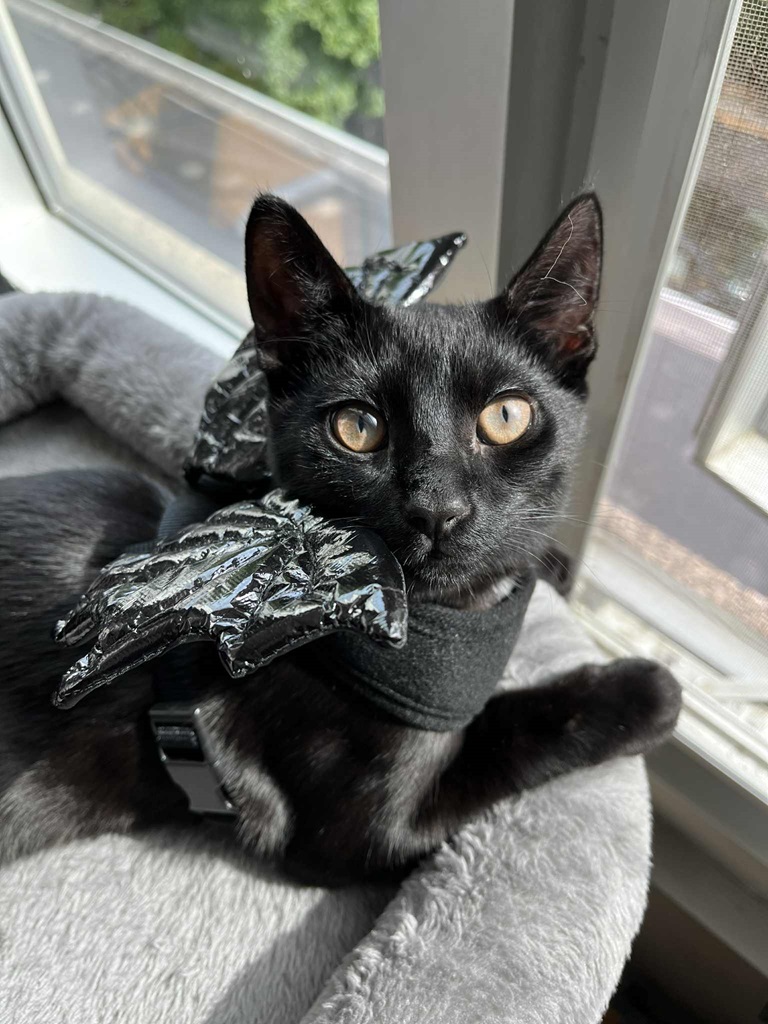
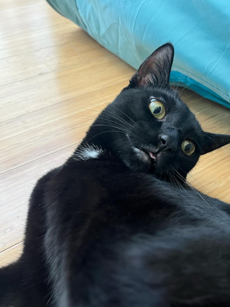
and part of the inspiration for taking this class. I also have a black cat named Raven who has already made an appearance in some way for a few homework assignments (see weeks 1, 3, 7). So of course the obligatory cat
tax is below.
Ethical AI Usage and References
I have only used AI to style my website and to assist with minor formatting changes based on the initial css styling that was generated. This AI usage was done through the Cursor IDE. Otherwise, all content
written for this class has been my own work. Luckily, I have worked with HTML and CSS quite a bit before, so I am hoping to handle the rest of my website creation now that it looks nice and is set up well.
If I encounter problems that are not easily solved with a google search, I will likely ask for more advice/help from the cursor AI. The transcript for styling the site can be found
here.