Week 6 - Electronics Production
This week was all about taking the circuits we learned to make last week and actually making them. We covered details on traditional PCBs that can be sent out for fabrication externally, as well as the tools we can use to make PCBs in the shops here. These mostly involved using the CNC mill, the laser cutter, and the vinyl cutter.
Assignments:- As a group test the design rules for in-house PCB production
- As a group submit a board to a board house
- Make and test a microcontroller system that we designed
- Extra credit: Make a PCB with another process
PCB Milling Design Rules + Board House
On Thursday we had a training session with Quentin on the Carvera where he showed us how the tool works, how to load our files, and generally how to care for the bits. After the training session, we cut the design rule board on the class site and looked at the smallest lines and gaps that can be formed by the tool. Details are on our class site and are found here. Also included on this week's class page is submitting a board to a PCB house. This can be found under the JLCPCB section.
Make a PCB and Microcontroller System
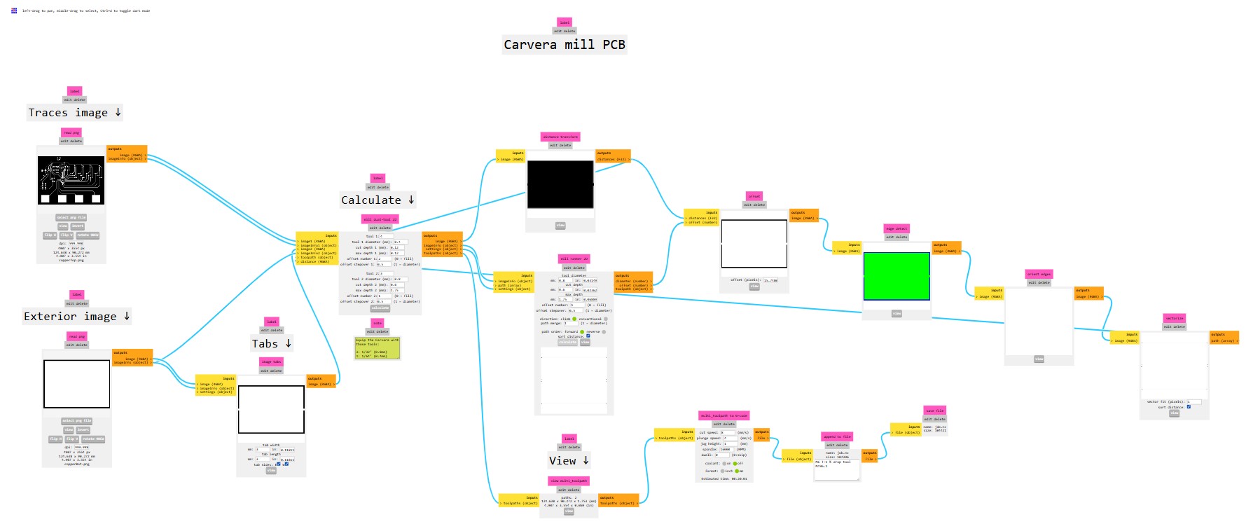
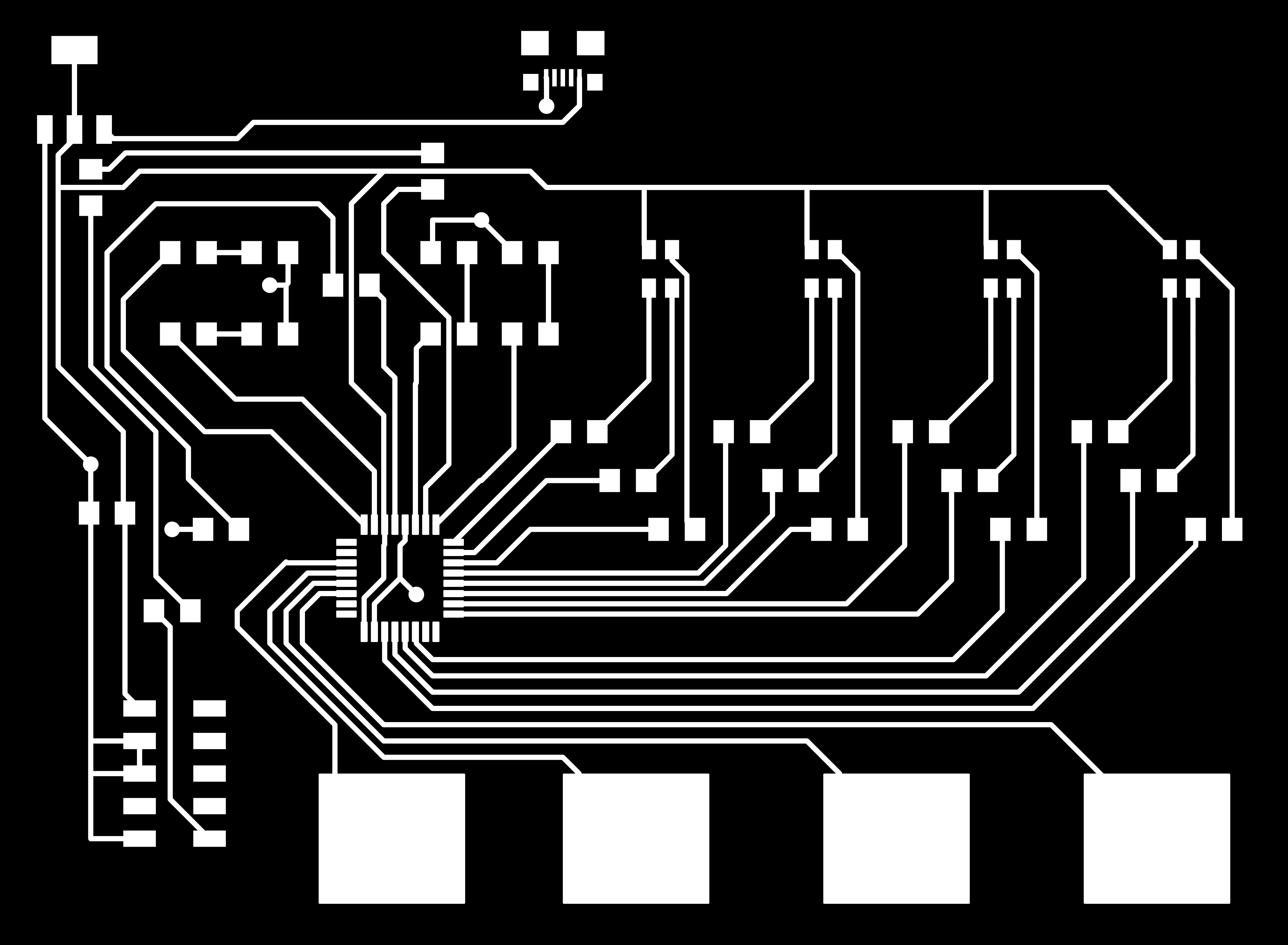
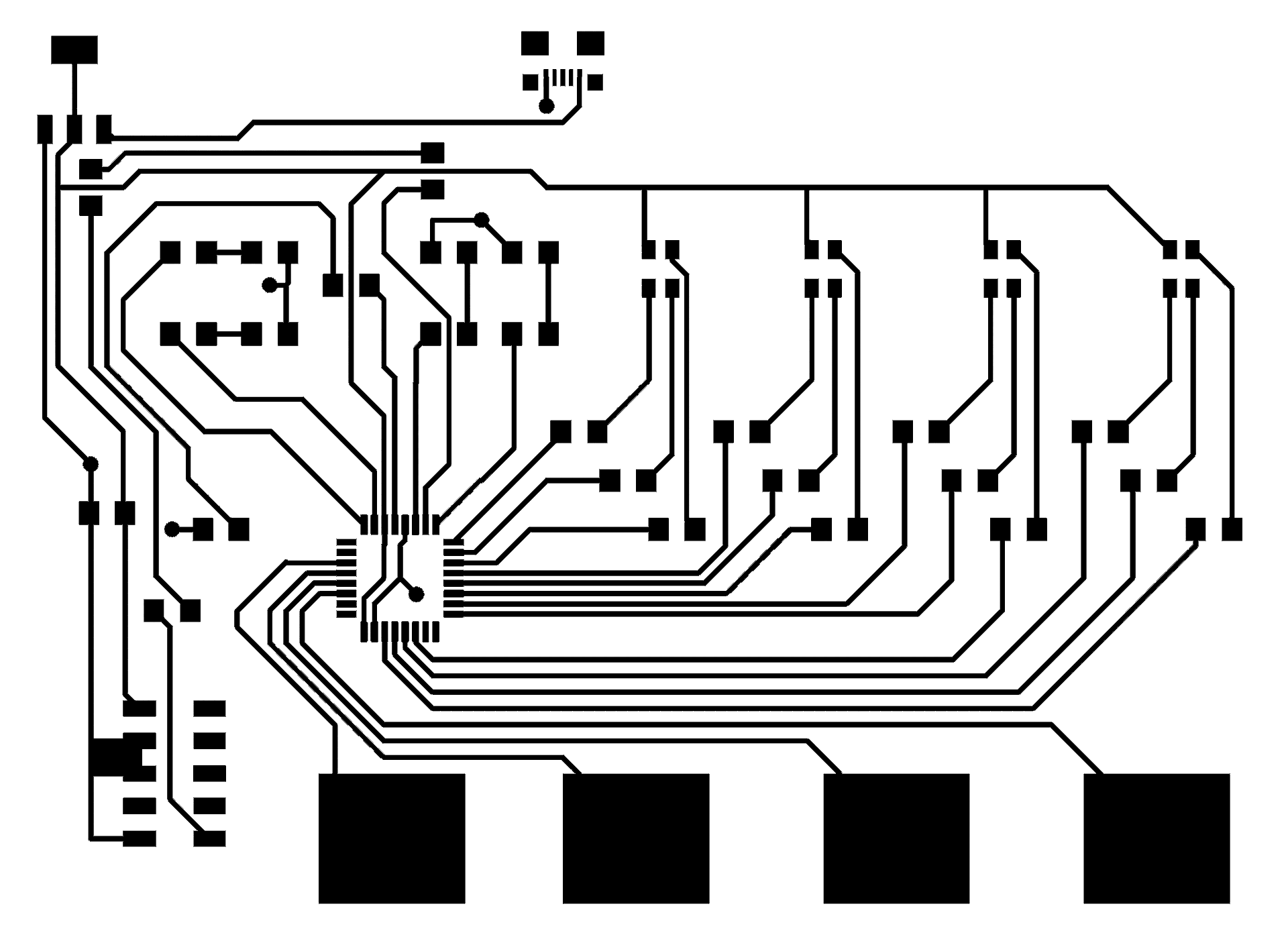
For the PCB design, I chose to make the board that would be able to play the mastermind game that I created and designed last week. I did make one major change to the design however, and that was to make it more compact. I had started to go through the process of generating the g-code (more details below), but I found that my board size was much larger than I thought it was going to be. I spent a decent bit of time shrinking the footprint to make sure that it could fit onto one of the moderately sized pieces of stock, and I finally got it within the target sizing. Other than that, there was no difference in the actual functionality of the circuit, and the updated schematic is linked at the end of this section.Onto the actual board making. Quentin put together another amazing guide and I largely followed his instructions there. I started by exporting my fusion PCB to gerber files, and used another of Quentin's tools (gerber2img) to convert the top copper, bottom copper, and vias to PNGs. I needed to do all of these layers since I planned on using a ground plane as the back of the board. One key thing I learned was to start with the largest footprint gerber file, either the outline of the board or in my case it was the ground plane. This sets the maximum dimensions and the center point, which when locked guarantees that the rest of the layers are within the bounds of the outline. I spent a few minutes trying to debug why my ground plane kept getting partially cut off and this turned out to be the cause.

With my PNGs generated, I then used mods to generate my g-code. It was pretty easy to follow the flow of mods, and Quenten had also given us some pointers during the training session. I started by putting my top copper and ground plane in as the trace and exterior images. I made sure that the tabs were enabled to prevent my board from shifting and potentially breaking anything, and then simply generated the g-code. After processing, the tool path opened up and it looked good. I moved the g-code to the Carvera, mounted my board, set the xy offset, set the z measurement grid, and then started the job.
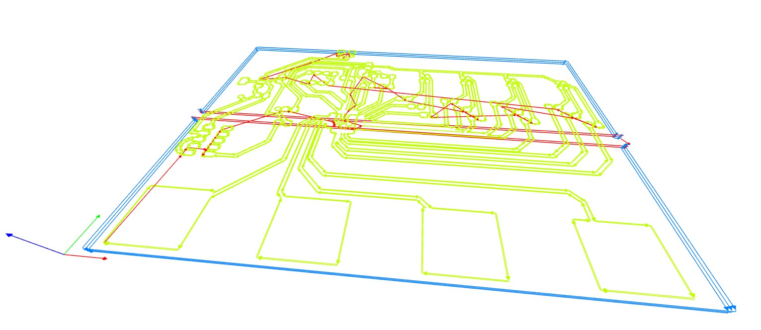
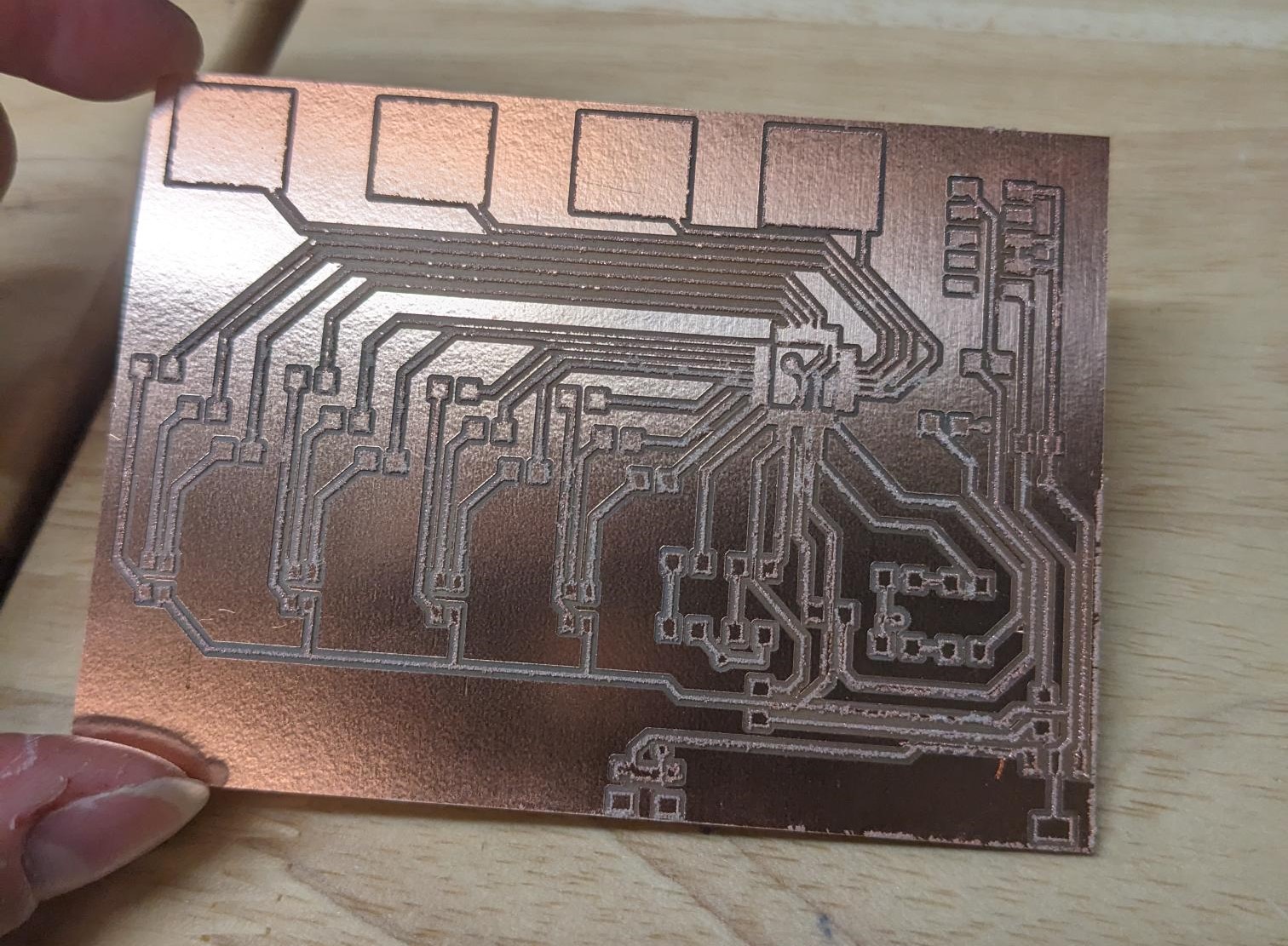
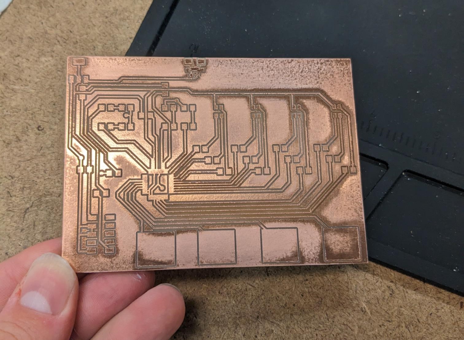
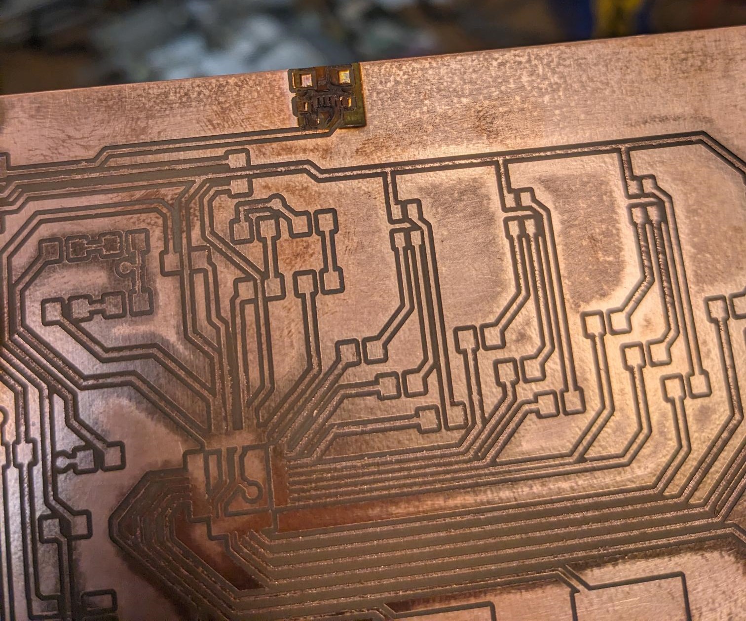
My PCB took about 30 minutes to mill since it was a bit on the larger side, but it came out looking pretty good. The left image below is right after it was milled, and the one on the right is after I sanded down the front a little. A lot of the traces came out really well, and I could definitely have sanded it down further, but the major issue to point out is that the pads for my surface mount SAMD21 and micro-USB connector did not resolve. I was worried that this would happen, but during the training session Quentin said that the 1/64 bit should be able to cut the pads. I am not sure if there were code or settings changes that needed to be implemented on mods, but in a last case scenario I can cut the traces by hand.
I had anticipated making a board using the laser cutter (which we learned in class will produce smaller features), so for the rest of this section the soldering, programming, and testing will be on the laser cut board. Details on how the laser cutting went are in the below section discussing alternative paths for making PCBs. When it came to populating the board, the process was pretty straight forward. I matched all the parts to their locations and soldered them down easily with an iron. For the SAMD21, I used solder paste and the heat gun which also went quite well. I did have to double back and touch up a pad or two with more paste but I ended up with no shorts between neighboring pins which made me really happy. The part that took the longest was getting the gnd vias connected to the back plane. I started by soldering header pins on the front side to hold them in place, before trying to solder the back to the ground plane. I knew it would take longer because the large sheet of copper distributes the heat very well, but after an attempt or two with the iron I moved to the heat gun. I then touched up the solder on the front side of the header pins and clipped them off. Unfortunately, I also realized that I forgot to include the CLK and IO on the 2x5 pin header so I added two jumper wires to the correct pads of the SAMD21.
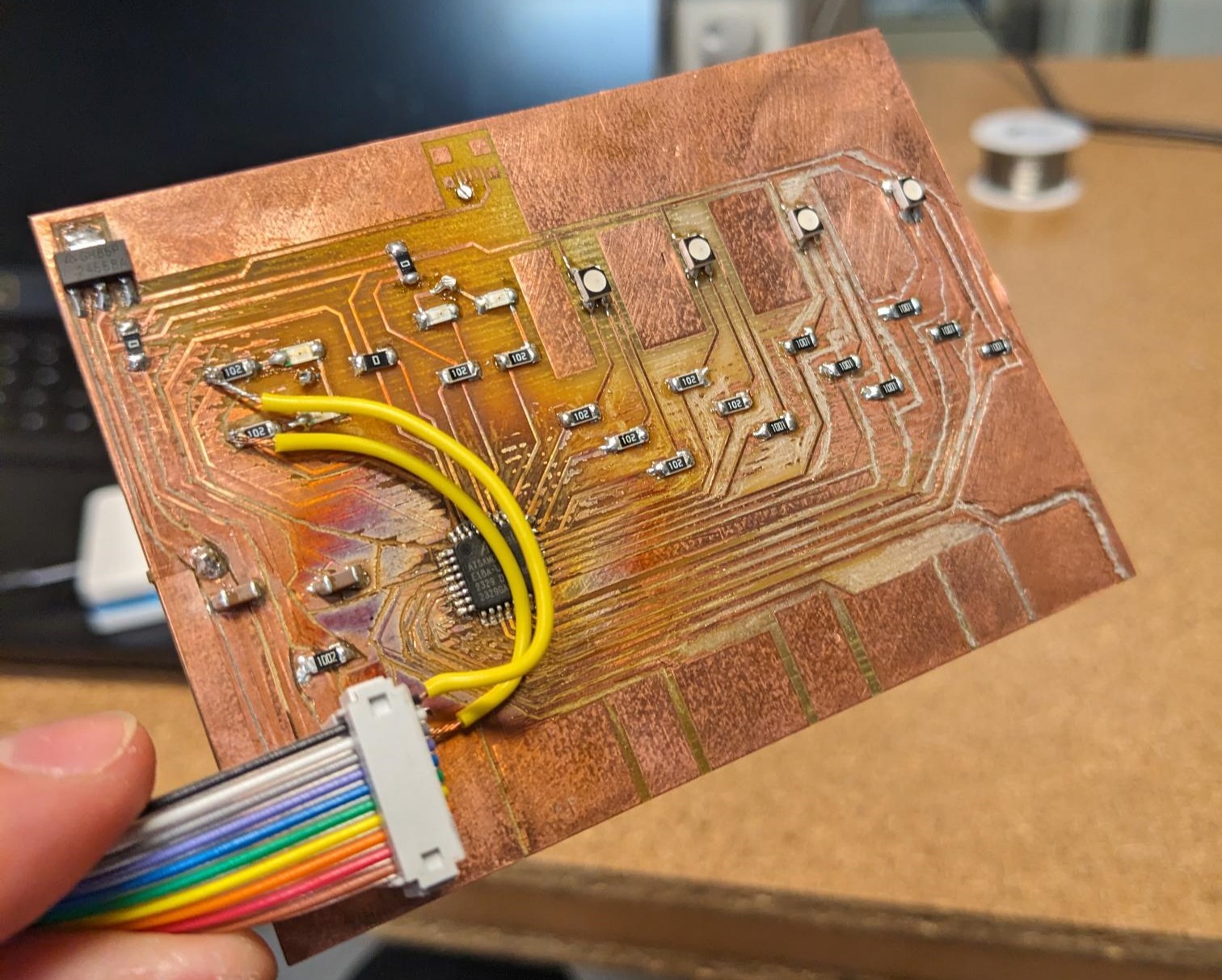
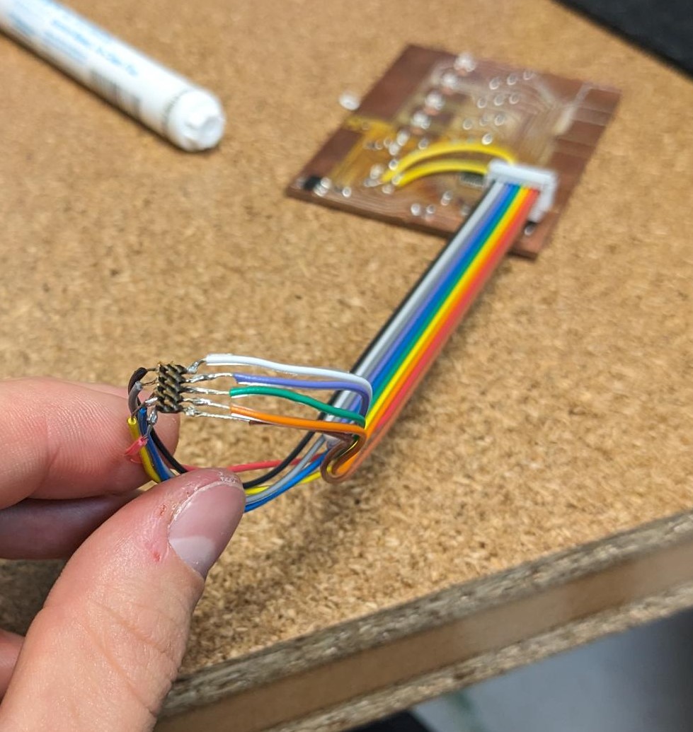
With the board completed, I then ran into more roadblocks this week with trying to get it programmed. The CBA electronics lab did not have the right cable/programmer combination to connect to my 2x5 connector. I had tried to use the same one from the electronics lab session with the intention that it would be plug and play, but as was my theme this week that was not the case. One programmer had the right sized 2x5 connector, but there was no cable that would connect it to a computer. The other programmer had the right computer connection, but not the right 2x5 pin header. I ended up crudely assembling my own jumper that would transition the smaller form factor 2x5 on the programmer to the larger 2x5 connector on my board. As janky as it looks, nothing is shorted and all lines were intact.
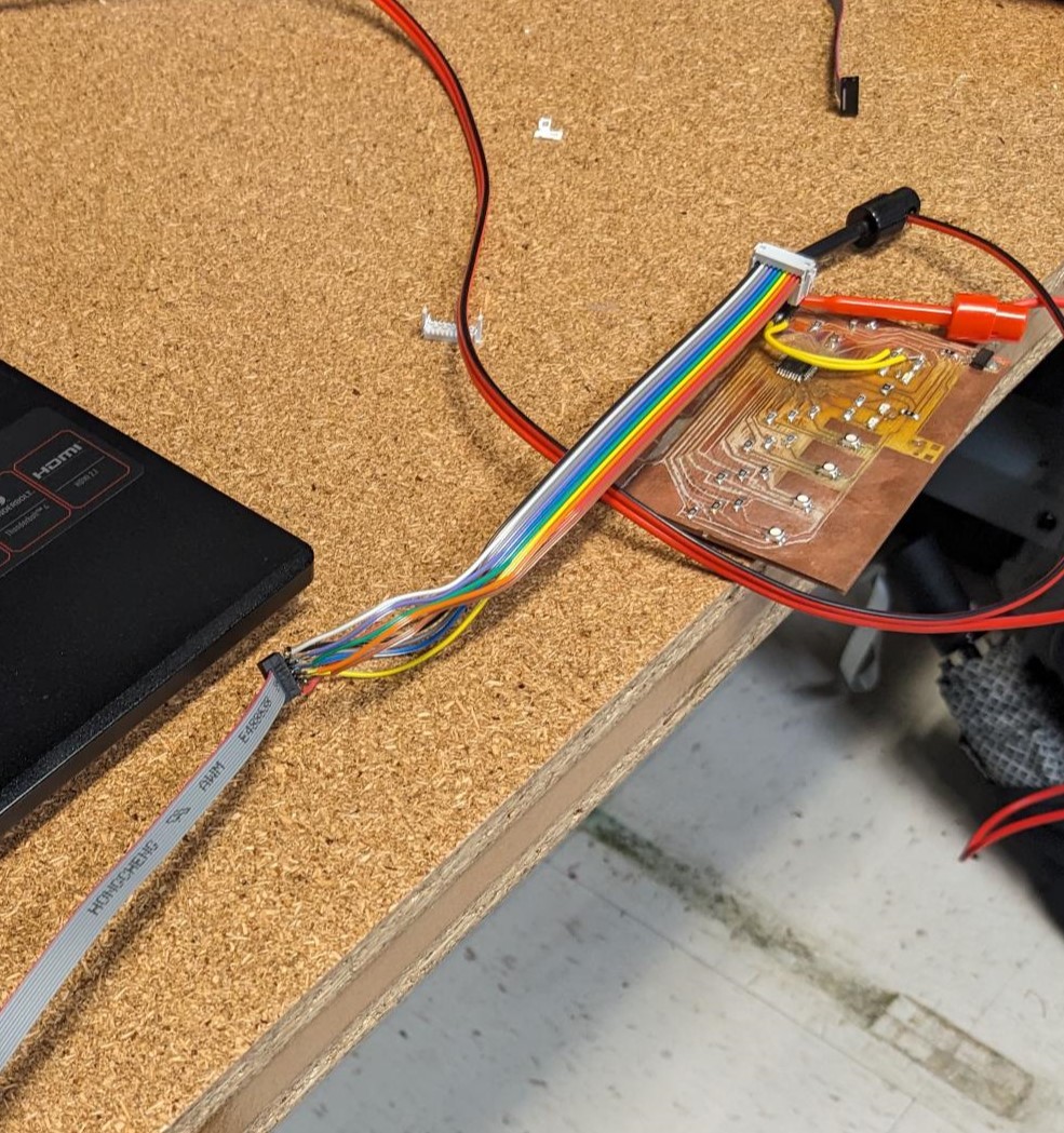
Since I still did not have a micro-USB, I did not have power going to my board. So I used a power supply to deliver my 3.3V and on startup I did see my SAMD21 draw about 5mA. However, the last problem that I was unable to tackle was that I could not get the programmer to work. I tried following the guide linked from Week 3 on programming a bootloader, but every time I tried to run it I got the error below. I tried by selecting different programmer types, I tried matching the settings in the guide exactly (even though I was using a D21 not a D11), and I tried reversing my cable just in case I got the polarities wrong. Everything I tried though had the programmer fail at the same step.
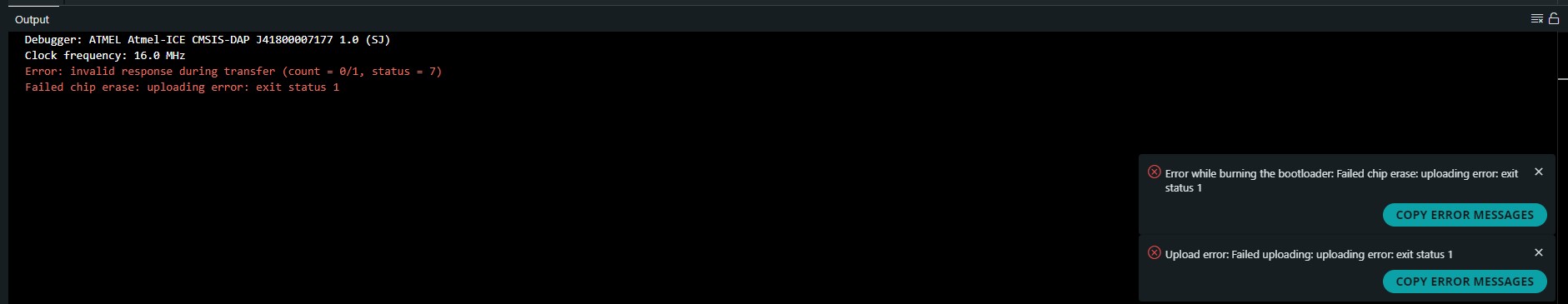
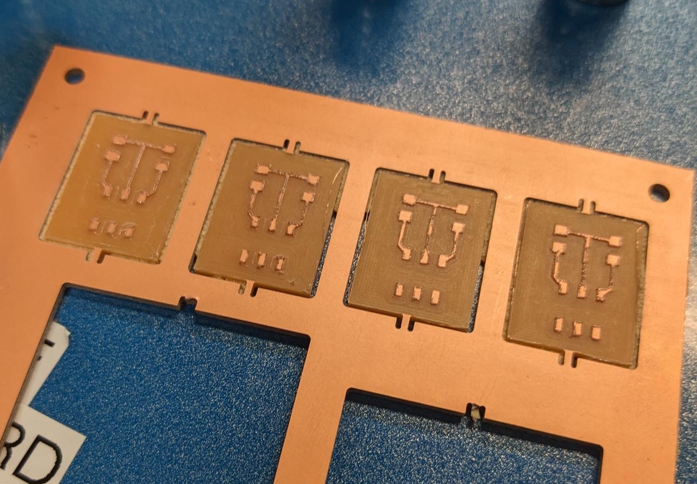
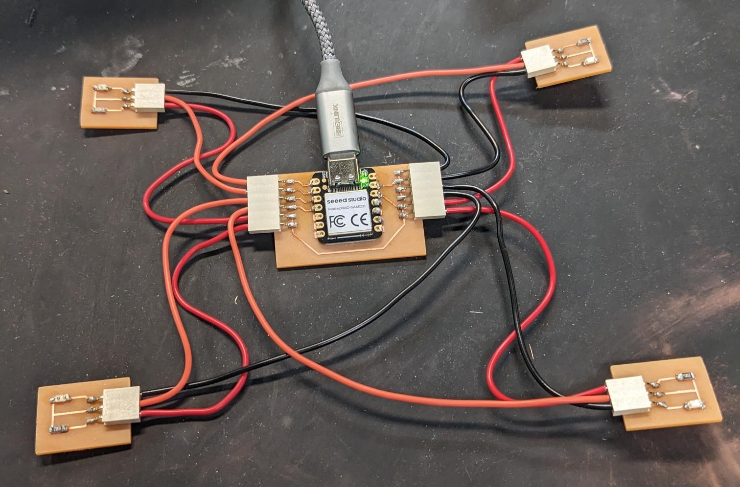
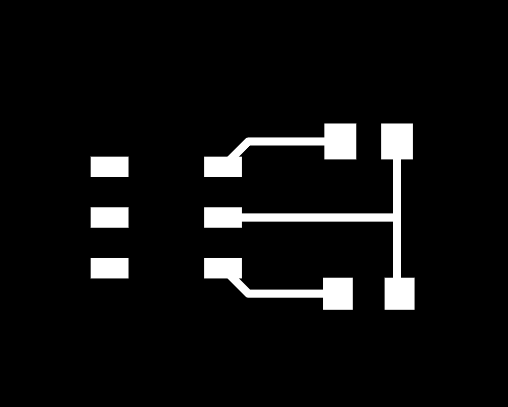
I am honestly a little disappointed I was unable to make it work, but after a bunch of additional debugging when I had the time over the following weeks I believe the issue is related to my computer being able to recognize the programmer. I found a couple of threads on various forums talking about potential fixes, none of which I was able to get working for myself which is unfortunate. The other downside to having this issue is that all of the future boards I decided to make made use of XIAO microcontrollers and I think it would have been very fun to continue to use surface mount ones. In either case, below is a separate board I made during Week 8, input devices. More details on the actual fabricaiton of it can be found on the Week 8 page, but I followed the same process for the carvera as I no longer needed the laser cutter to cut the right trace sizes. It makes use of a microcontroller to read the voltage level of a couple of phototransistors which I also made PCBs for. This board did work successfully, and the code is also included on this page.
Making a PCB Through "Laser Cutting"
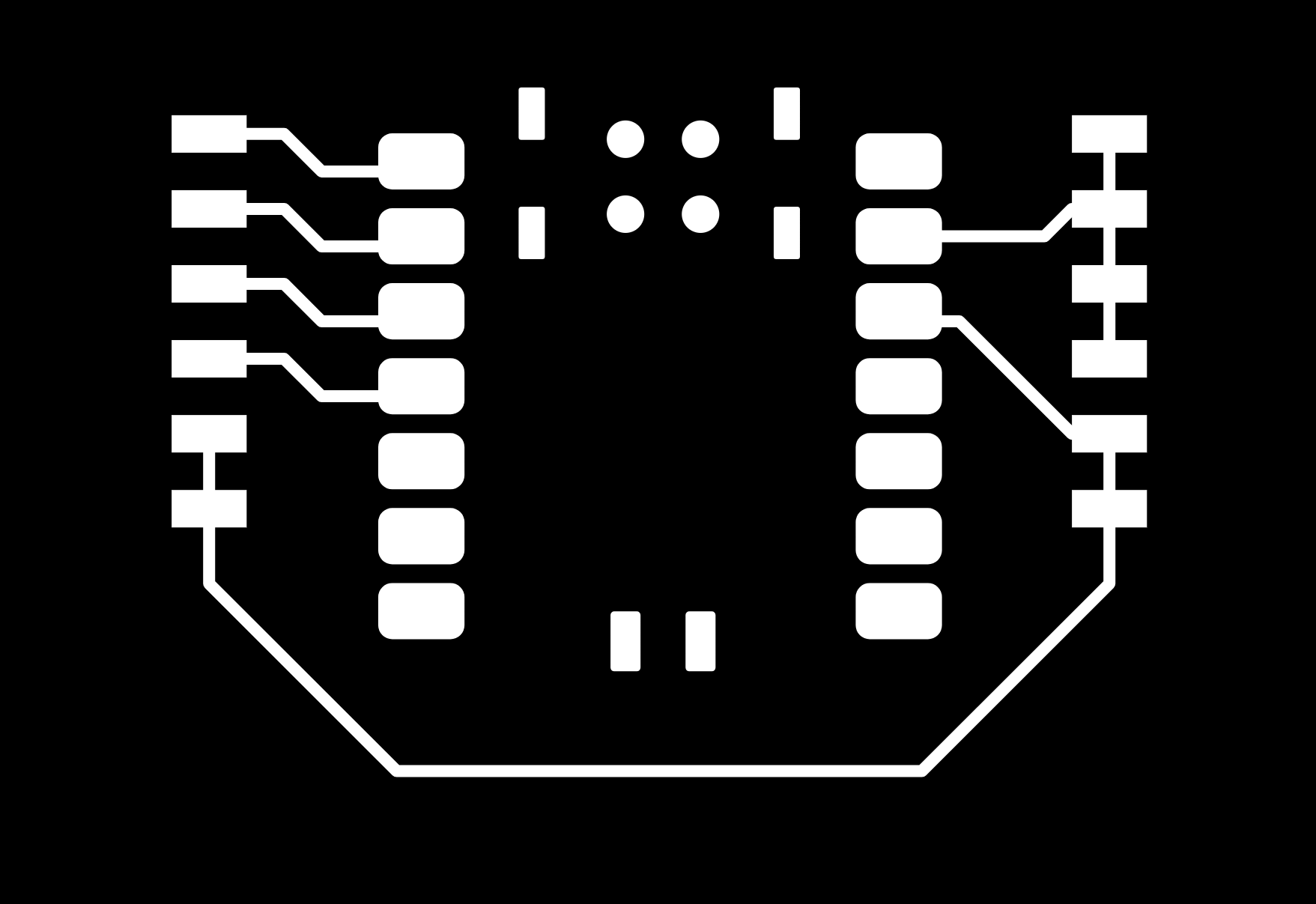
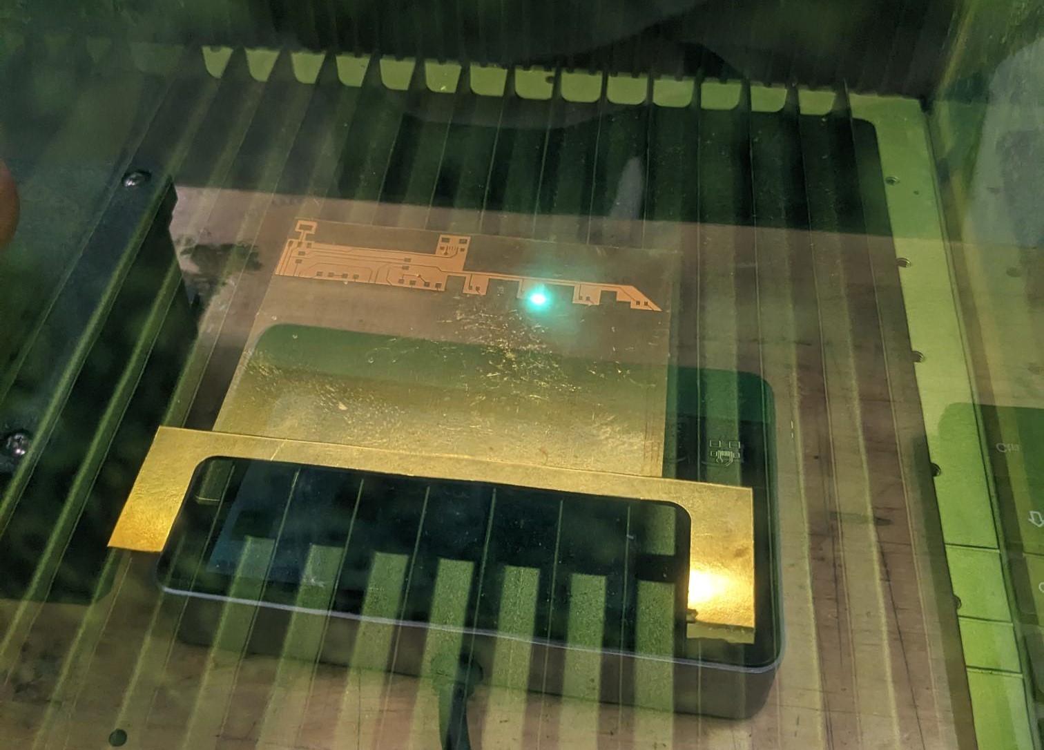
As much as I would have liked to put my stock into the laser cutter, upload my file, press go, and get a great looking PCB out of it, that's not exactly what happened. Luckily the wording on the class page is to make a board through "another process" so my zombified half-laser cut half-manual weeding I guess counts!Alright, so as mentioned in the above section I had planned on laser cutting a board since I needed to get the precision required for a surface mount SAMD21 and micro-USB connector. This process still started at the Carvera, because I at least wanted to cut out my board footprint and try to cut the vias. The first board I made did not include the vias, and I figured worst case I could use a drill press to cut them after. But for this board, I combined my vias and ground plane into one image and ran it through mods. I then cut that board on the Carvera and got my board footprint with my vias cut into it (I should have taken a picture of it but I forgot). I took my board and some scrap stock up to laser cutter and here is where my challenges begin.
I started by following this guide that was linked from the class website. Overall it was very well written, except for the fact that I had created my designs in Fusion not KiCAD. This turned out to be a major problem because there is a specific export feature of KiCAD that produces a dxf for the laser cutter with the traces outlined. That way when cutting (or engraving in this case) the PCB the traces are left untouched while only a small area around the traces is removed. (*Note that I did create a file that would engrave my entire PCB area, but it would take 3 hours to run so I did not use thah file). I spent too much time trying to figure out if there was a way to export a similar file from Fusion before finally downloading KiCAD. I then spent was too much time importing my gerber files into KiCAD only to find that the export dxf function just produced the exact same dxf that Fusion does. This led to spending too much time again trying to debug KiCAD by testing it on a quick circuit designed entirely in KiCAD (suggested by Alfonso, did not work sadly) and by updating all the design rules to see if it was basing the outlines on those. Nothing would produce the trace-outlined dxf even close to what the guide showed, so I started testing if I could cut or score the traces into the stock instead of engraving them.
I ran a number of different tests on the scoring and cutting modes on a scrap piece of stock. Unfortunately, I found that once I got through the copper so they were not creating shorts, all of the small features like the micro-USB pads just flew off. This was not the case with engraving which is why that method is the preferred method for creating PCBs. I did also verify the power and speed parameters provided by the guide by cutting just the micro-USB area, so that was at least useful to test.
I then had an idea to manually outline my traces in a png file, so I once again spent too much time crudely removing a large portion of the empty space of my PCB in the hopes that it would reduce the job time. But once again this proved futile because the png that I imported into the software did give me access to the full set of settings since it wanted to engrave an image not a vector/object file. I then had an idea to try and cut out just the micro-USB from the milled PCB since it only takes about 2 minutes to run. I put my PCB in, aligned the z, cropped to just the micro-USB, and started the job. Sadly this did not work either. Even though the image was placed right where it should be, there must be some slight misalignment and the cut came out offset.
Ultimately, what actually ended up working was modifying the initial dxf that I exported from Fusion. I loaded it into the laser software, and spent ~5 minutes drawing rectangles over empty space and then using one of the intersection features to cut the rectangles out of the design. This brought the engrave time down to 45 minutes and at that point that was good enough for me. About 15 minutes in, I saw the board bowing pretty significantly. I paused the job to see if the heat was causing this, but the bow never recovered. So I just continued the job and I would just have to make the result work.
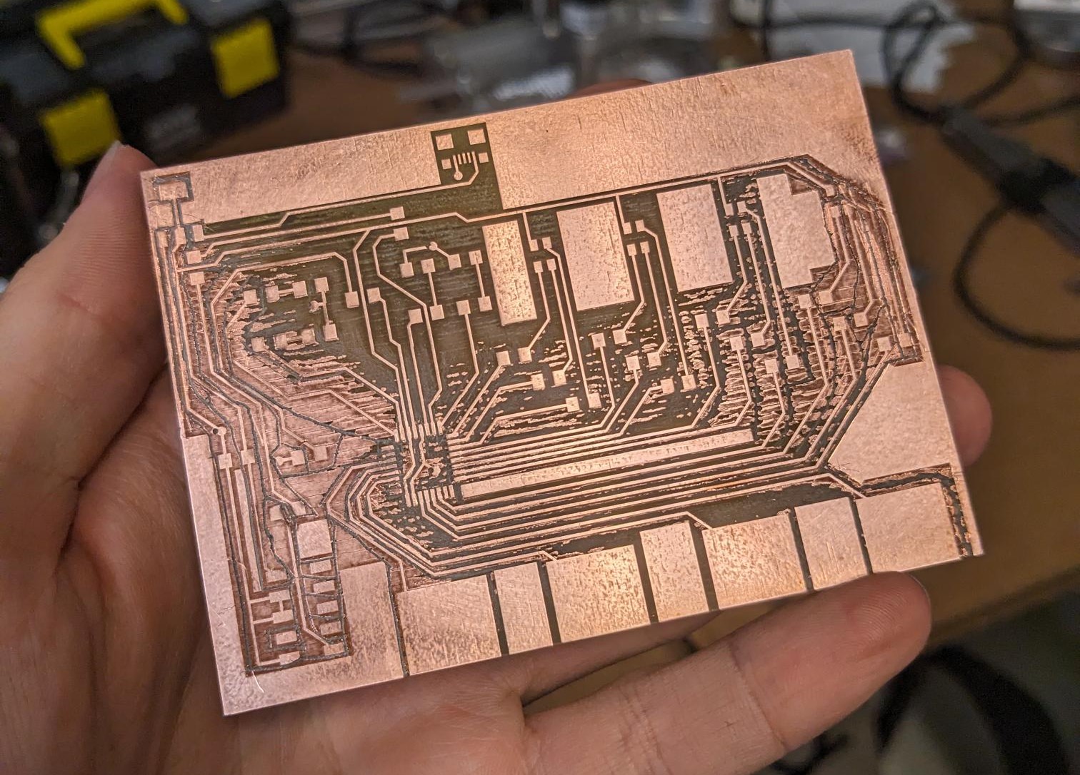
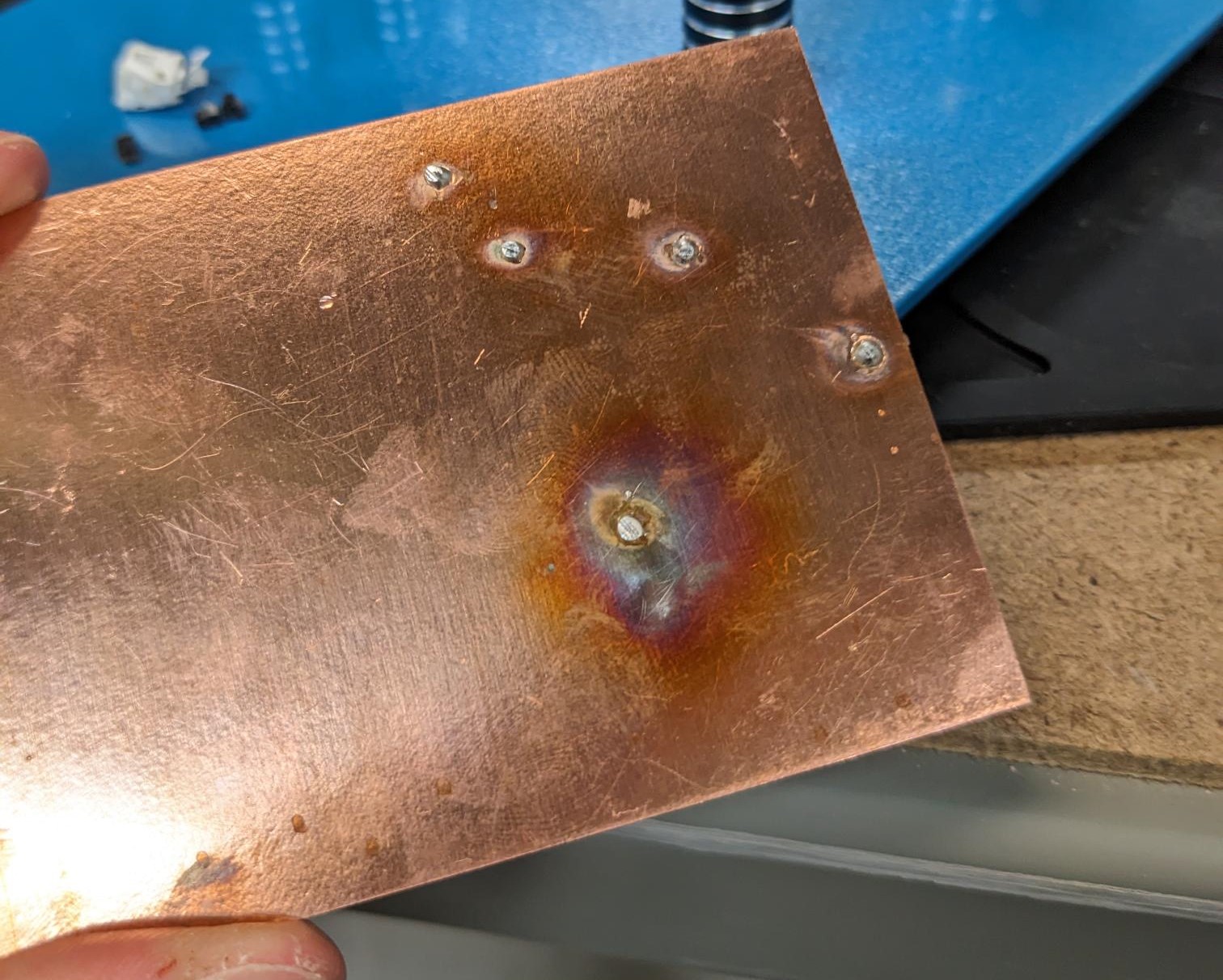
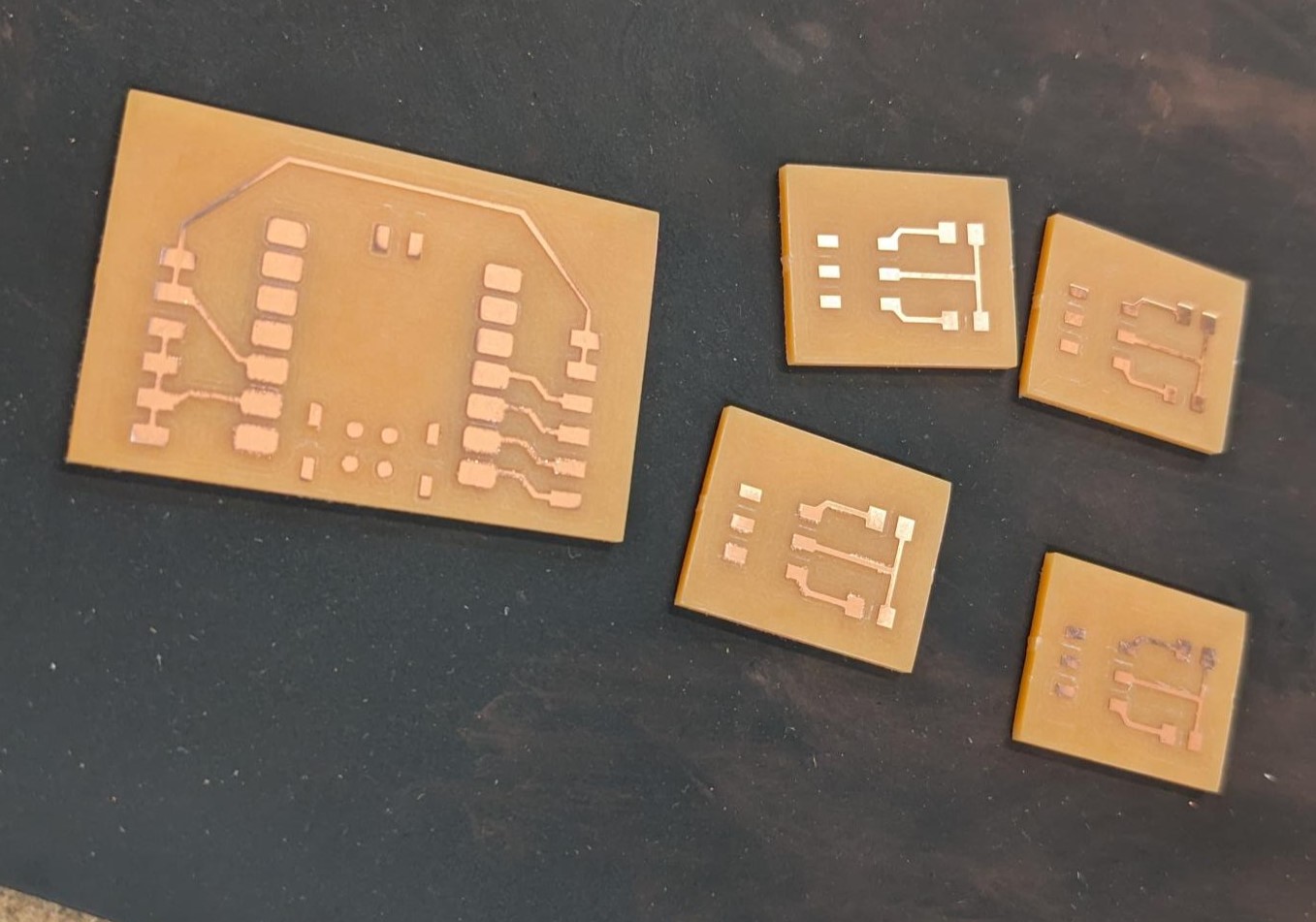
Even with the bowing, a large portion of the board cut pretty well. Even though it may not seem like it in the image, a portion of the copper between the traces was a thin leaf-like layer that scraped away pretty quickly under a bit of applied pressure with tweezers. And for all the time I had put into the board this far, spending 10-20 minutes cleaning up the traces was not too big of time sink. That being said, the traces on the edges of the board did require a lot more force to get through, they ended up requiring some moderately deep scoring as opposed to light scraping. However, I still prevailed and when testing all the traces and pads with a multimeter I did not find any shorts!
I must say though, despite all the challenges I had with the laser cutter and how painstaking it was to try and get the right file to actually cut into the stock, I do still prefer this method. The traces come out much cleaner and the resolution is quite important when it comes to surface mounting some of the smaller packages. Starting with a larger board definitely did not do me any favors, partially due to the cut time and partially because the larger board will bow much more (if it wasn't heat I would guess it's due to the mechanical stress imparted by the lost copper layer?). And I guess I also got a lot of practice making traces by hand so that's useful to have as a backup right?