Final Project - Lithography Exposure Tool
About My Final Project
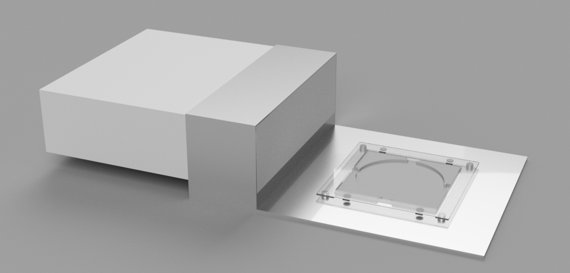
For my final project, I have decided to make a crude photolithography exposure tool. Photolithography is the most important and critically controlled step in semiconductor manufacturing as it is the process that determines the actual size of the features that get created. I have used many direct write (serially draws a pattern like 3D printing) and stepper (projects an already existing pattern) exposure tools. They each have their own benefits and drawbacks, but when it comes to passion projects these tools are extremely cost prohibitive and require a lot of support steps. I have some projects in mind that I would love to do with the use of photolithography, and I wouldn't even need a top-of-the-line high-resolution tightly-controlled machine. I could very likely get by with a very simple near-contact exposure tool and crude printed masks on transparent film. As such, I have decided to make the photolithography exposure tool I would need to be able to do my own basic photolithography processing!
Updates From the Midterm Review
My midterm review went very well! I had been making quite a bit of progress on the side of the weekly assignments because I already had most of my parts made. At this point, I had the metal plates cut to size but not milled, all of my acrylic was laser cut, and I had soldered my light board but just needed to add new voltage regulators. Alan did not have any concerns with my project getting completed on time which was a good sign.We also talked about what needs to be done to complete the final project and what the expectations were for getting those tasks done. I needed to size all of my screws/fasteners, but I had actually planned to do that right after my review completed (and I did). I had scheduled time with Dan to take a look at milling my metal parts on 11/21, during which I was also going to print an additional fixture I needed to hold my wafer alignment pieces in place. On the electrical side, I will need to make a control board that will have a XIAO, USB-C power regulator, and a touch screen if all goes well. I will likely print a housing for the touch screen and affix it to one of the front corners of my base plate. The control board will also require code that will set up the user interface and activate the light source for the user-specified amount of time. Luckily, I plan on getting exposure to the touchscreen in the networking assignment and I will work on the user interface for the interface/application assignment. All in all, the remaining work for my project consists of a few machining tasks, a couple of prints to run, a PCB board to design and make, and a program to write. Some of which will be completed as weekly assignments which definitely helps out on the time management side of things.
Sections:- Initial Planning and Sketching
- Creating a Proof of Concept Model
- Refining the Design and Creating a Realistic Assembly
- Printed Parts
- Laser Cutting Acrylic Parts
- Water Jet Cutting Aluminum Parts
- CNC Milling Aluminum Parts
- Hand Finishing Aluminum Parts
- Electronics Design
- User Interface and Control Code
- Final Assembly
- Testing!
- Outlook and Future Work
Initial Planning and Sketching
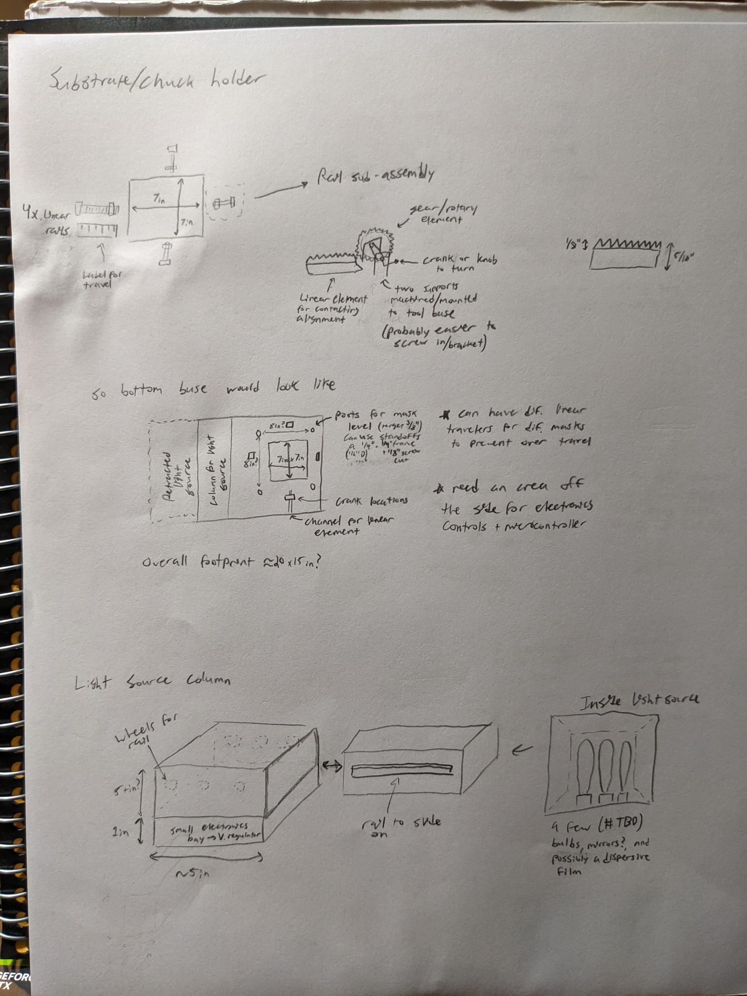
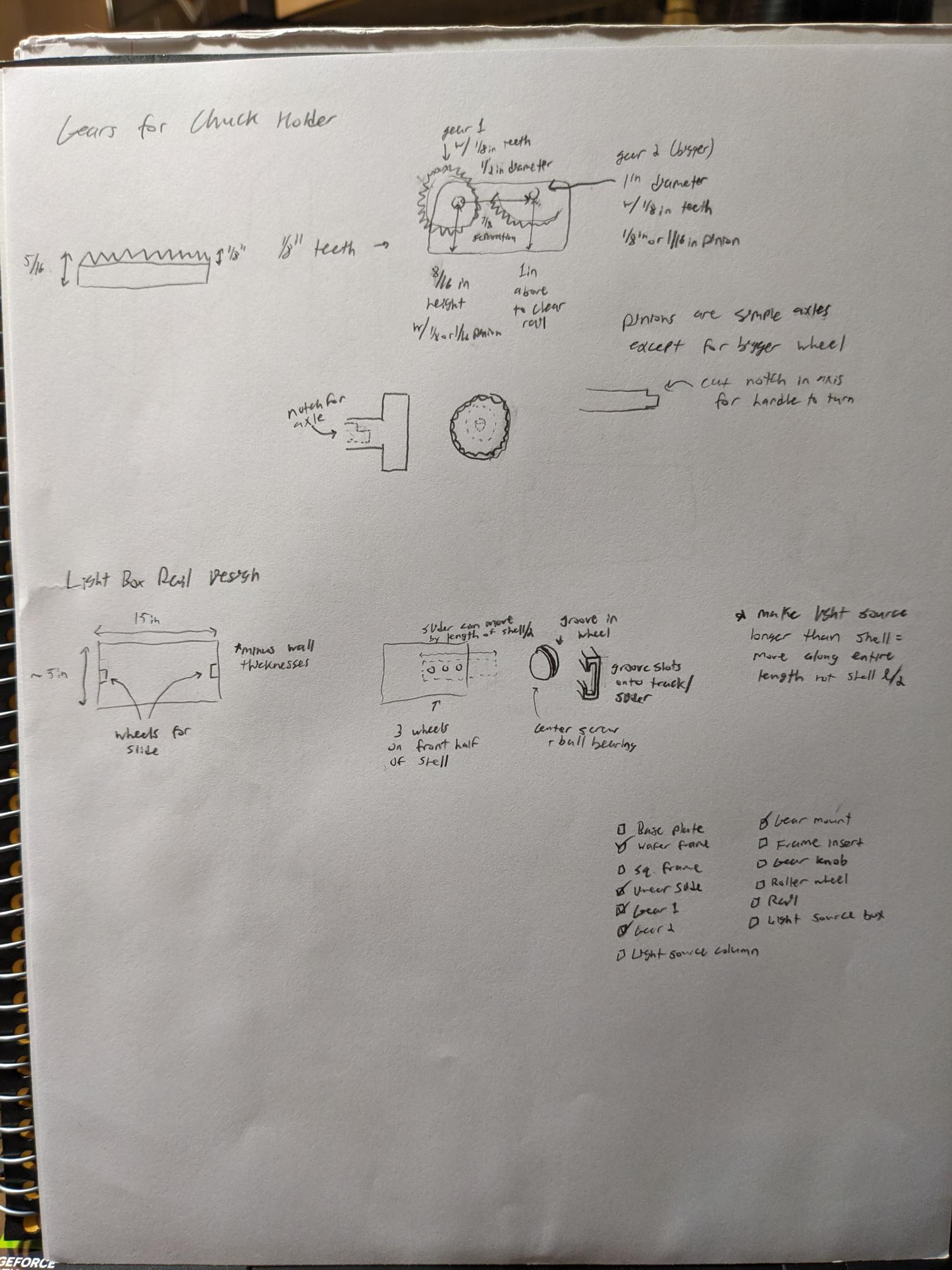
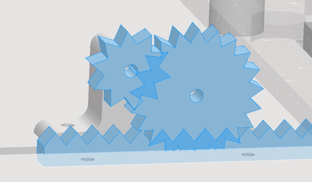
The below images are of the initial sketches that I created when starting to think about the different components that would be needed for this idea. I initially wrote out some of the main characteristics for this project, namely the compatibility with printed masks and the ability to take multiple different substrates. Following the initial sketch, I came up with some ideas for sub-components that are needed like the chuck frame and the light source column. As I was drawing these sections, I was able to further break out how I wanted to design individual components to accomplish the goal of the sub-assembly. A prime example of this would be the gears and linear toothed rail/slide thing. Initially, I planned on using a set screw for the alignment. But after trying to figure out how to translate the rotational motion into a different direction I realized that I could keep the rotation in the same plane. The result is the sketch of what I called the linear element (because I have no idea if there is an actual technical term for it) that consists of a gear that will turn and move the slide based on the interlocking teeth. The last things to point out are some initial ideas for how to slide the light box out of its housing after the substrate has been aligned, and a checklist I came up with for parts that I need to CAD.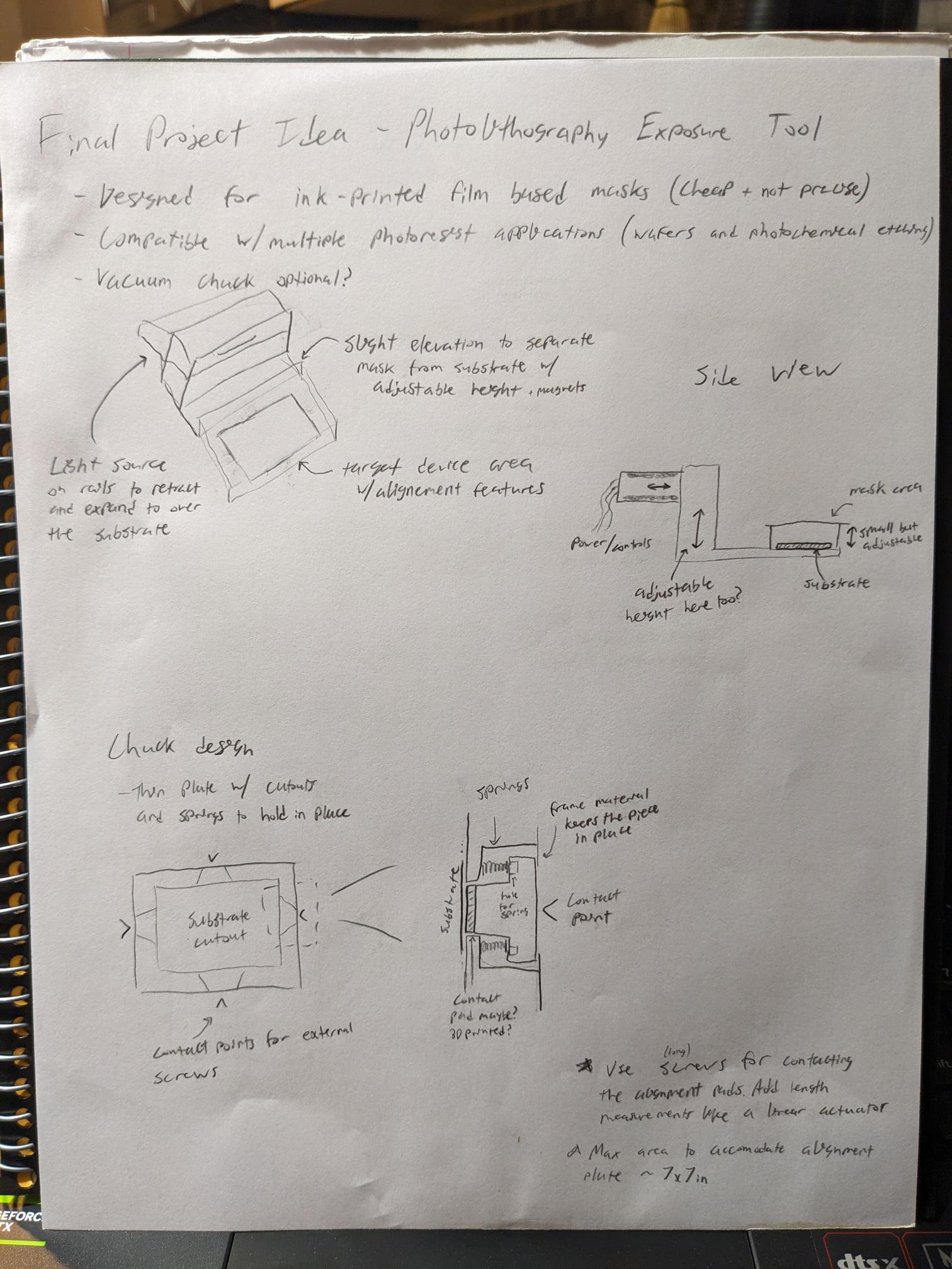
Creating a Proof of Concept Model
Once I had some initial sketches of what I wanted to do, I created a very rudimentary CAD model with approximate dimensions. Not all the components are included, for example there is no gear system in this model, but this helped me get an idea of the dimensions and spacing I would be working with when I actually start improving these designs. As part of the Week 1 assignment, I also used this model to texture parts, render a high quality image, and create an animation.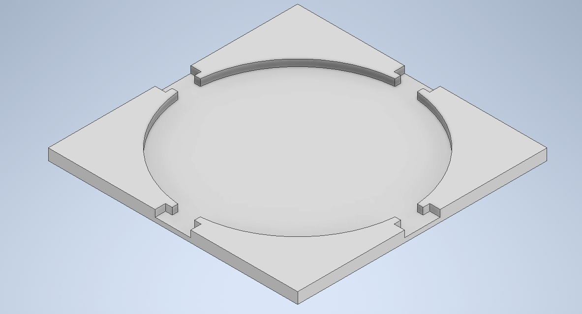
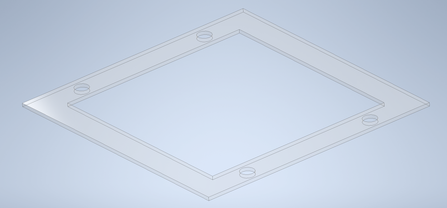
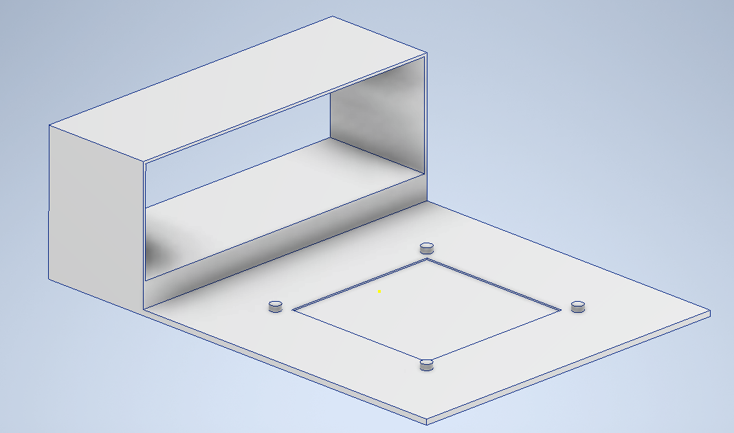
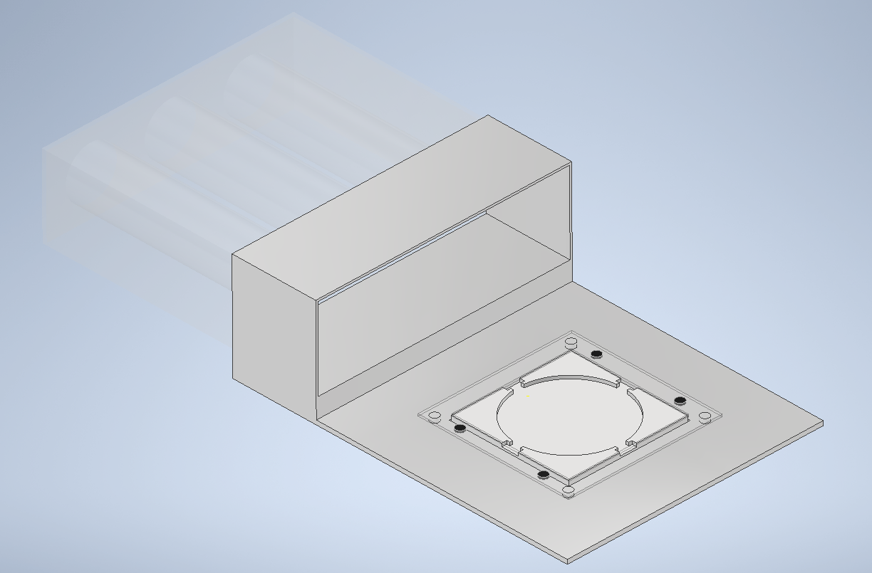
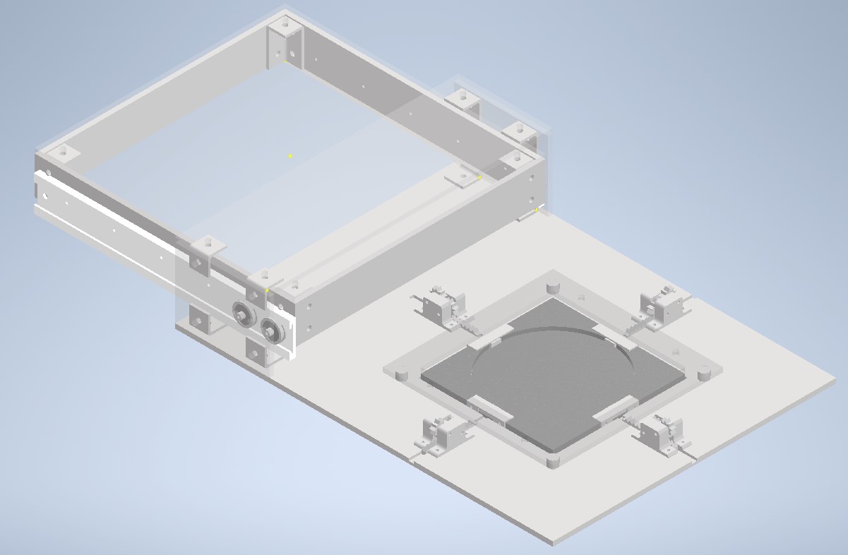
In the above images, the top left picture is of an alignment chuck for a 6in wafer. The central pocket is slightly larger to allow the alignment pads some room to come in from the cutouts on the sides to actually hold the substrate in place. The top right image is a crude drawing of the light box, initially I was thinking about putting bulbs in but now I am going to make my own board with surface mount white or UV LEDs pending some experimentation. The bottom left is the raised frame that will have magnets inserted into the holes to hold the printed mask in place above the substrate, this piece is transparent because I am planning on making it out of a plastic/acrylic material and was playing with material features. And finally, the bottom right is the main body/plate that everything will be attached to. Ultimately the light column will be made separately and attached mechanically, but for simplicity I modeled it all together. This component is also currently made from aluminum in the CAD, but I am thinking that I will likely make it out of acrylic if possible due to material costs. When combined, these components create the assembly seen below. I then imported the assembly into Fusion 360 to handle the rendering and animation.
Refining the Design and Creating a Realistic Assembly
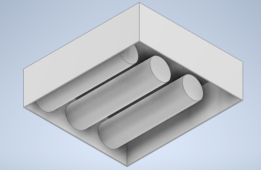
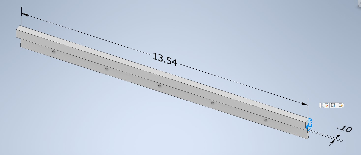
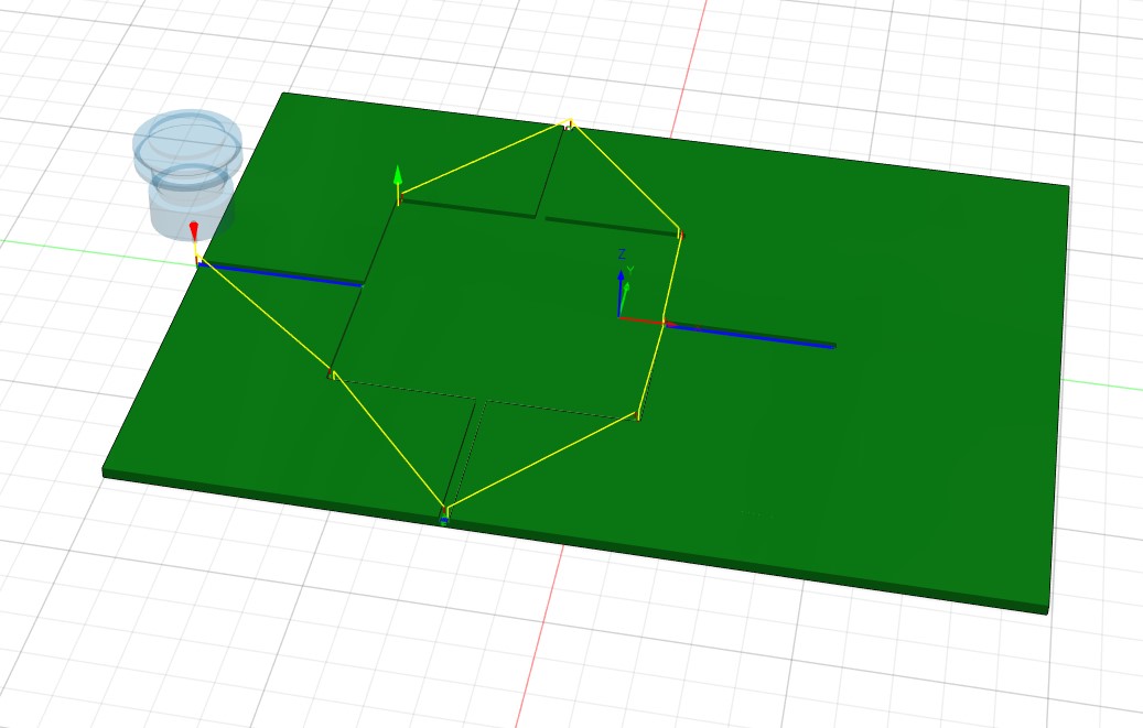
A lot of the CAD work to turn the initial assembly into an actual assembly revolved around separating the main body/plate into its individual components. This needed to be split into the bottom plate, 4 sidewalls and a top to enclose the light source, 2 sidewalls and top for holding the light source, and the linear rail system to allow the light source to slide in and out. The plate, walls, and top pieces were fairly simple to create, they were just rectangular plates with holes positioned at particular locations for assembling them together. I had CAD-ed up some brackets that I plan on 3D printing, so I just needed to make sure that the holes lined up properly. The rail system was a bit more complicated to design though. I had purchased a cheap set of ball bearings off Amazon and I designed inserts for them so they could be attached to the sidewalls of the light column with screws/bolts. I also created a part that would snap onto the outside of the ball bearings with a groove cut into it such that the rail I was designing would seat properly. These parts took a bit of back and forth to make sure I was getting the dimensions correct and that there would be sufficient travel to expose the entire substrate. I could probably have used a double rail to get more travel with less space used, but I didn't know how I would go about designing that at this point in time.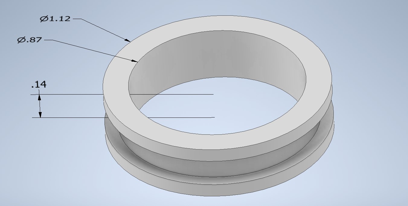
Another area that required a couple of design iterations was the gear system I had implemented to align the substrate. I had CAD-ed all the parts for the assembly in Week 1, and screenshots of these parts are in the Week 1 page. There is the linear toothed component, a large and small gear, and then a mount for the gears. I did not update these designs while I finished making the rest of the parts, but when I assembled them all together somewhere along the way my math was off. The large gear physically collided with the other parts which obviously is a problem, a visual inspection also revealed that the teeth of the gears/rail could potentially jump or catch because the spacing was off, and the light source would crash into gears because the clearance was too low. After a few design iterations, I ended up removing the large gear entirely in favor of two of the same small gear. This allowed me to also reduce the height of the mount, so that I only needed to raise the height of the light source by a tiny bit. This distance was pretty important to me because without expensive controls and optical components the light will spread out more from the point of origin as the light source gets further away from the mask. For the best results and clearest image transfer, it is important to make sure that the light source is as directional as possible, meaning the light has as little time to spread out as possible and therefore should be close to the mask. In the images below the old design is on the left and the new design is on the right.
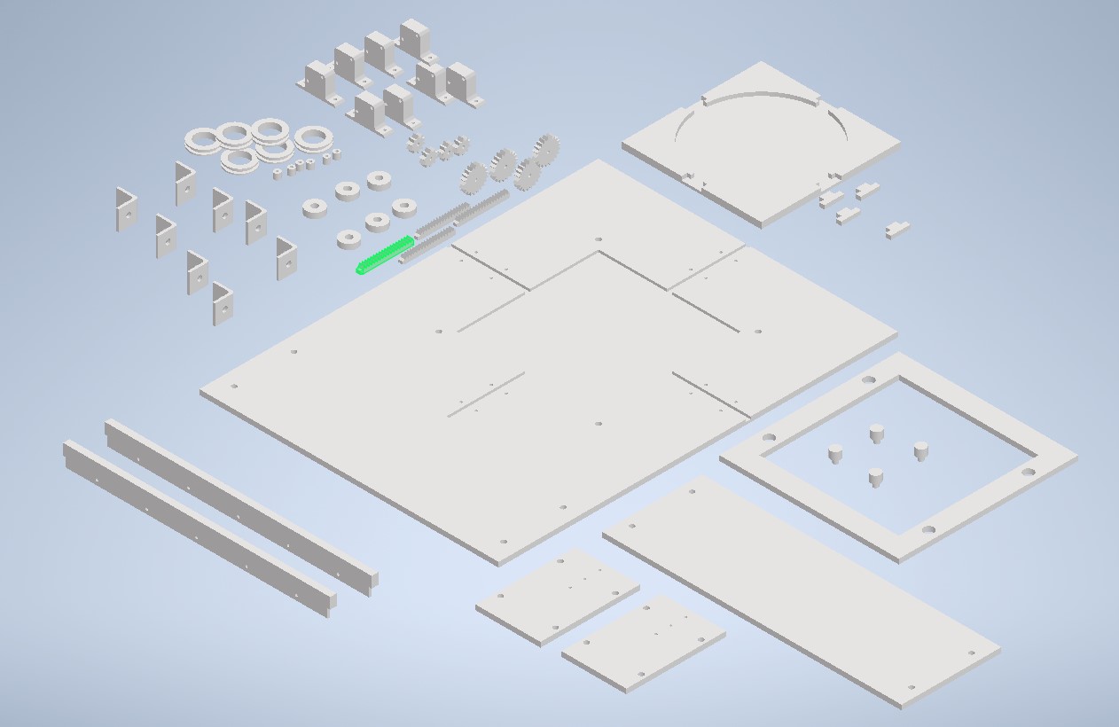
When I started the assembly, I had anticipated using 6 ball bearings and I had not yet updated the gear system. That is why in the picture containing all the loose parts some may not have actually made it into the final assembly picture to follow (also not all the light source parts were included at that point either).
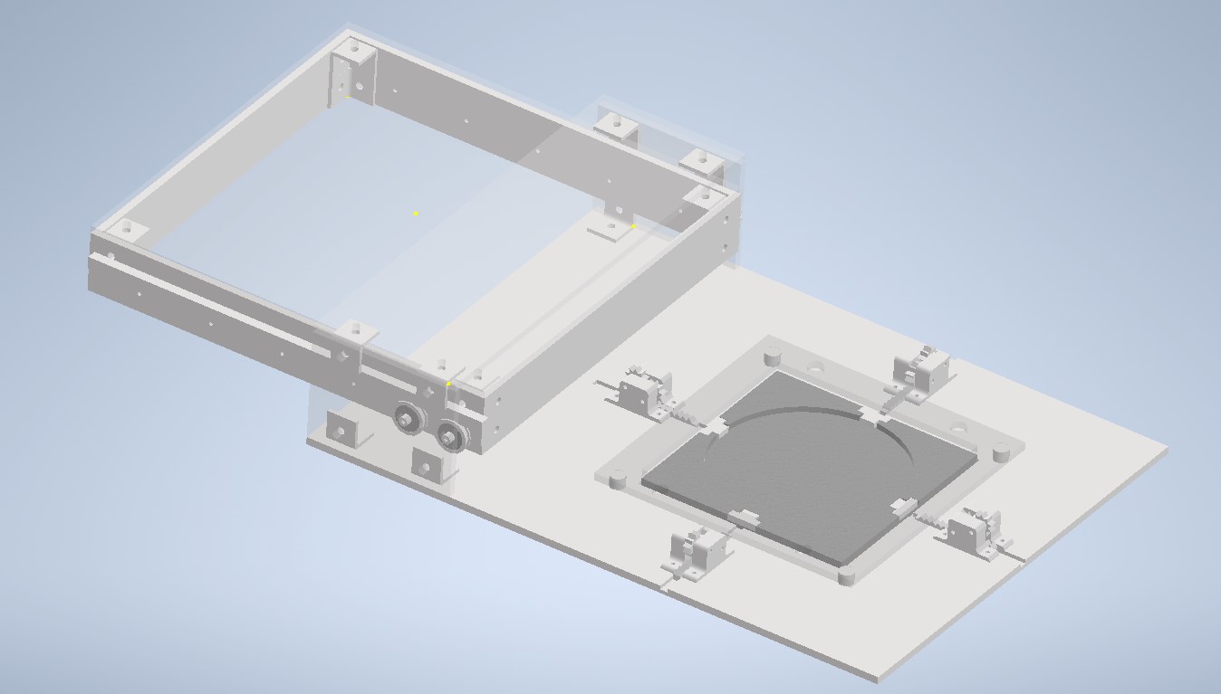
Even with this final assembly however, there are a few additional details worth pointing out that will be addressed after I have a consultation with my TA to make sure things are on the right track. The first of which is that there is no handle to turn the gear system at the moment. I do plan on putting in a knob that the user can turn, but I am not sure if the best way to do this is with a keyed rod that would insert into the gear or to just glue it. The second issue is that there is no counterbalance on the sliding rail to prevent the light box from disconnecting from the ball bearings. I could add a bottom protrusion on the rail to make sure it can't come off, but then getting the rail on the bearing in the first place will be a challenge. There are methods I know I could implement that I know would work, but I would rather get some input from the TA first to make sure I do it in a good way. And lastly, I have not yet included any plans for the electronics. I will be using a microcontroller and screen to set up a "job" that would run an exposure at a power setting for a set period of time. This will be done through a visual interface that I will likely attach at the front left of the tool, meaning wires will have to connect the interface, the microcontroller, and the LED board. I am confident that I can design and 3D print a screen housing to fit in the free space left over, and the light box should have more than enough real estate to fit the microcontroller and LED array on a custom PCB. Depending on the performance and limitations of the UV LEDs that I find, I may also need some form of power converter but I will figure that out in the electronics design portion of class!
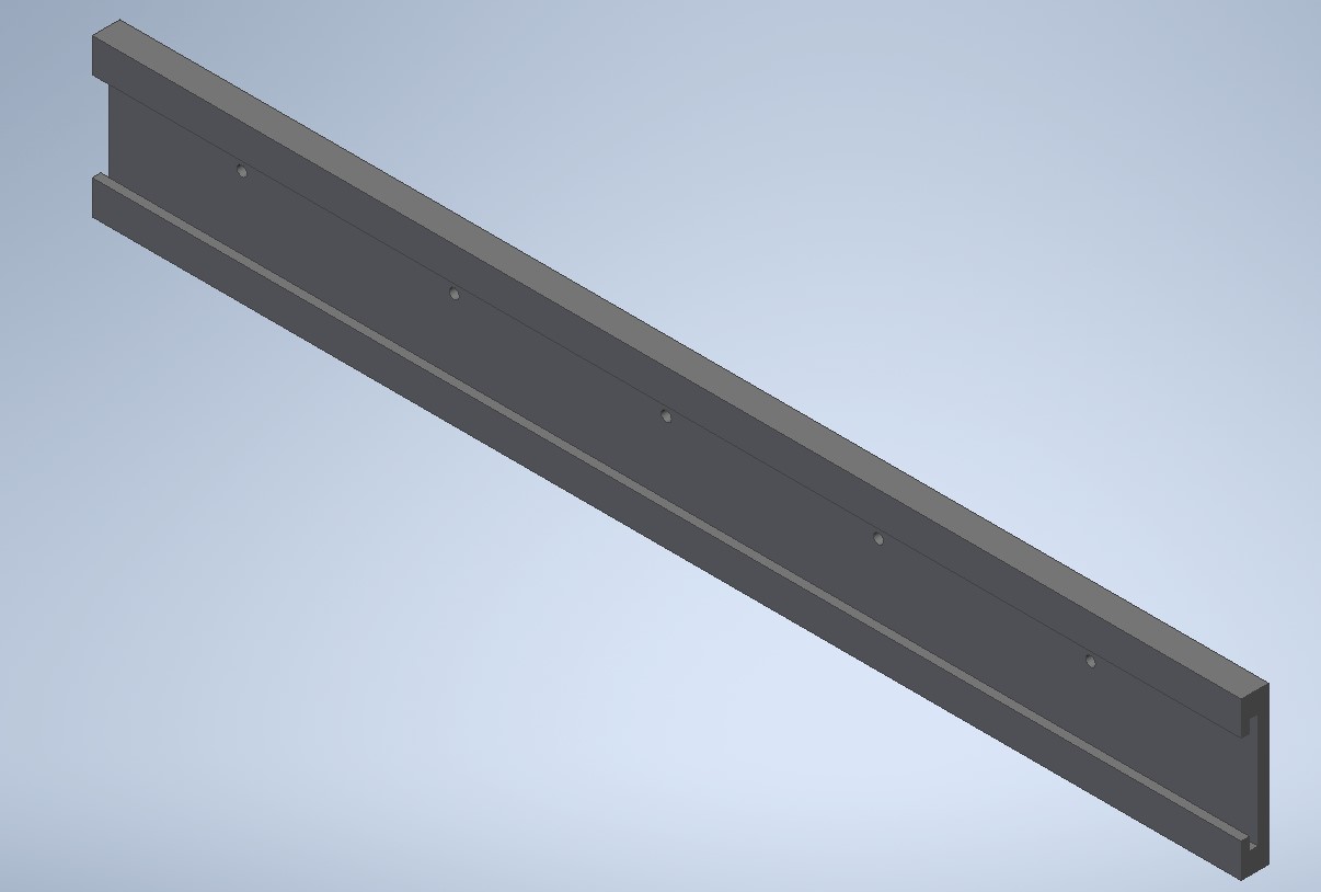
After talking with Dan about the design, we came up with a plan to handle the areas of concern I highlighted above. To handle turning the gears, he thought from the drawing the user would basically use their thumb to turn the gears from the back one. I hadn't thought about this, and at least tentatively will try that method since I can always design and print a knob if it doesn't work well. For the rail, the method I was thinking of turned out to be the simplest and that would consist of adding a protrusion on the lower part of the rail to prevent it from lifting off the ball bearing. I would then need to screw or glue on an endcap to then prevent the rail from sliding off the bearings entirely. During the consultation, I also realized that I needed to design an additional part to make sure that the wafer alignments pads did not come off of the wafer holder as at the moment there is nothing from preventing upward motion. Both the updated rail as well as the new pad holders are below. We didn't discuss anything about the electronics, which is fine because I have a lot of space to fit them into later. Dan however, did show me a scrap device that was set to be disposed of with a very nice aluminum bottom plate. It fit the dimensions I was planning for my base, so I grabbed it and will start machining it soon!

Printing Parts (Additive Manufacturing Technique)
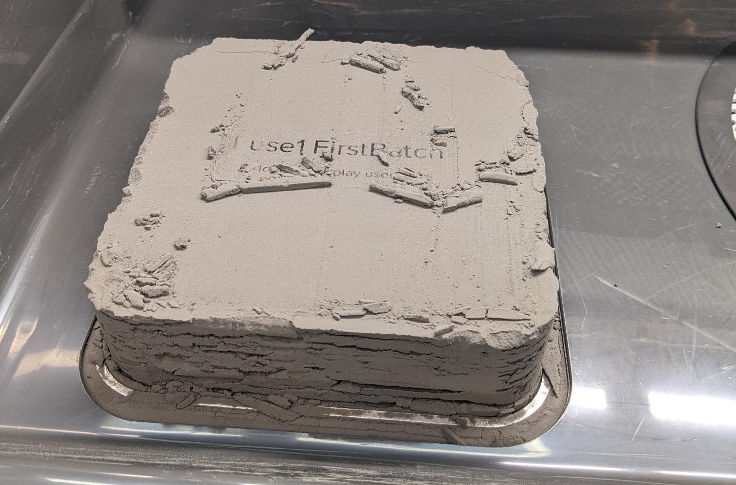
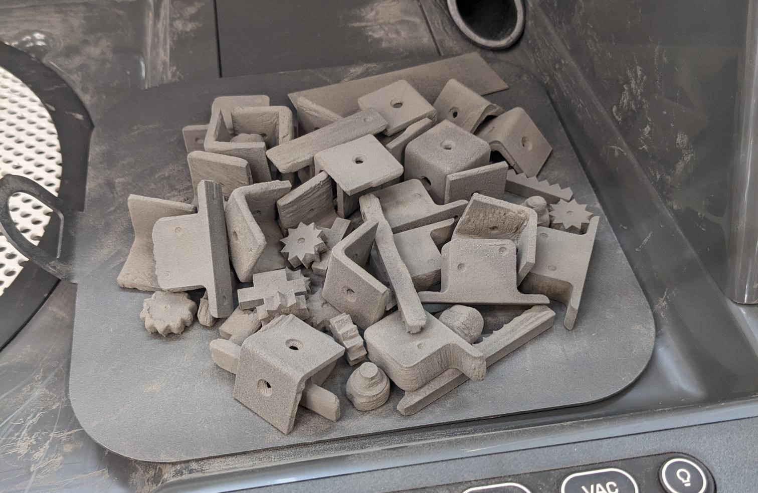
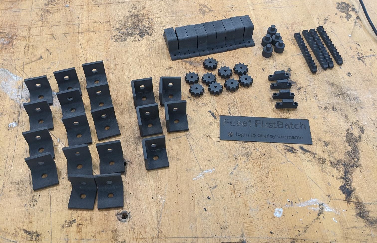
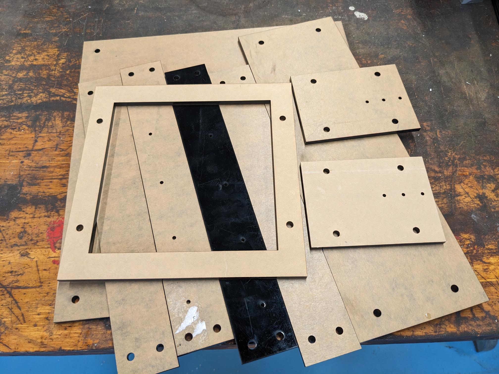
There are a number of parts in my design that are great candidates for 3D printing, largely because the print time will be much faster than machining them and they do not require a high amount of strength. The first batch of parts I printed were on the Fuse 1+ SLS printer, and consisted of a wide variety of parts. I included all of the brackets, the gears, the gear mounts, plate standoffs, the linear slides, and the alignment contact pads for the 6in wafer plate. The build area was pretty packed, but the Formlabs software did a great job optimizing the layout of the parts and was super easy to use. The print would take about 3 hours plus cooling time, so I started it on a Tuesday evening and came in before class on Wednesday to unload and finish my parts. I cleaned them up pretty well in the hood next to the fuse to recover as much powder as possible, but then bead blasted them with fine glass pellets to get rid of any remaining nylon. The process did take a bit of time, but it was very simple and the parts came out great. I had done a bunch of traditional 3D printing before with PLA, but I am a huge fan of the SLS process so I may be printing a few more parts on the Fuse down the line if I need them.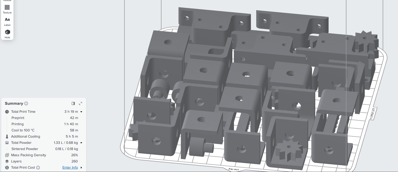
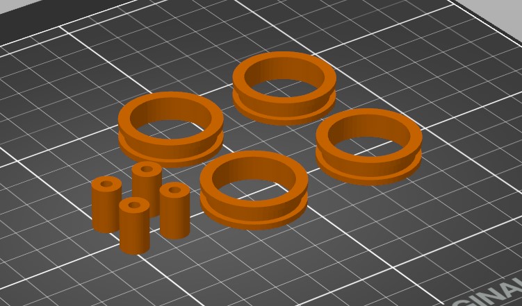
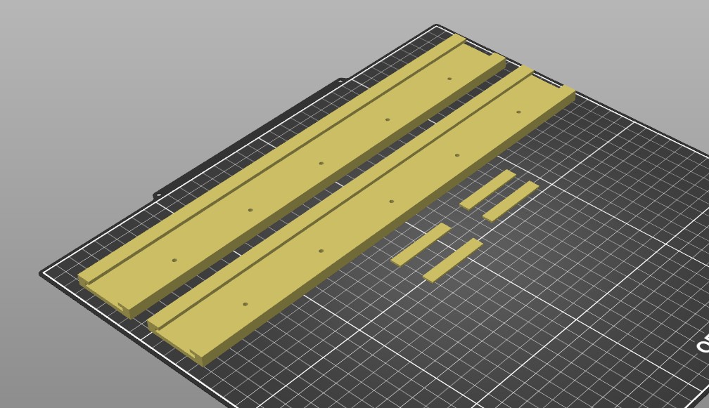
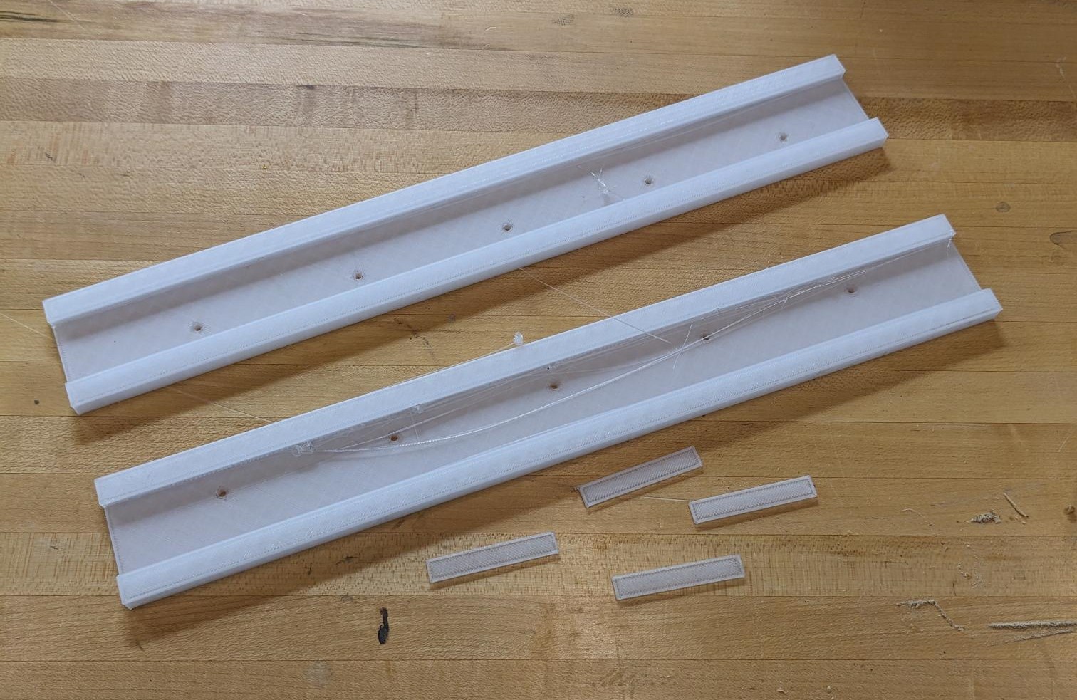
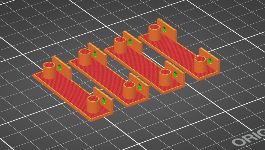
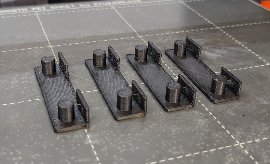
Aside from the Fuse, I did also make use of the Prusa printers in the CBA shop. I ran a very quick job on an MK4S to print the parts that would go on the inside and outside of the ball bearings. This was intended to primarily check the fit and the dimensions, but they turned out pretty well so unless I have to I am not going to re-print them. The second job I ran on the Prusas was the ball bearing rail which initially gave me a bit of a challenge because of the footprint needed. This could not be made in the Fuse since the print volume was not big enough, nor could it be made on an MK4S. Luckily, it just fit into the Prusa XL print bed so I had to modify my Prusa Slicer software to make sure I was using the correct printer. I set up a job to run one evening and came in the next day to remove and clean my parts. The last 3D printing job I did was the wafer alignment pad holder that I realized I needed during my consultation. This was a very simple piece that will seat into the 6in wafer frame, and will be screwed into the side of the frame once it is place over the pads. I needed 4 of them for each cardinal direction on my wafer frame, but they were pretty small so the job was easy to run. All of the Prusa prints were at 15% infill and are made out of PETG (bearing parts and the rail) or PLA (alignment pad holder). I enabled supports because I did have some recessed features on each of the prints.

Laser Cutting Acrylic Parts (Subtractive Manufacturing Technique)
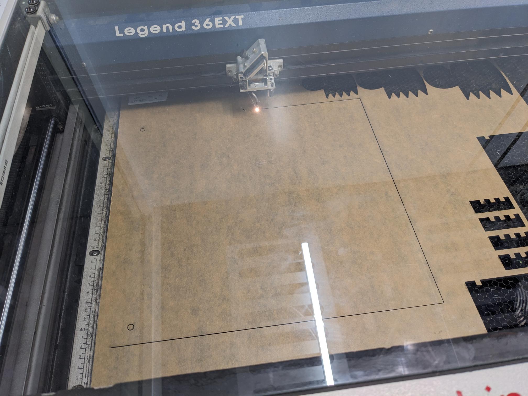
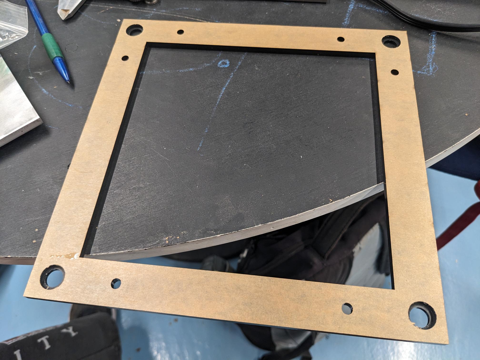
I decided to form most of my structural elements out of acrylic because it is cheap, easy to shape, and strong enough for my application. None of these pieces required any special processing methods or techniques, so I laser cut most of them on the XTool. I exported all of the sketches as DXFs, loaded the pieces of stock, and used the wonderfully simple interface to set up my cutting paths. I specified the material was ~6mm (1/4in) in the software and it handled all of the laser settings automatically. I did cut a quick test structure to make sure the settings would get through my stock and that was successful without any changes. With that test complete, I just had to sequentially put in my stock and cut all the pieces I needed. I did need to run the larger piece on the Epilog since it was too large for the XTool, but in following the prompts for using 1/4in acrylic the cut came out great as well! After running my initial laser cutting jobs, I looked into acrylic UV resistance because I wasn't sure if I could use this material for my mask/magnet frame. As much as all plastics will eventually degrade in UV, acrylic is actually decently UV resistant which meant I was not worried about using a little bit of it underneath my UV light source. Worst case, this part could be replaced easily and that would not be expensive either cost or time wise. This part also is designed to accommodate 1/4in thick 1/8in diameter magnets to hold the mask in place, which were ordered off of Amazon.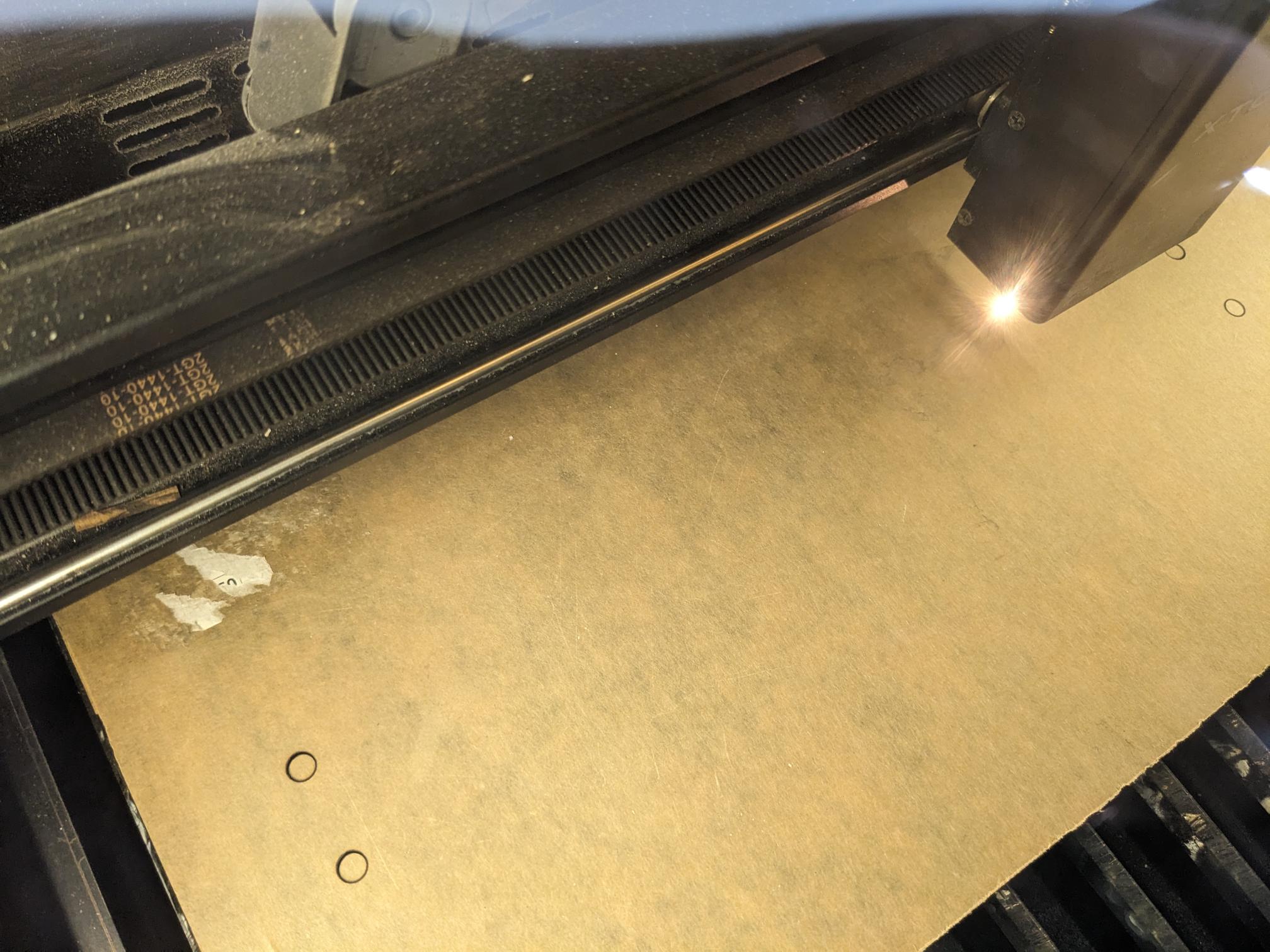
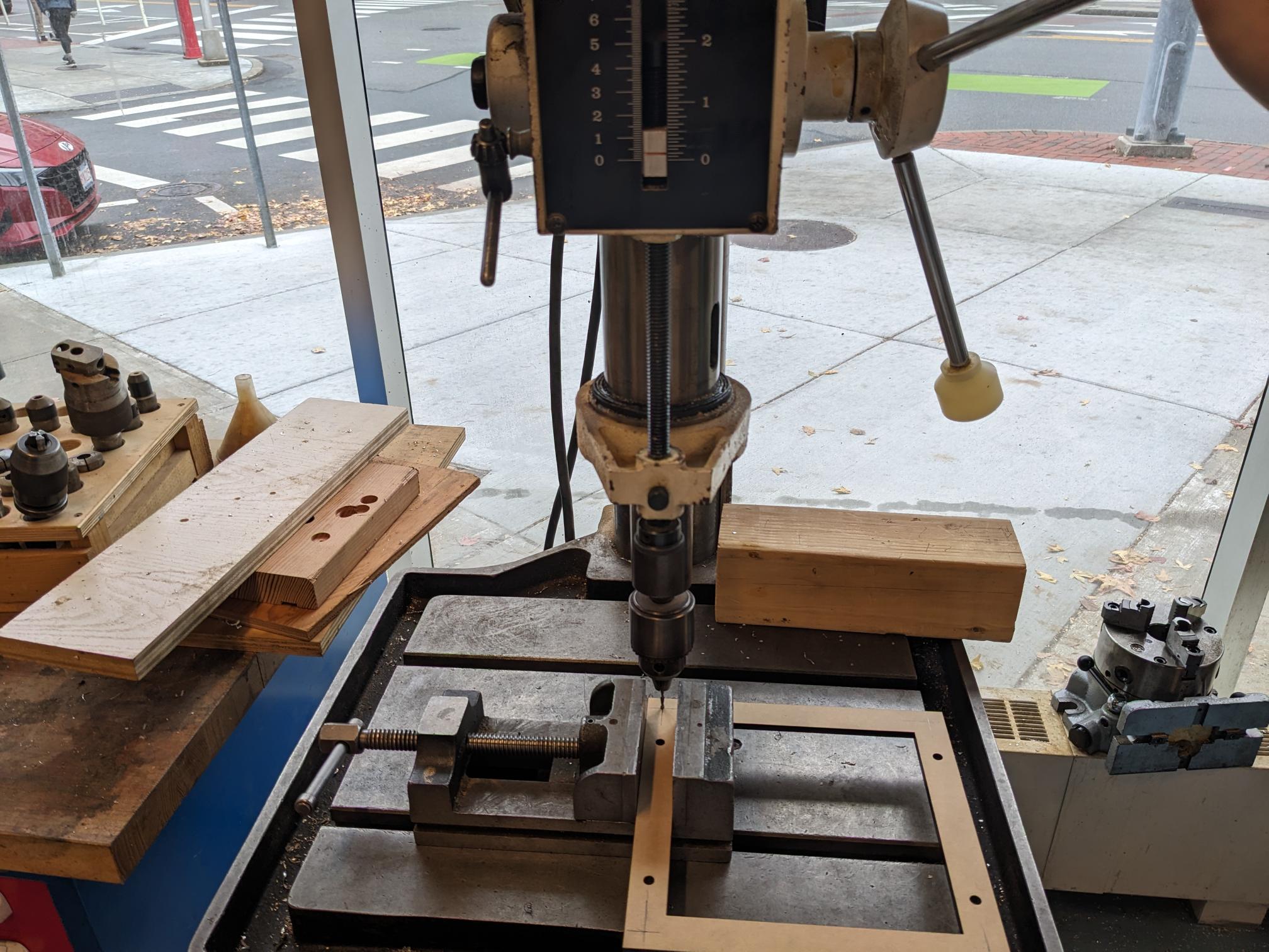
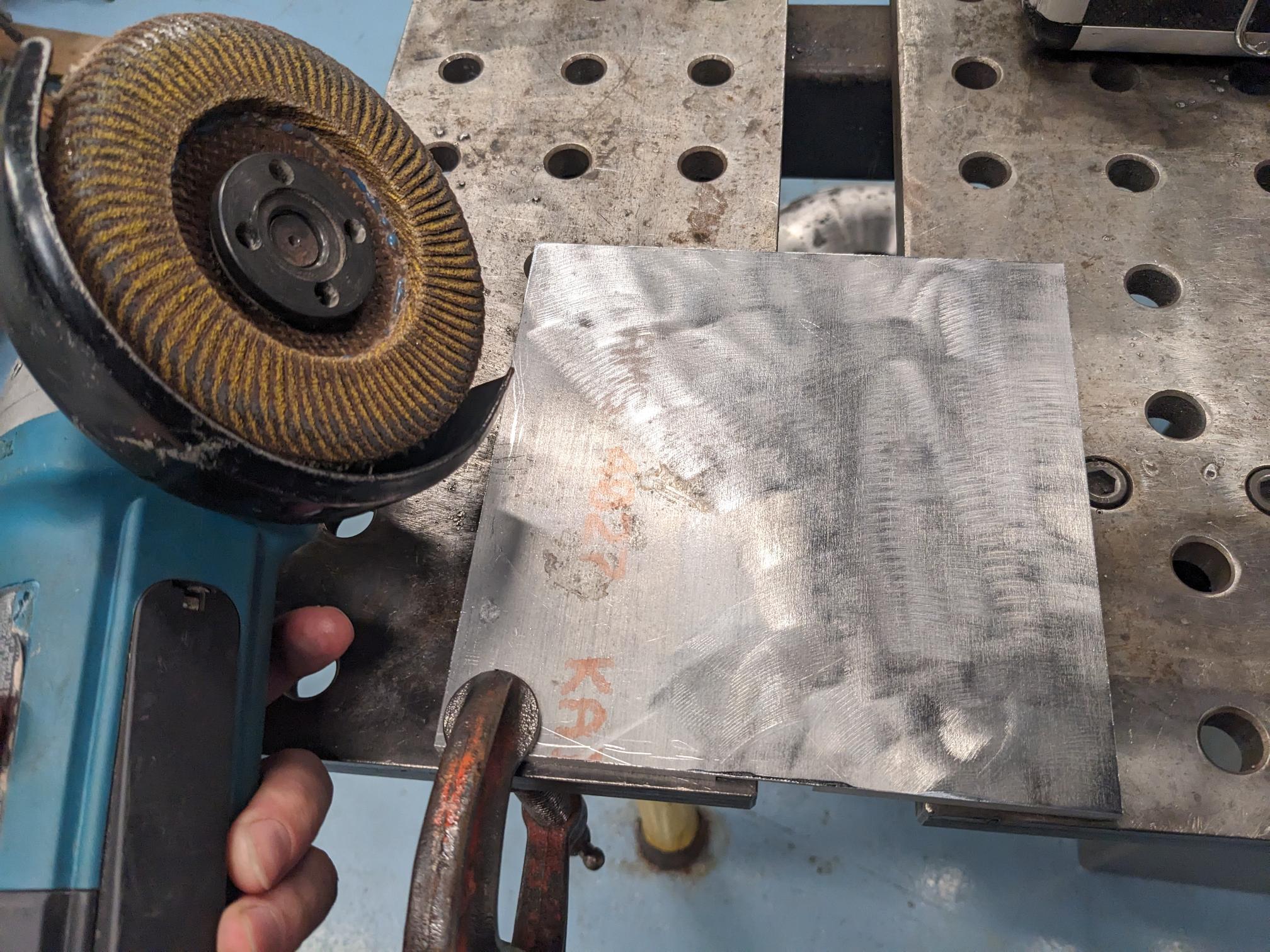
I did need to drill some holes 1/8in into the corners of the mask frame but not all the way through so it can sit on the standoffs I designed. I did this manually by marking out where I wanted them to go and using the depth markers on the drill press to make sure I was going to the right depth. Charlotte at the hobby shop suggested that I use pilot holes to prevent cracking my stock, so I started with 1/8in, then stepped up to 1/4in, and finally went with 1/2in. I also used flat endmills because I wanted a flat profile, and tested the drilling on a scrap piece before committing my part. Unfortunately, I made a bit of a assumption that did not work in my favor. I had just finished up the 1/2in in cut on the test piece, meaning the step-up drilling was working great, and I tested the fit on my standoffs. It was much tighter than I was looking for, so I figured I could just use a slightly larger endmill like 9/16in. The 9/16in worked great size wise, but I did not think that there would such a difference between 9/16in and 1/2in when actually milling my acrylic. Sadly, there was a moment during drilling where the endmill skipped while cutting and it shattered one of the corners of my frame.
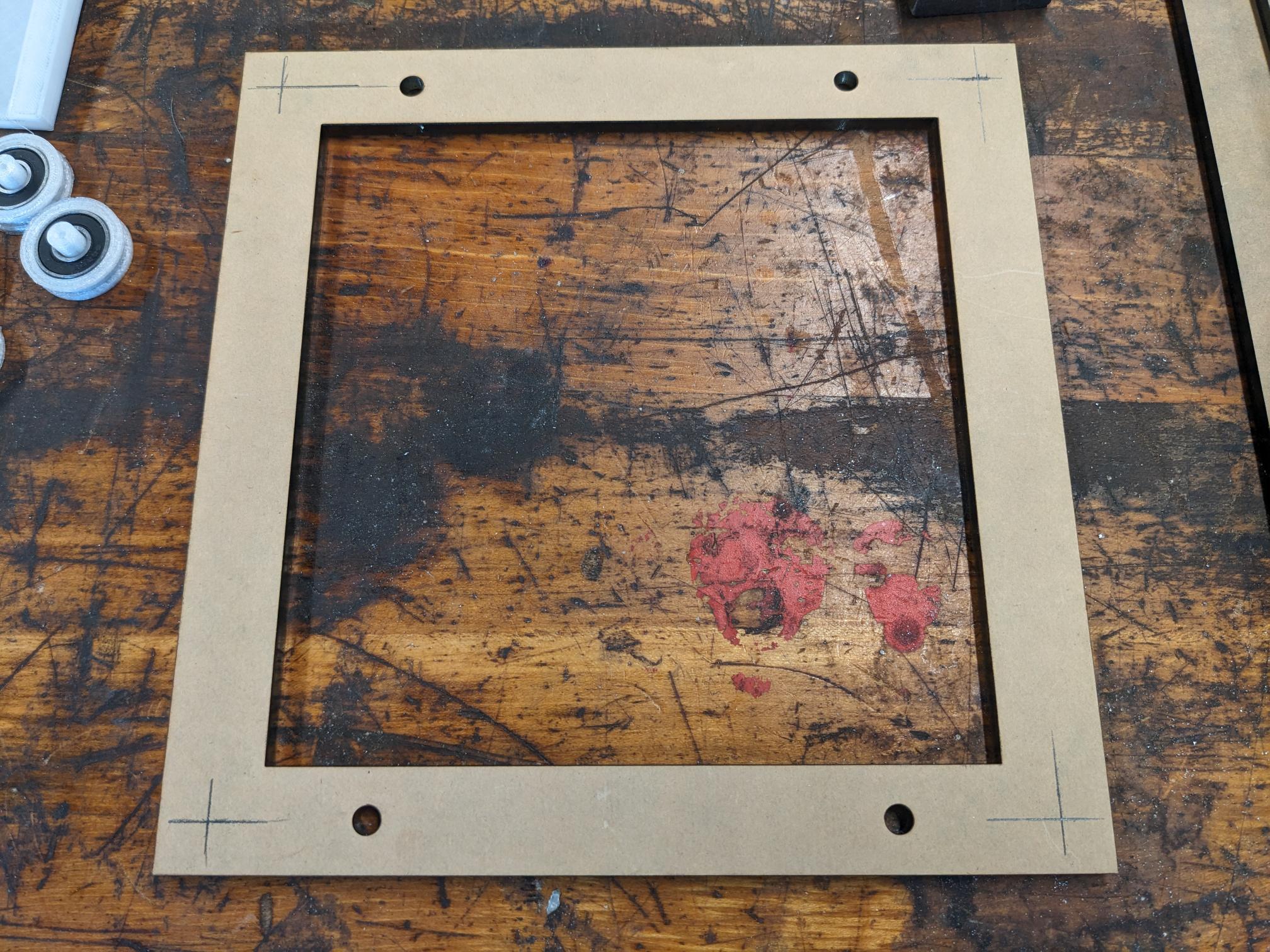
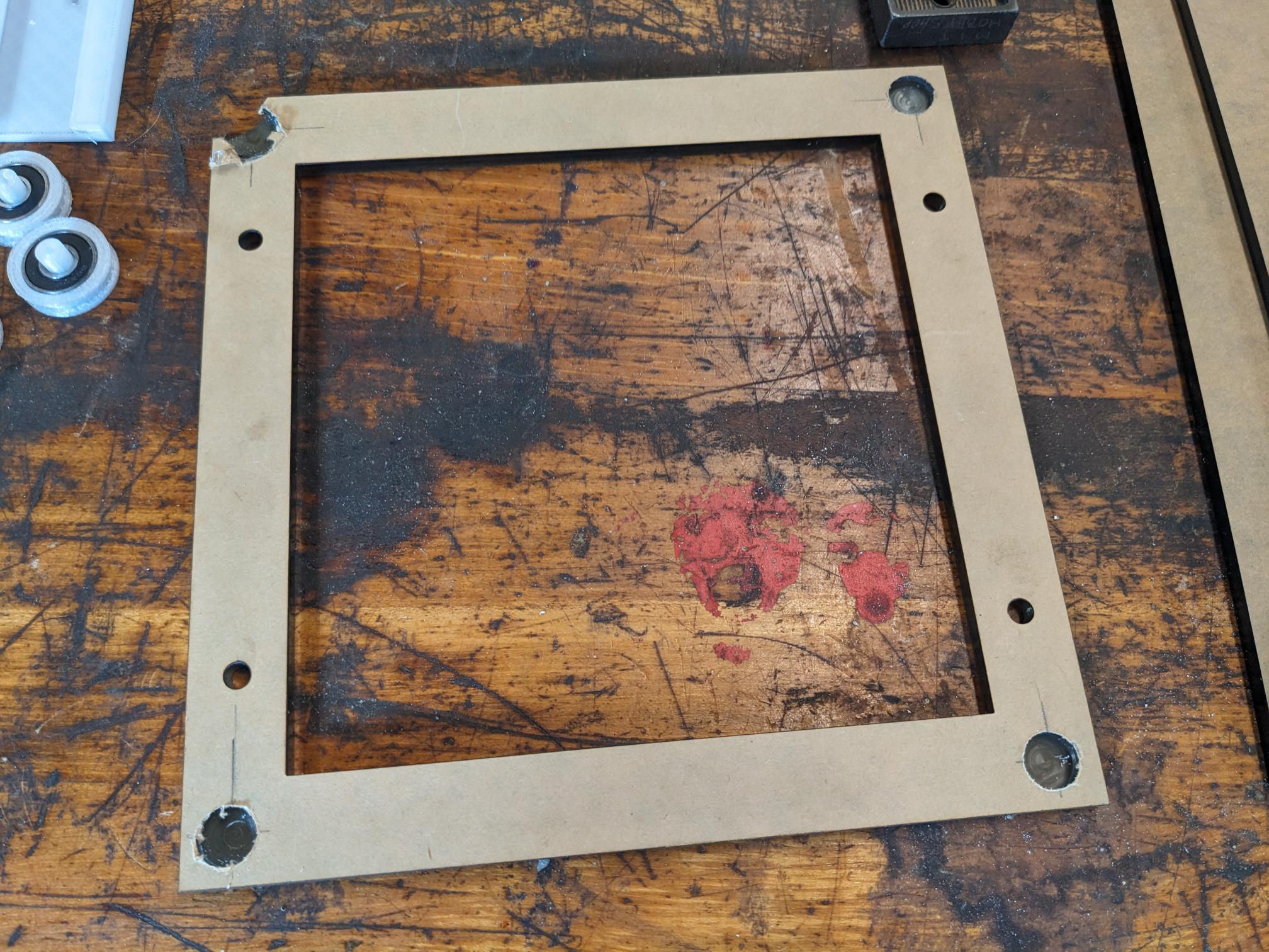
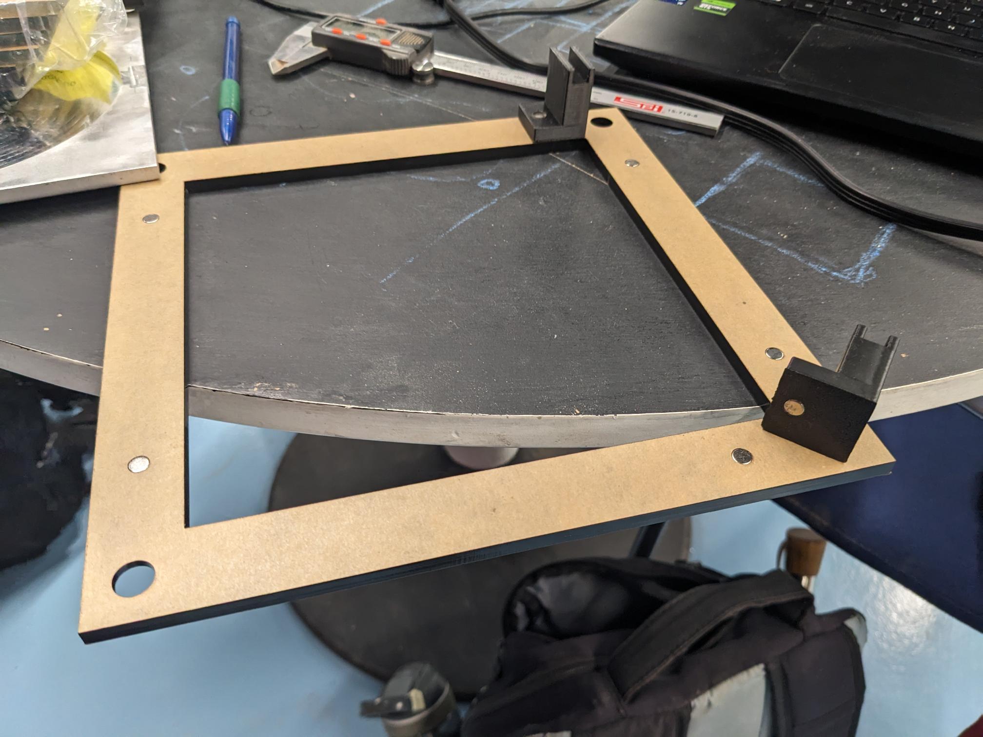
Luckily, I had plenty of time and scrap stock left over to make another one. I also made some changes to the design based on some learnings I gained in the assembly process. I added the pilot holes to the corners so I would just have to drill with the 9/16in endmill, I shrank the diameter of the magnet holes to .225in to make sure there was a snug fit, and I added two more magnet holes to accommodate a 3D printed support for the light box. Details on this support and why it was needed are discussed in the assembly section of this page. I ended up cutting out two frames just in case I broke one of them again, but I didn't even need to use the second one because the addition of the pilot holes on the laser cutter worked very well!
Water Jet Cutting Aluminum Parts (Subtractive Manufacturing Technique)
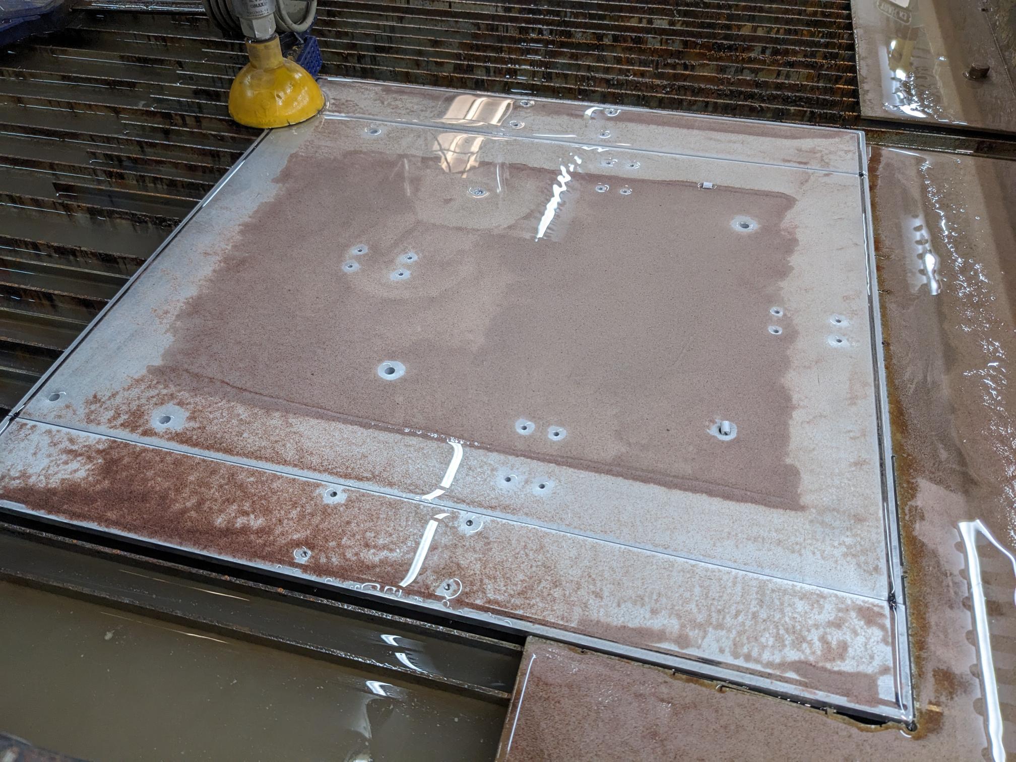
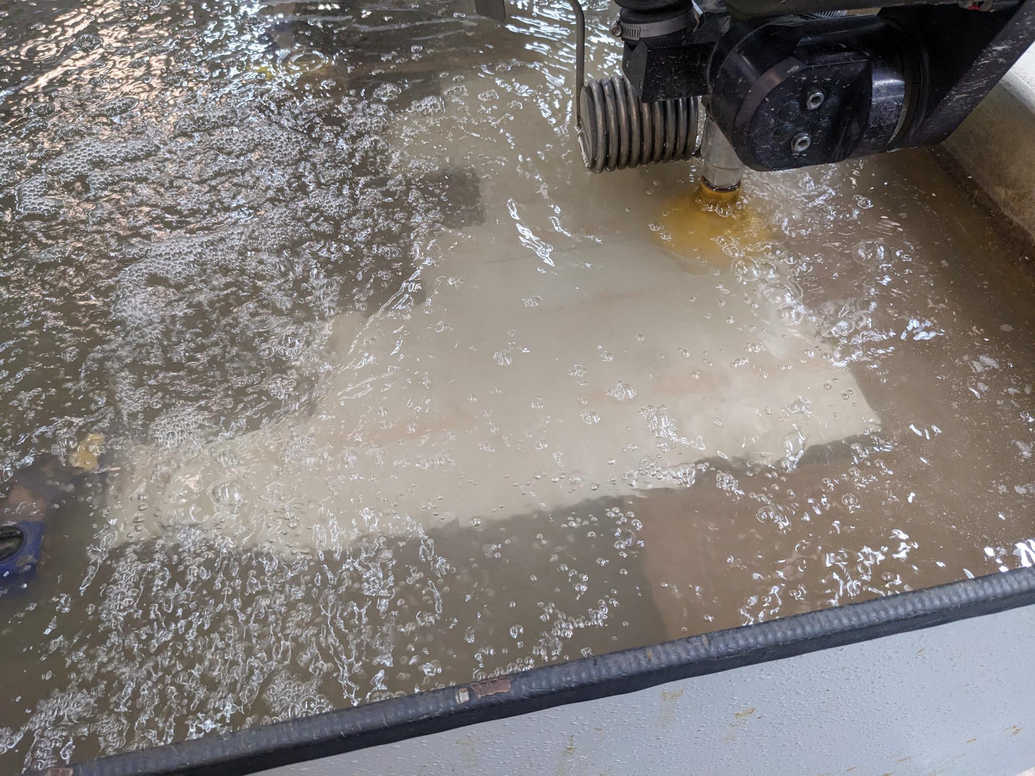
I chose to make my base plate out of aluminum so that it would be more sturdy than acrylic when it comes to supporting everything mounted to it. There are also a few pockets that would be cut into it that I want to be rigid and they would be exposed to UV light, so it made sense to go with a metal. Luckily, Dan showed me a 1/4in thick plate that was about to be scrapped that nearly fit my dimensions perfectly. We determined it would be best to make the initial cuts on the water jet first to get the footprint and any through holes needed, before going to milling. I exported a DXF of the back side of the plate so only the through holes and outside footprint would be captured, and then set up the job on the water jet. I had water jet a few parts before, but this was very simple to start. We clamped it down outside the expected path of the nozzle, set the file, selected a starting position, and zeroed the XYZ coordinates of the tool. Then it ran really smoothly and clean up at the end was simple enough!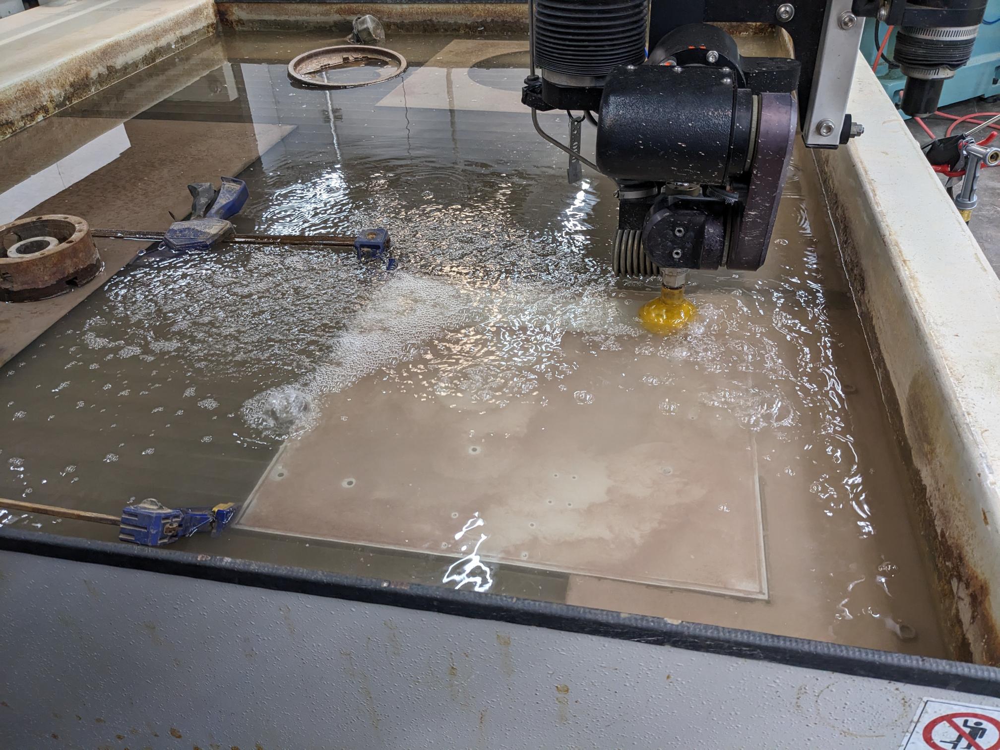
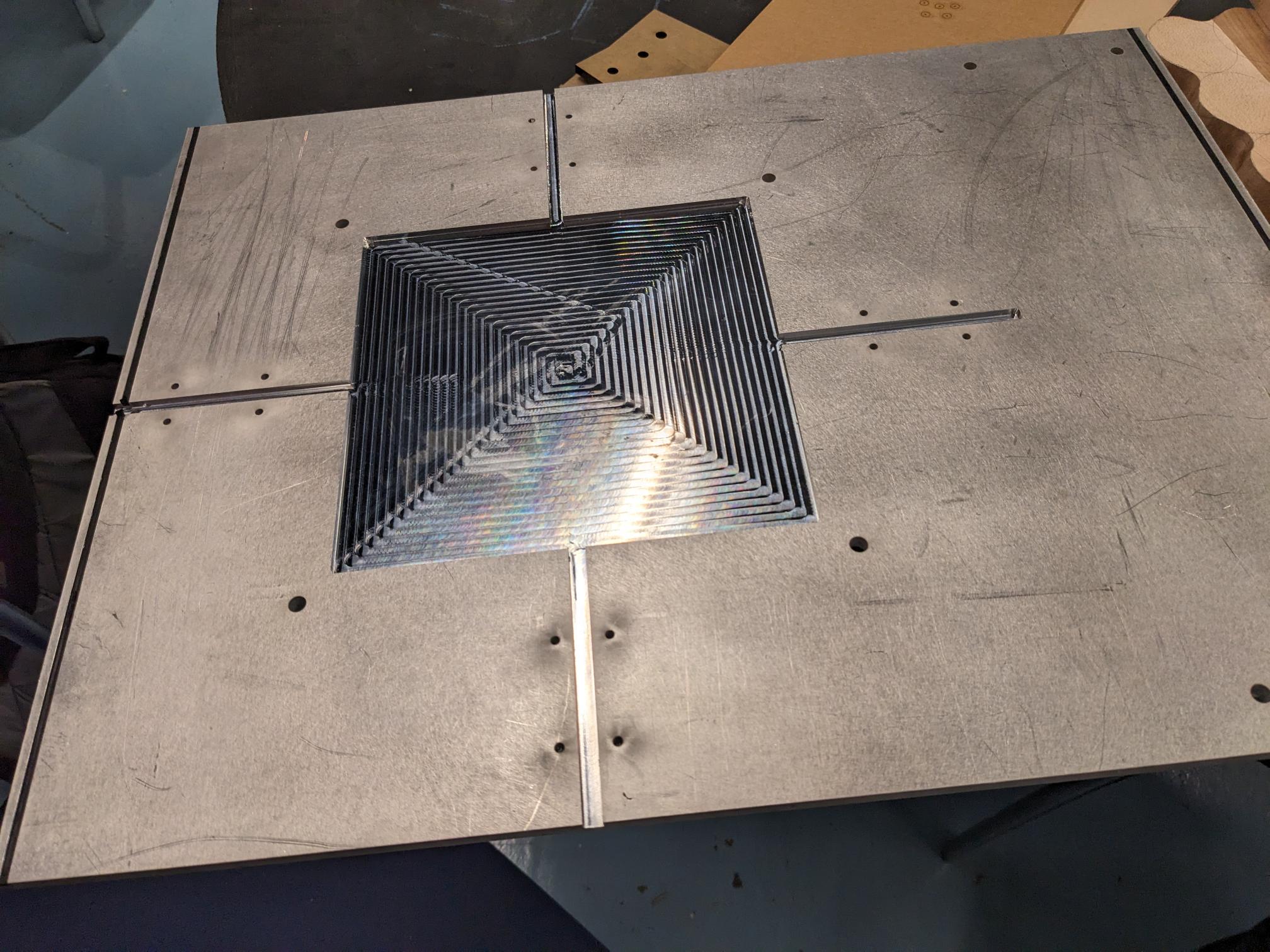
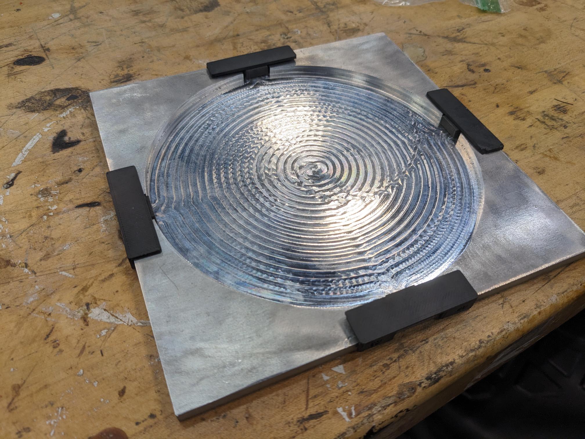
I also chose to make the 6in wafer holder out of aluminum mostly because it is very common to use for wafer chucks in cleanrooms, so I figured I might as well keep that consistent. That did mean I needed to cut out the footprint of the piece, so I found a large enough stock piece in a scrap pile and took it to the water jet to cut out the square footprint. This was an even simpler piece to cut because it was just a 7in x 7in square.
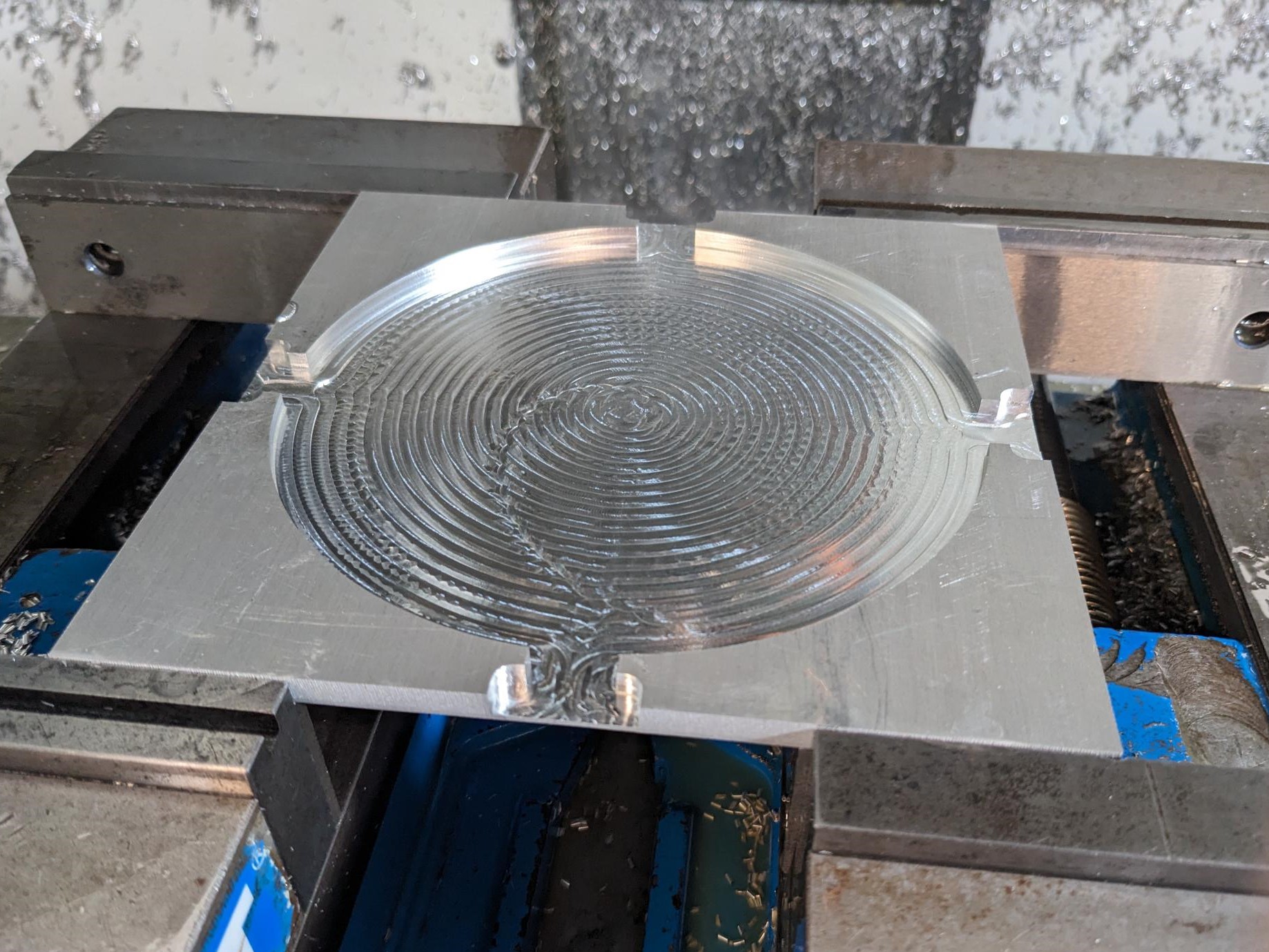
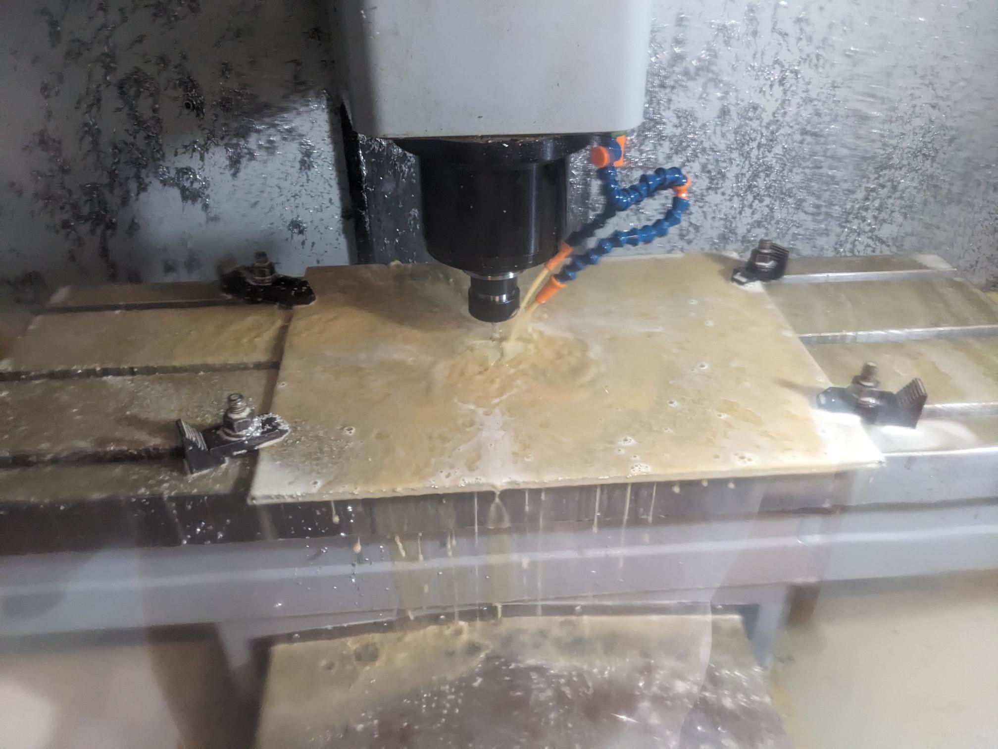
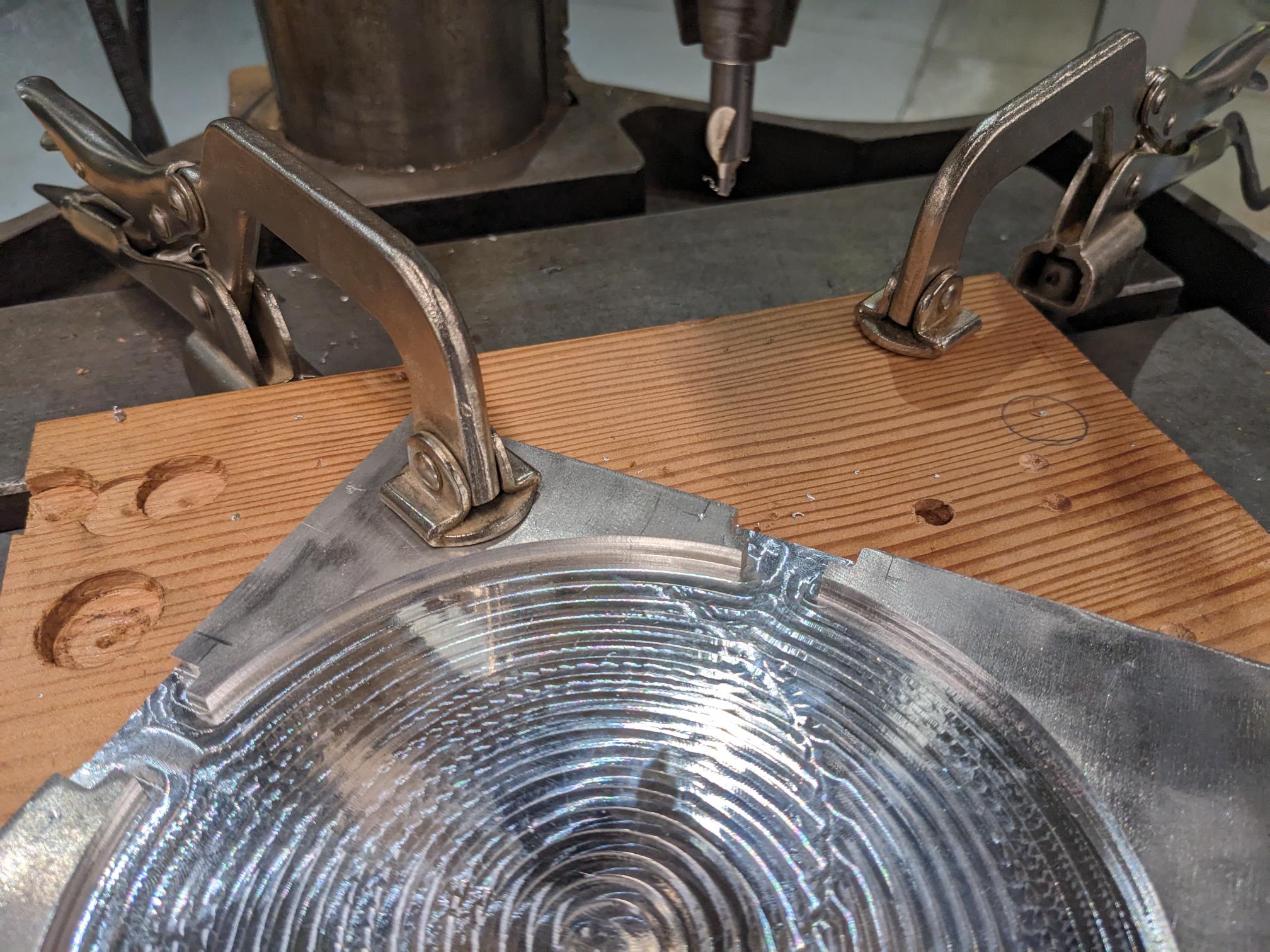
CNC Milling Aluminum Parts (Subtractive Manufacturing Technique)
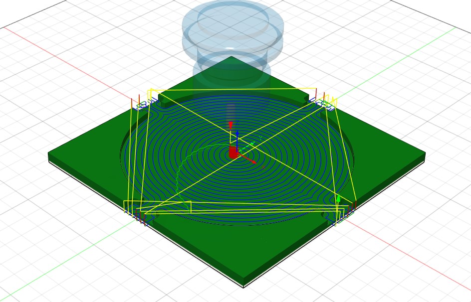
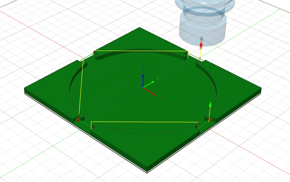
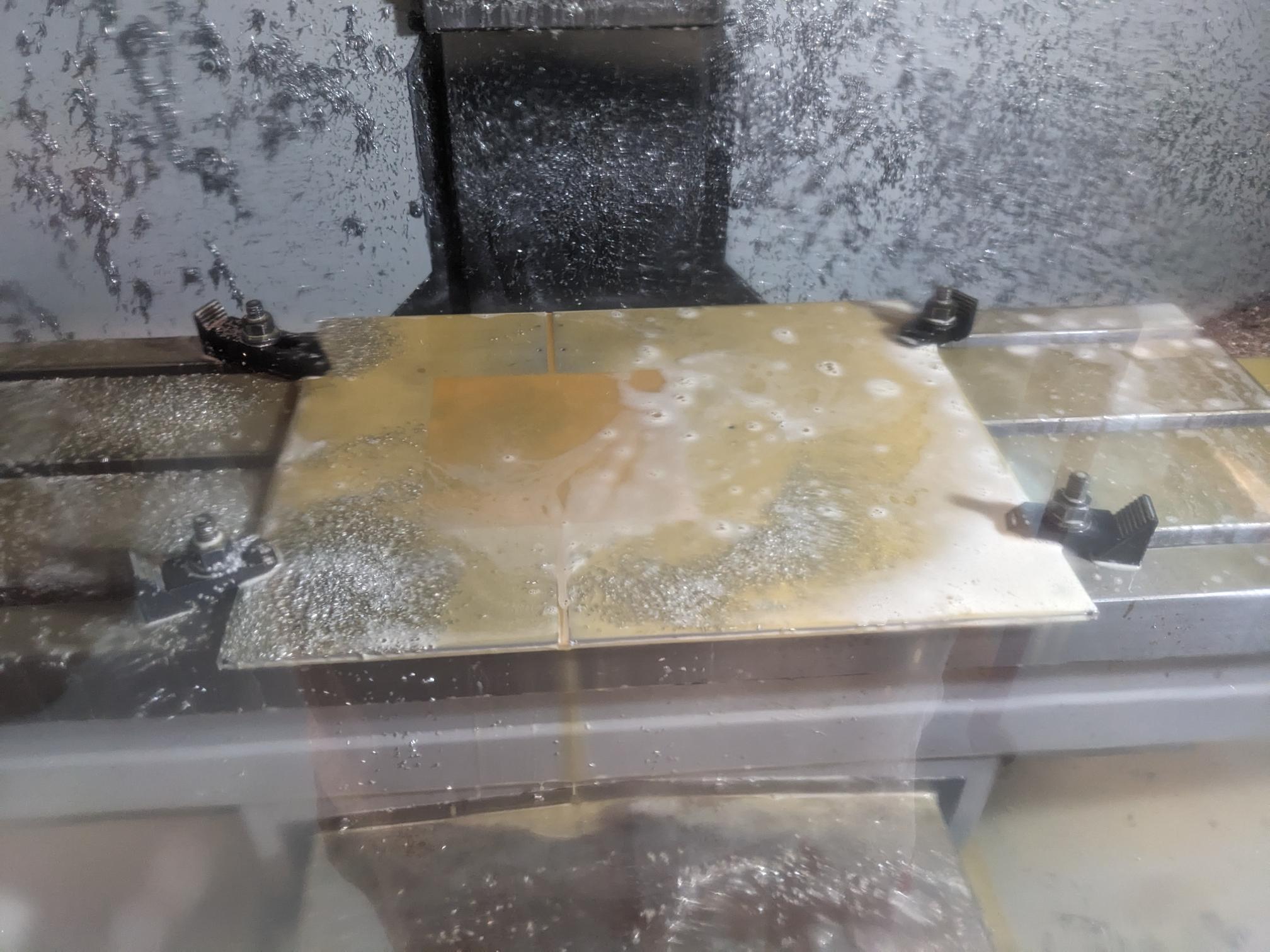
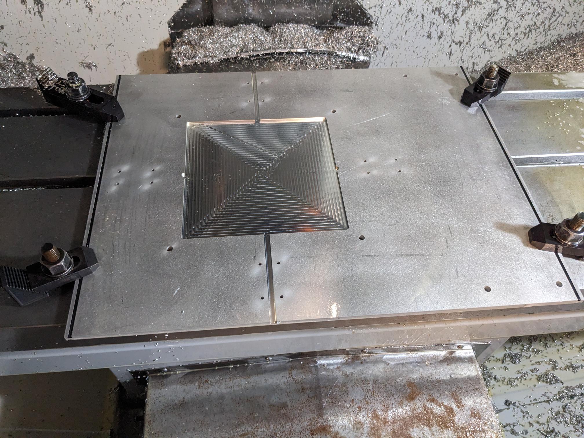
Following the through and frame cuts for my aluminum parts, I then needed to get the surface profiles cut into them. In both cases, there was essentially only one pocket that would be cut a consistent distance into the stock. As such, I set both jobs up to make use of a 1/4in flat endmill to handle the removal of most of my material, followed by a 1/8in flat endmill with rest machining enabled to trim the corners a little bit better. I made sure that my stock sizes were set to the footprints I had already cut (the wafer frame stock was 1/4in thick instead of 5/16in which is fine) and I set the center axis to match the axis of the Haas. I made use of the Feeds and Speeds Wizard to select the proper RPM and feedrate based on the endmills I was using and then exported the G-code with the Haas Pre-NGC post processor. Some important settings to make note of are as follows; 1/4in endmill had speed = 10k RPM and feedrate = 71.88 in/min with a step down of .1in and a step over of .15in for both cut jobs. For the 1/8in tool, the base plate had a bit more to cut so I did not use as fine of a stepover as the wafer frame. As such the parameters ended up being speed = 10k RPM for both, feedrate = 25.8 in/min for the wafer frame and 24.33 in/min for the base, a step down of .05in for the frame and .1in for the base, and a step over of .0375in for the frame and .0625in for the base.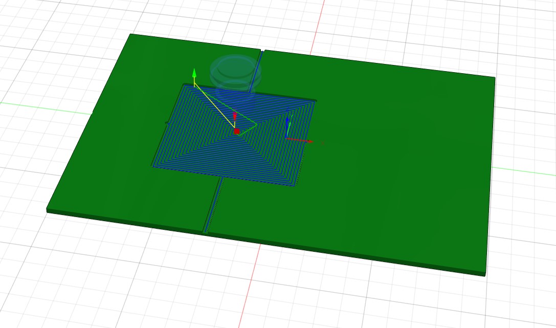
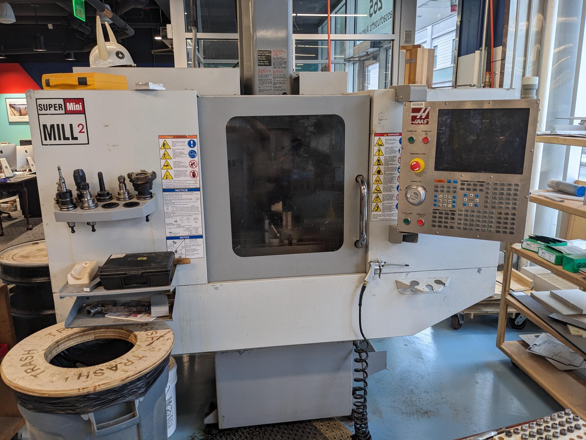
Initially I was going to cut these parts in the CBA shop on one of the ProtoTRAK mills, but in talking with Dan he made a passing comment about how it would be better to cut these parts on a more automated CNC tool. As it so happens, I have recently been spending a decent amount of time at the MIT Hobby Shop using their Haas Mini Mill 2 (which is by no means mini). I mentioned this and Dan actually suggested using that tool for these cuts which I then set about doing.
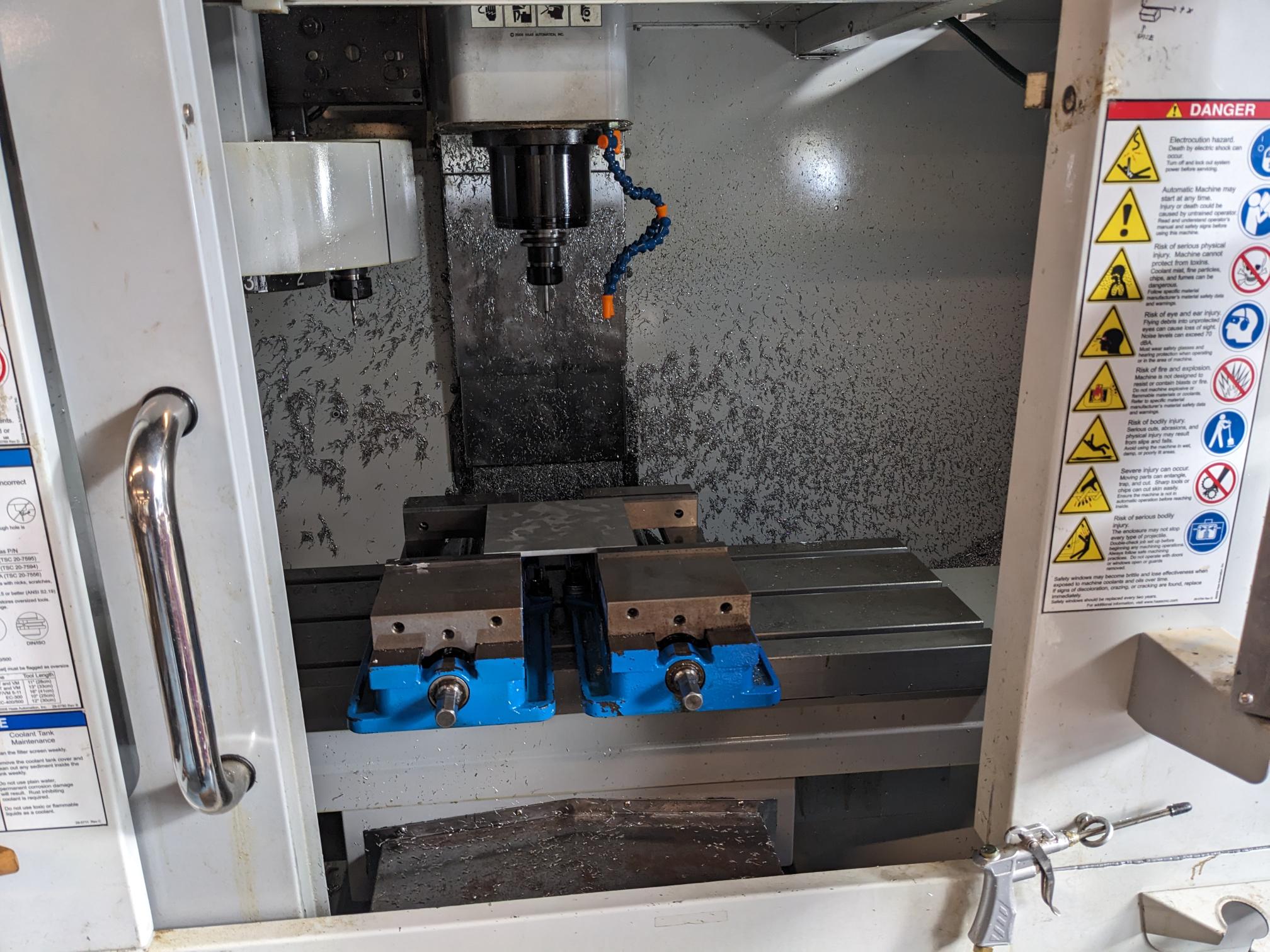
I started with the wafer frame since the base plate would require removing the vises that had already been set up and squared away to the cutting bed. I set it up in the vices and used an edge alignment tool to find the coordinates that correspond with the edge of my stock. Since I knew the exact size of my stock as well as the radius of the alignment tool, I could then zero my coordinates to where I had them in my design file.
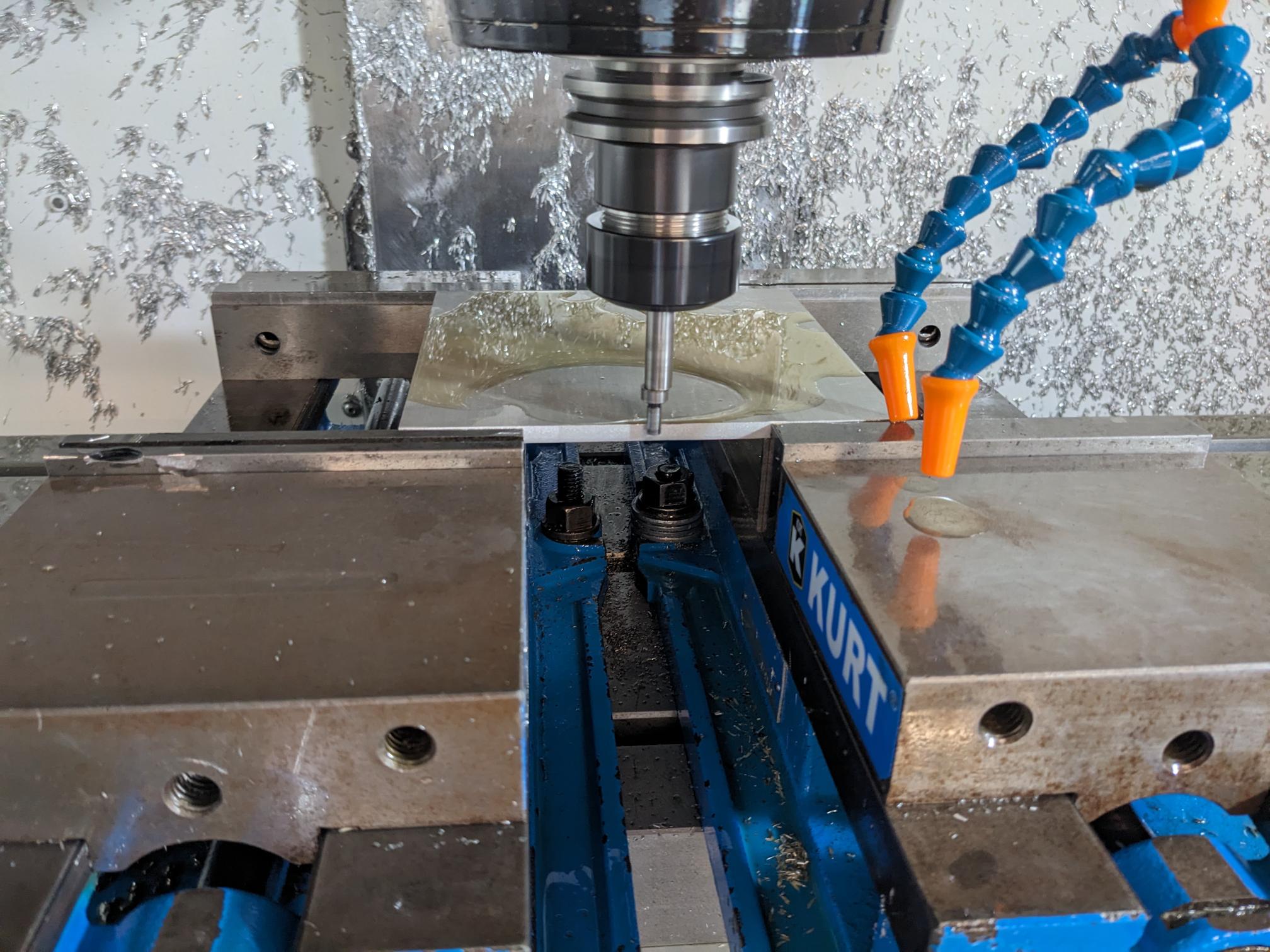
Running both cuts was super simple, the first job took about 20min to complete and the touch up with the 1/8in end mill took only a few minutes. The difference in the resulting corners is actually quite noticeable when trying to look for it (1/4in cut is on the left, 1/8in cut is on the right). There is a very slight texture that can be felt from the 1/4in cut, so I think that if I were actually trying to get one of these plates to be as precise as possible I would significantly lower the stepover distance to make sure I get a really flat cut for the wafer to seat perfectly on.
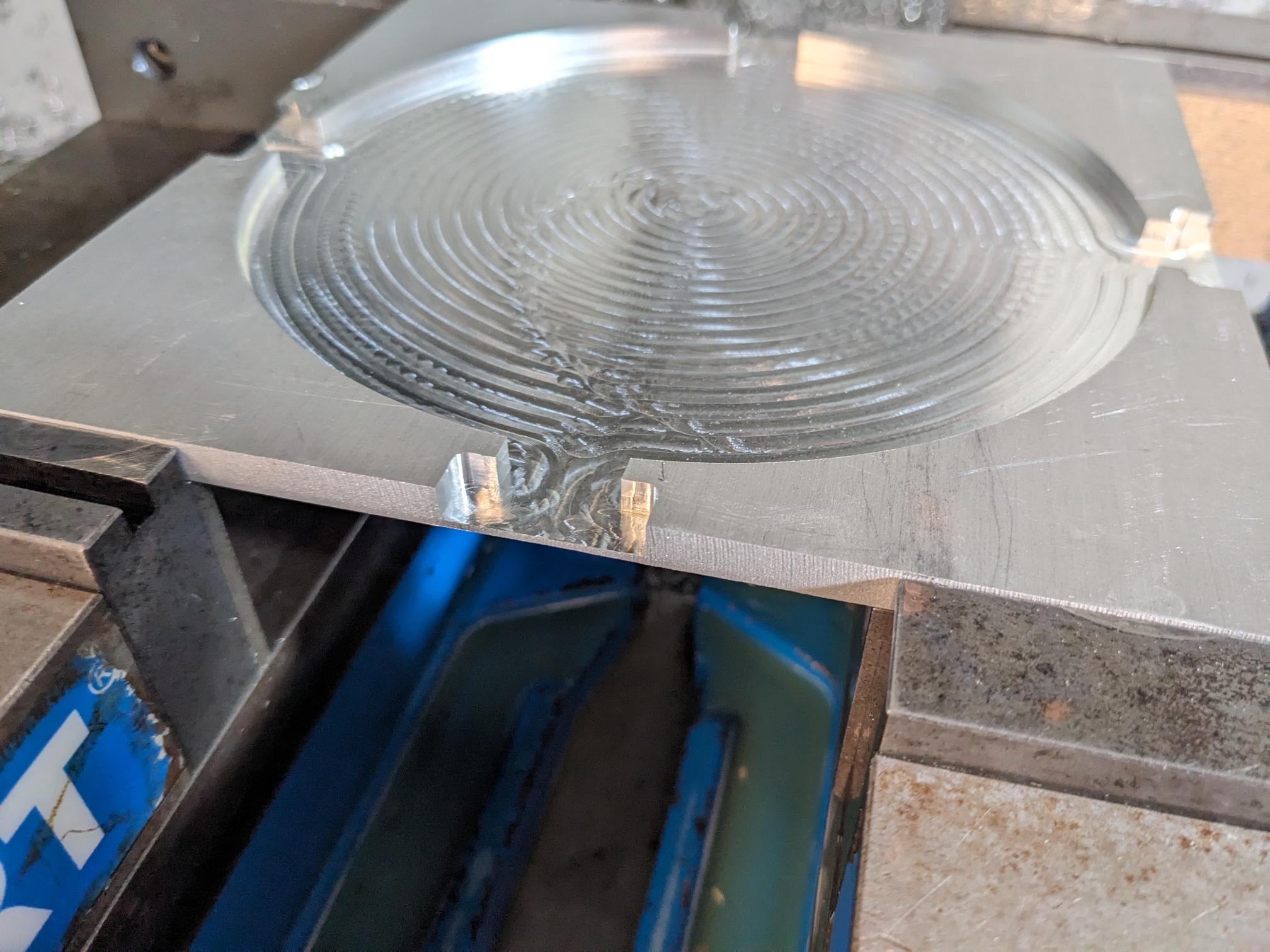
On a bit of a side note, I had never actually polished metal before so I looked into what type of techniques are usually used. The most common techniques were rotary polishers and pastes that get manually rubbed into the material, of which the Hobby Shop did have rotary polishing equipment on hand. The equipment was also meant for steel and was a bit coarser of a grit than would be used for polishing, but I had fun learning about the equipment and giving a very light (and definitely not high quality) touch up to my wafer frame!
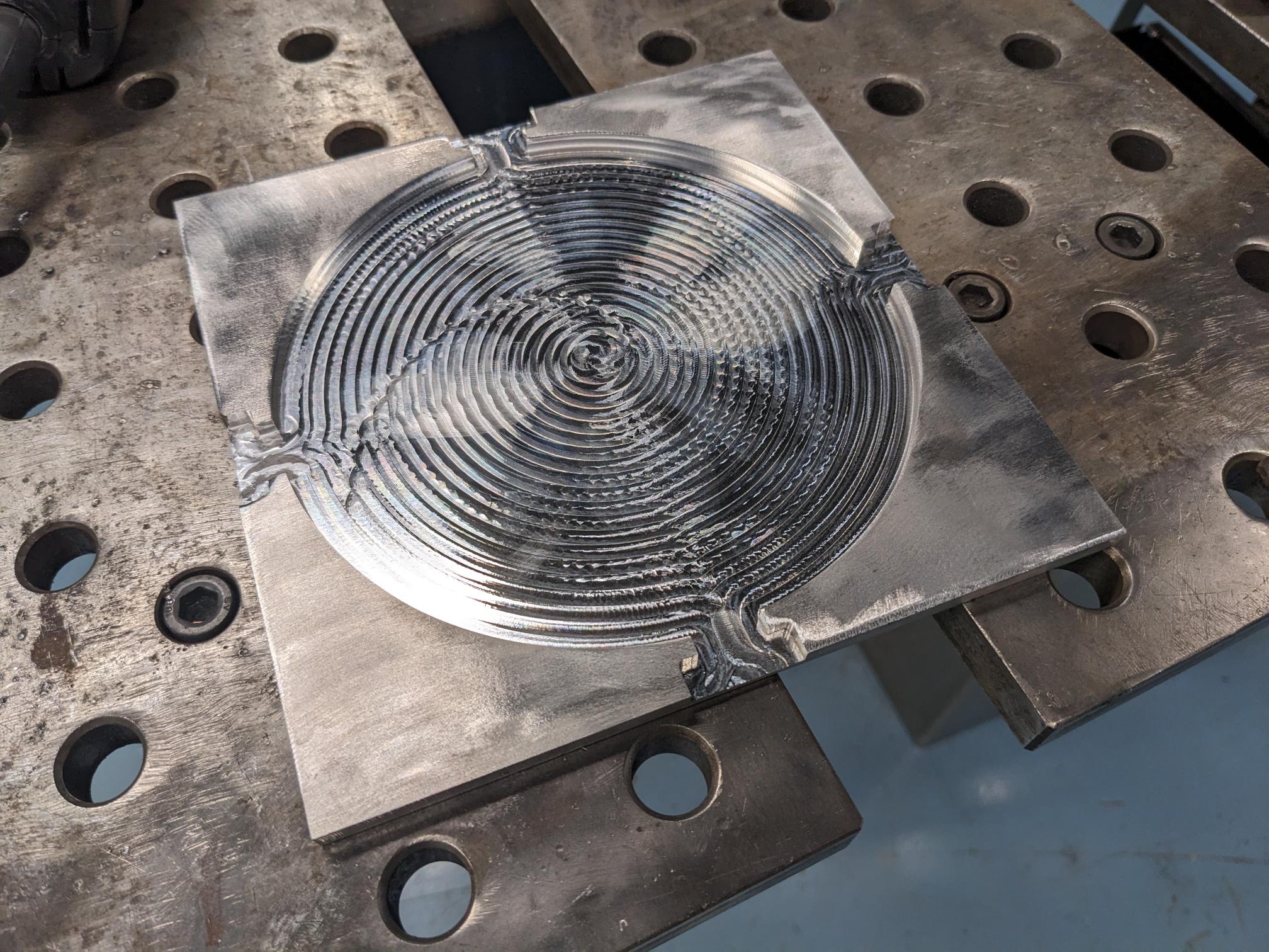
As for the base plate, this was a bit more tedious to set up since it was barely within the footprint the Haas could mill. I spent about 30min adjusting the edges so that it had a little bit of extra travel outside the entire cutting area, while also making sure it was squared up to the cutting bed. I had only used the Haas with vices up until this point, so I learned how to mount the parts with "toe clip" (I think is what they are called). Otherwise the process followed the same pattern as the wafer frame but I did not do any polishing on this piece.
Hand Finishing Aluminum Parts
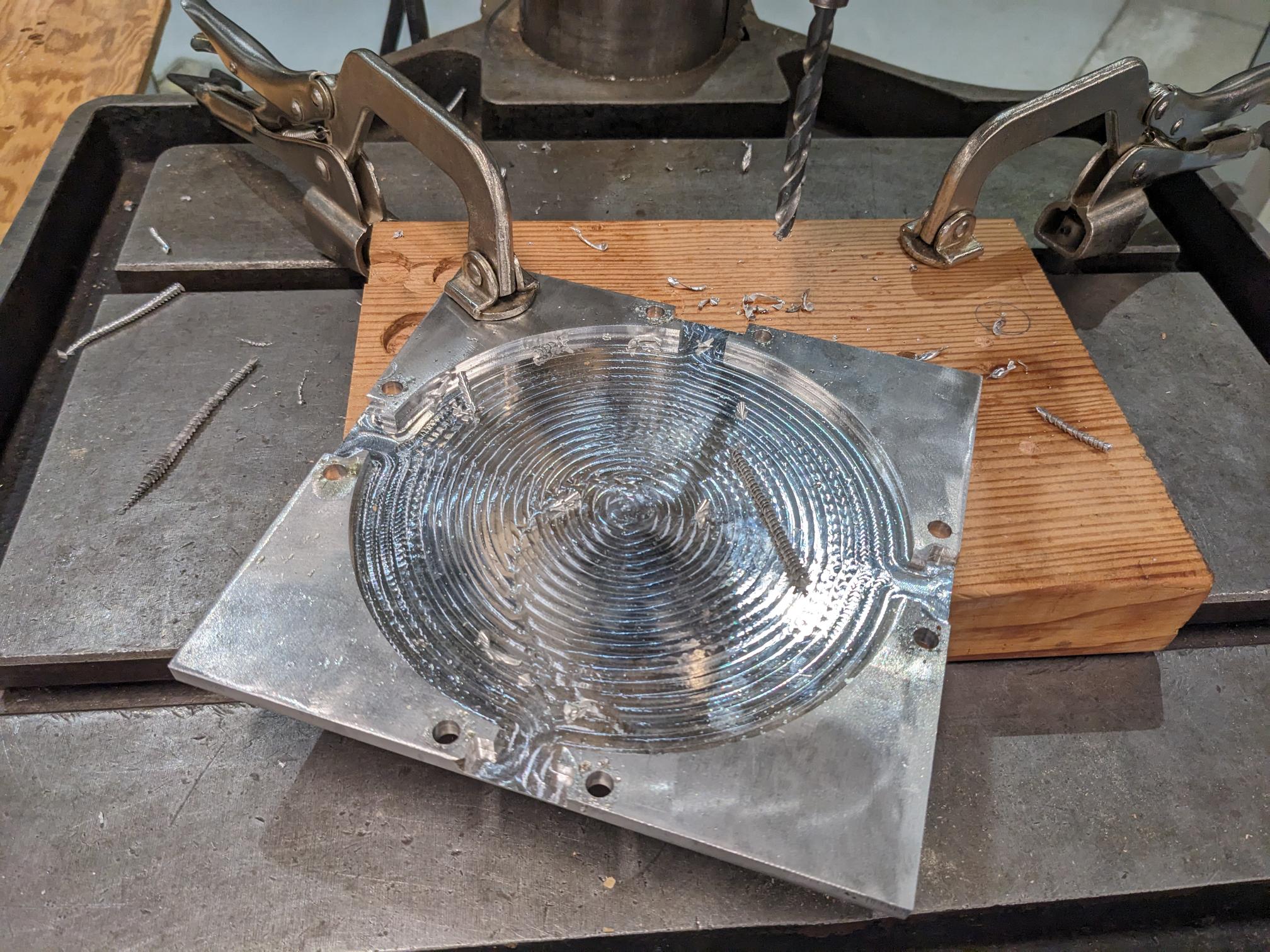
After making the parts on the Haas, there were a few more features I needed to make. The simplest of the two was the base plate because all I had to do for that was tap the screw holes for the sizes I had picked out. The acrylic pieces would be connected by 1/4-20 3/8in screws and the gear mounts would get 6-40 3/8in screws. There are setups that can handle tapping holes and automate the process, but I just did the holes in the base plate by hand and like so may of the other manual processes I found it to be mildly therapeutic.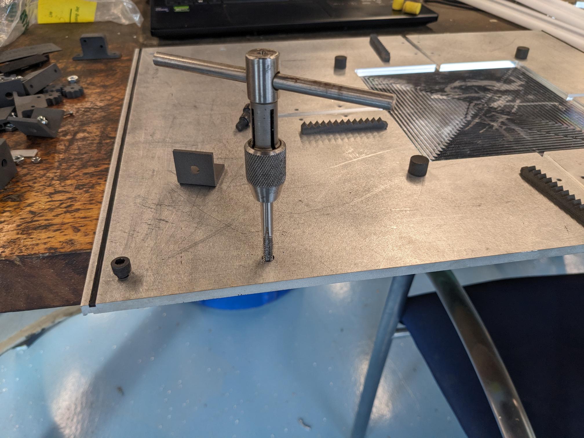
Unfortunately, in order to accommodate the alignment pad holder on the wafer frame, I needed to make 8 through holes and 8 tapped holes for screws. The through holes are not hard, I just marked out the location they needed to go, drilled an imprint with a centering bit, and then drilled the hole with a 1/4in bit. I do wish I had thought about this sooner because these could have been taken care of on the water jet which would have saved me some time. The screw holes would have been a lot more annoying though because I would have to mount the plate on its side in order to get at them. I would have liked to drill them, but I decided that I would skip this step in favor of making more progress on the overall project since this is a minor detail and actually doesn't have a large impact on the overall operation.
Electronics Design
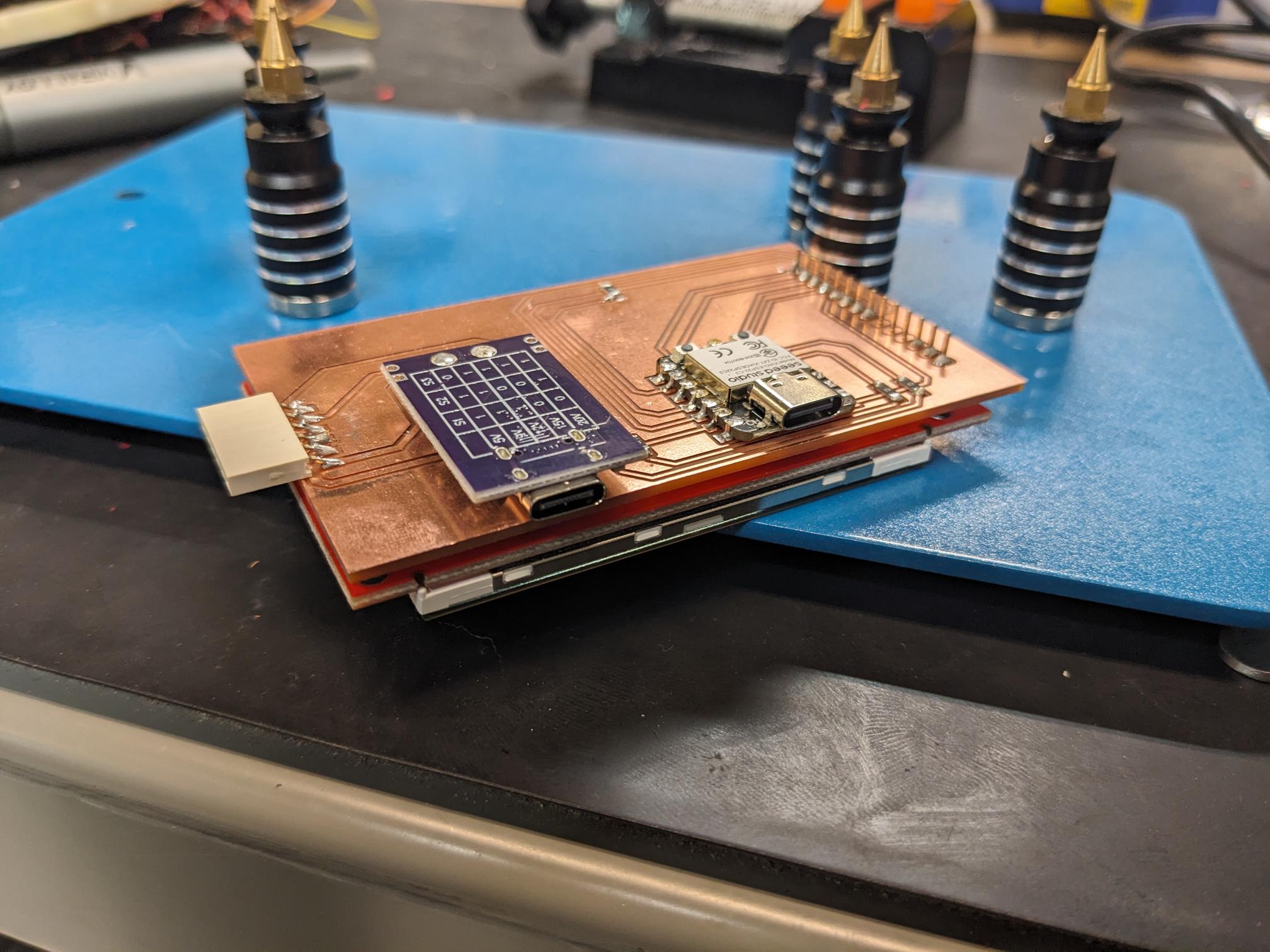
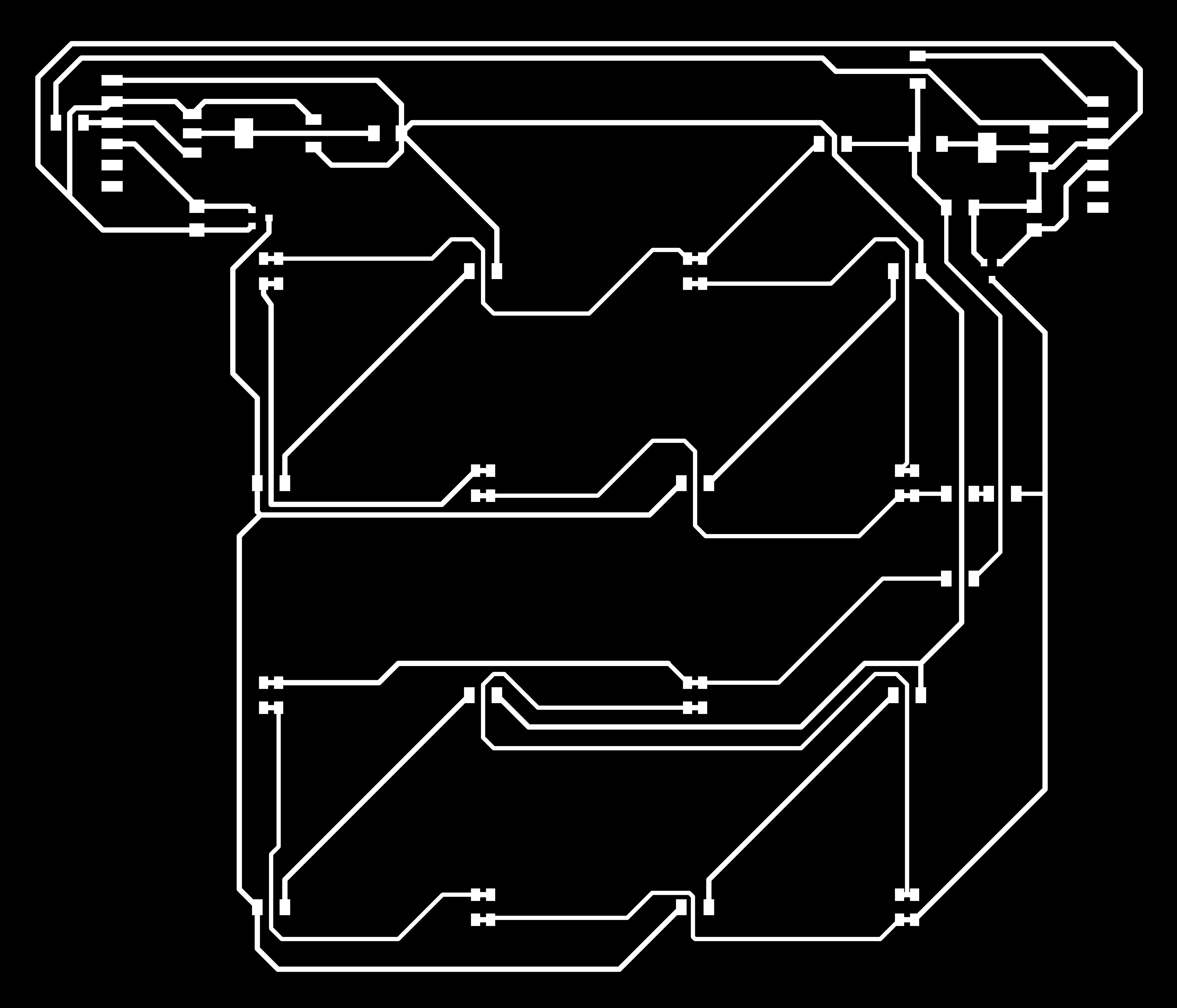
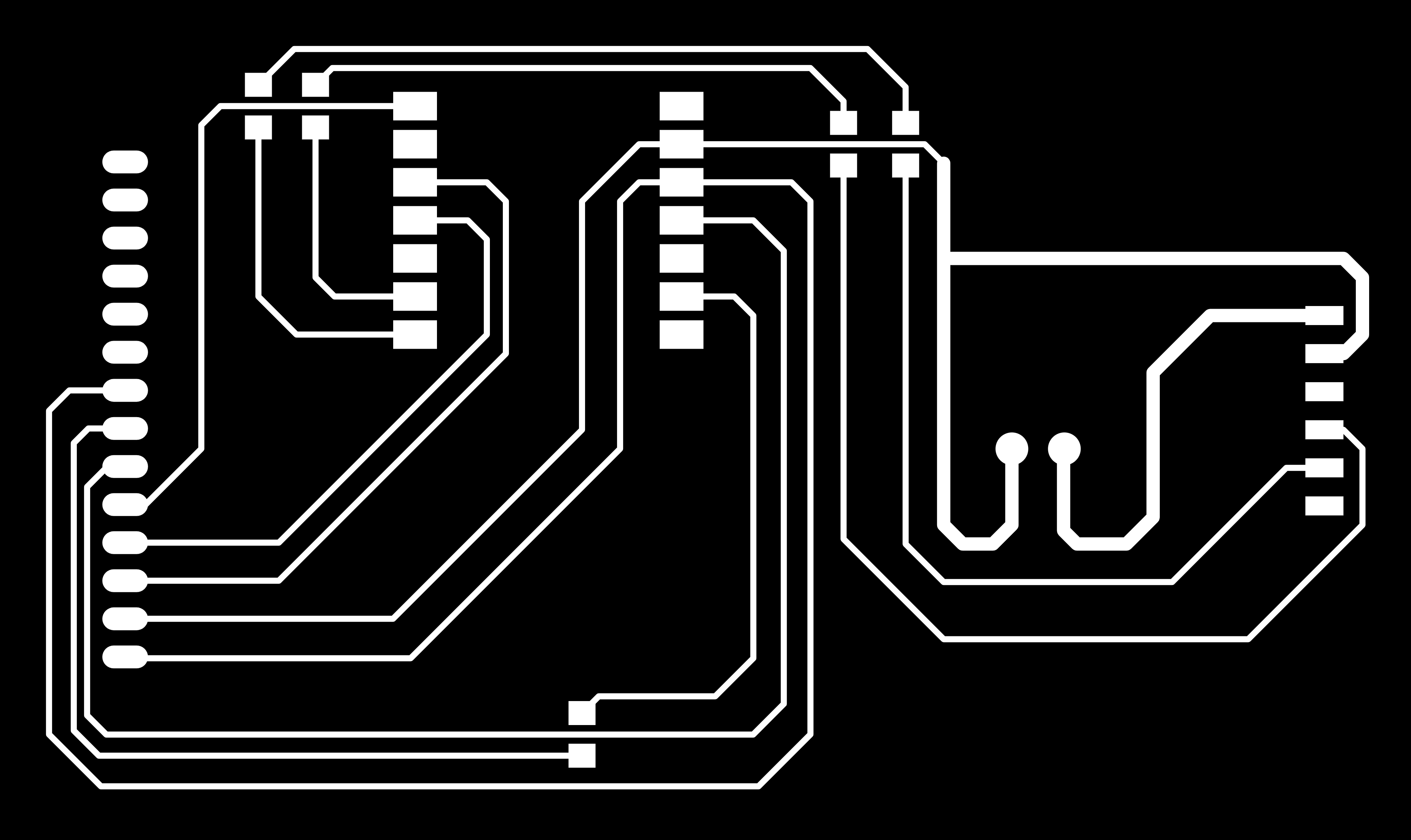
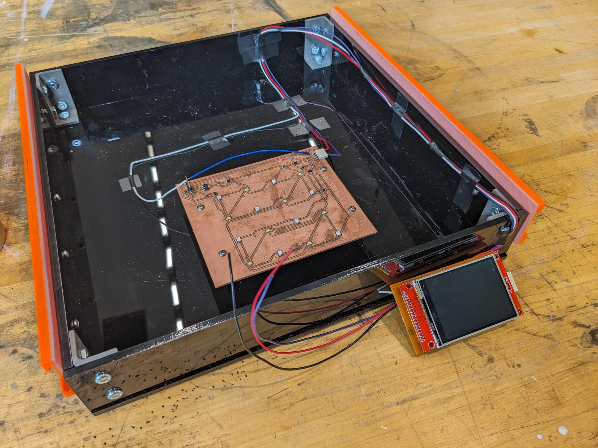
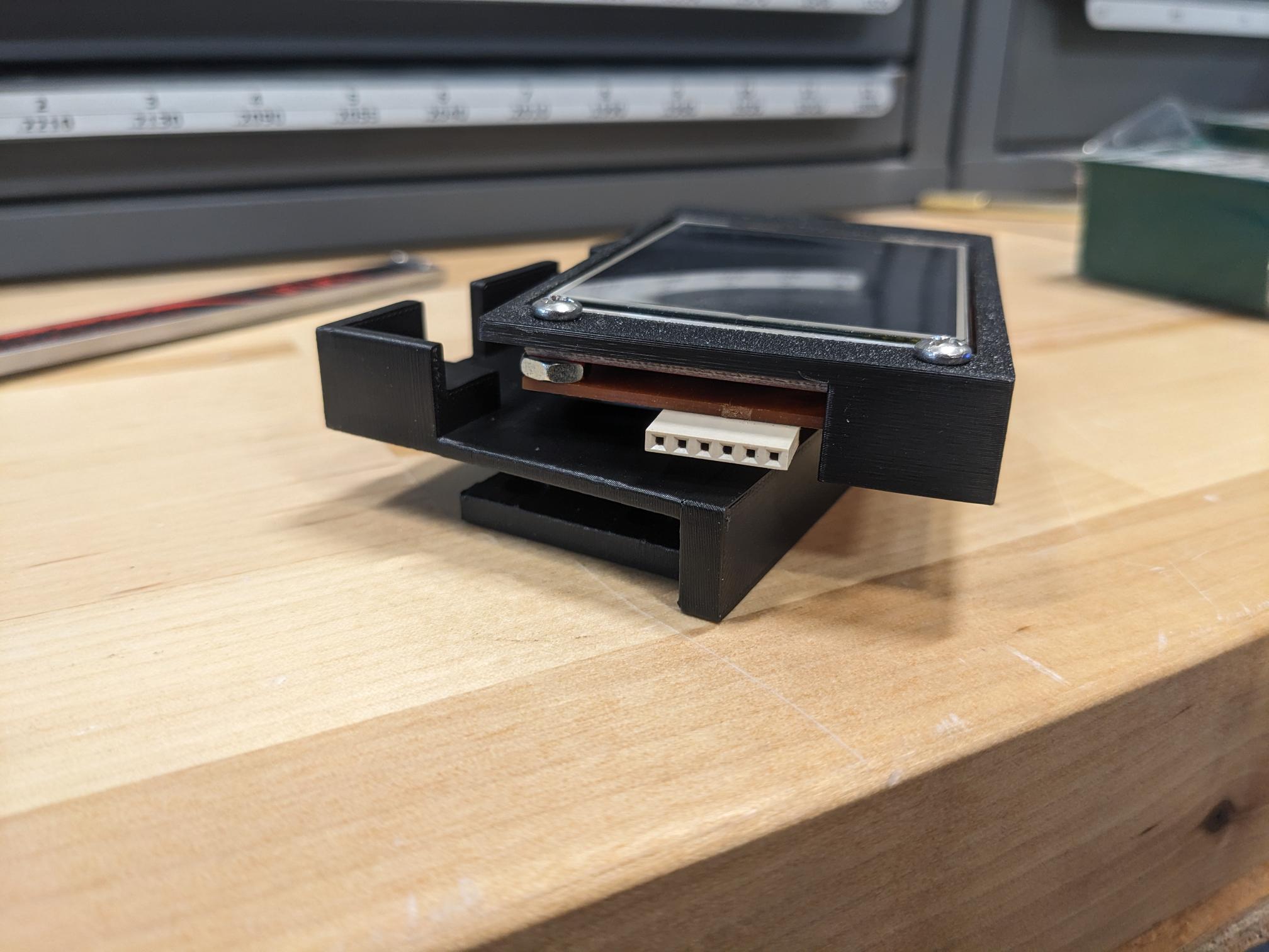
For this project there are two boards I needed to make, the first of which is my light source. This board contained two sets of LEDs, one set of which were bright white LEDs and the other is UV LEDs that I ordered off Amazon for this project specifically. I wanted the user to have the ability to operate either of the two types of LEDs depending on the available photoresist. I initially created and tested this board during Week 9 - Output Devices, so there are more details on the circuit layout, design process, and fabrication efforts there. That being said, since making the board in Week 9 there are a few adjustments that I made now that more design decisions have come into play. The first decision I made was how I am going to power the two sets of LEDs. I had found that with a 10kOhm resistor acting as a load off of the MOSFET, the white LEDs needed a supply of about 7V where the UV LEDs operated pretty well at 8-9V. There is a USB power regulator board that is kept in the class inventory where the output of the supply can be controlled by toggling three switches, and one of the settings is for 9V. This component is super useful because I designed the light source board to operate with the supply voltage going through regulators, or the voltage can be directly supplied to the LEDs and bypass the regulator. This would allow me to supply 9V to the UV LEDs while then running the 9V through my 5V regulator to supply voltage to the white LEDs. Or at least I thought. As it turns out, even swapping out the 10kOhm limiting resistor on the white LED side with lower values did not increase the brightness as I had hoped. Even with a 10Ohm resistor, I needed an input voltage of about 7V which would require a new regulator. The solution I came up with is to just use the bypass pathway I implemented to supply 9V to both the white and UV LEDs. I then increased the resistor on the white LED side to a 100kOhm to limit the current more now that the voltage was higher. Other than that the design of this board is the same as that in week 9.The second board that I needed to make was the control board that contains a screen, the USB-C power board, and the XIAO. I had done a lot of work in Weeks 12 and 13 on getting an ESP32C3 to talk with a SPI TFT screen module from the class inventory, and to implement a UI that sends/receives information. Unfortunately I was unable to get the touch working for reasons that still escape me, but the code and wiring worked really well on a breadboard level. I then started to design a PCB that would implement the same electrical connections between the TFT and the XIAO, It would also include two PWM control signals coming off the XIAO for setting the white and UV LED power levels, and it had the 9V power lines coming from the USB-C breakout board. I set the form factor to roughly match the size of the TFT with the intention on creating a case/housing that I would then 3D print in the following days.
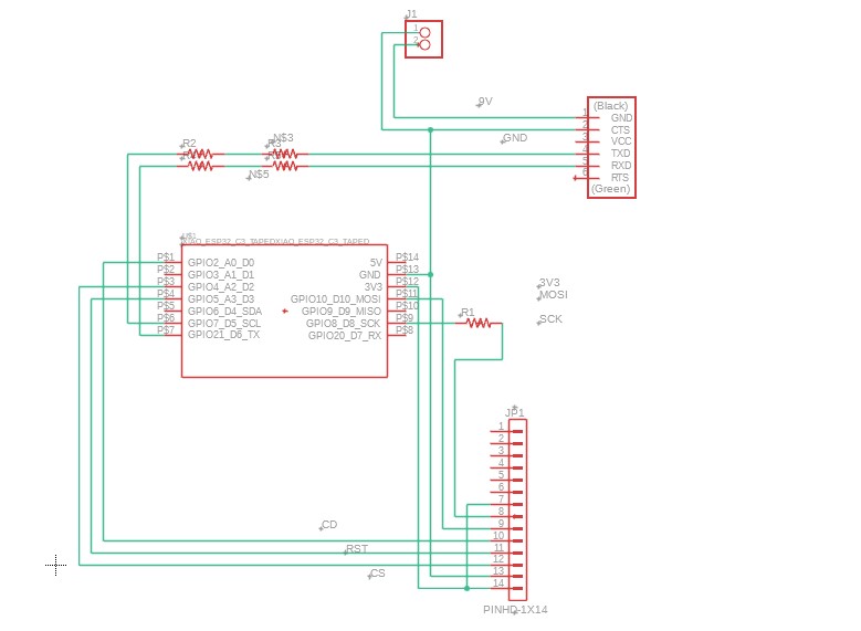
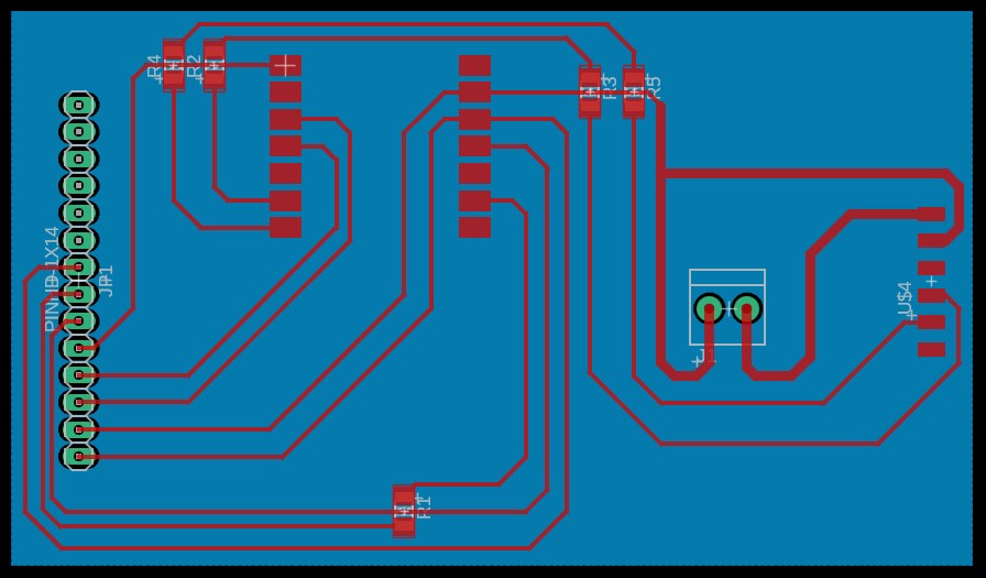
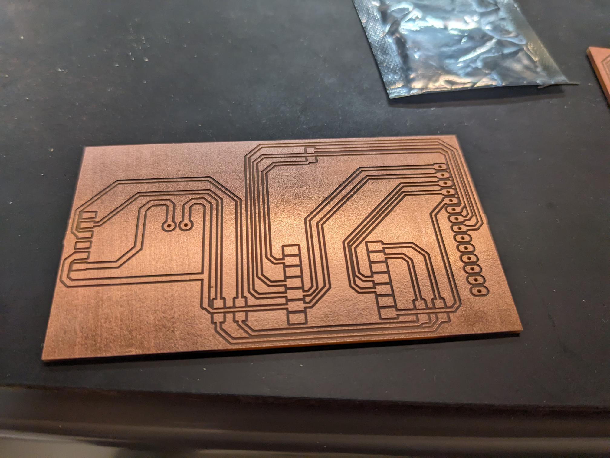
I had intentionally designed the board such that the XIAO and the USB-C breakout would be on one side of the board, and the TFT would be on the other side with through holes to allow the pins to be soldered to the traces. This worked out really nicely, although I did realize that I actually needed to flip my USB-C board because I did not label the + and - terminals of the block well. This did not end up being a problem though, and the board came out great! As usual this board was also produced with the same flow (gerb2img, mods, and Carvera milling) as all the other CNC-ed boards I have made for this class.
- Light source board footprint gerber file
- Light source board top copper gerber file
- Light source board outline png
- Light source board traces png
- Light soruce board job file for the Carvera
- Control board footprint gerber file
- Control board drill file
- Control board top copper gerber file
- Control board outline and drill png
- Control board traces png
- Control board job file for the Carvera
User Interface and Control Code
Some of the controls for this project had already been hinted at in the previous section, but when it came to writing the software needed to operatre this tool I was able to make a lot of progress as part of the weekly assignments. In Week 9, I tested the light board I made with a script that that ran a few different power levels. I modified some code that was on the class page to run a PWM loop off one of the digital pins of the XIAO with a hard coded maximum amount of cycles that the LEDs could be on for. This effectively sets the 100% power level the user can choose, and all other power levels are then the fraction of the max cycles possible. With a digital pin each to control the white and UV LEDs, I experimentally determined what the max cycles would be based on brightness and power draw whcih was 1000 out of 5000 cycles high.In Week 12, I used the assignment to work on communication protocols to get SPI up and running for talking with the TFT screen module. Again, the hope was to also include touch which I was unable to do, but I at least figured out how to write text and shapes to the screen. I made a rudimentary display that would eventually just act as an indicator for the user to know what parameters they are exposing with and to let them know an exposure was running.
And lastly, I used Week 13 to get my laptop to send and receive data from the XIAO with the use of a simple user interface. The site is a locally run HTML page that connects to the XIAO through a serial port. Both the website and the Arduino code send and read bytes back and forth to communicate the parameters set by the user. With all the work done during these individual weeks, I then needed to get all of it to come together. The final code made use of the PWM loops developed in Week 9, which are set and controlled by the websocket code created in Week 13, and the data for this is output on the TFT screen based off code developed in Week 12. For the most part it all integrated together nicely, but I did need to tune the PWM cycles a bit. My best guess is that because the main code runs the PWMs in a while loop rather than running the cycles in the loop() function, the execution time was slowed down since the while condition needed to be checked constantly. I just needed to bump the max on cycles to 3000 rather than 1000, and everything seemed to work well from there.
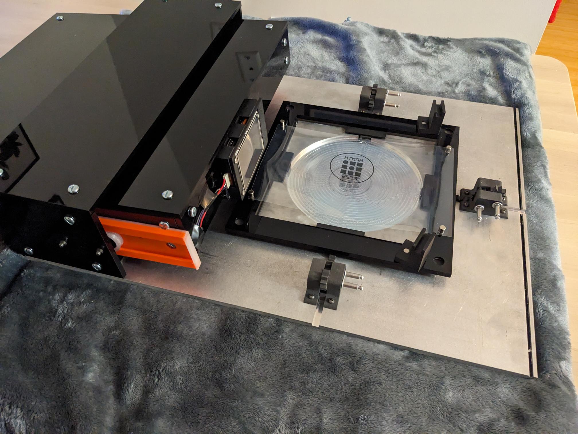
Final Assembly
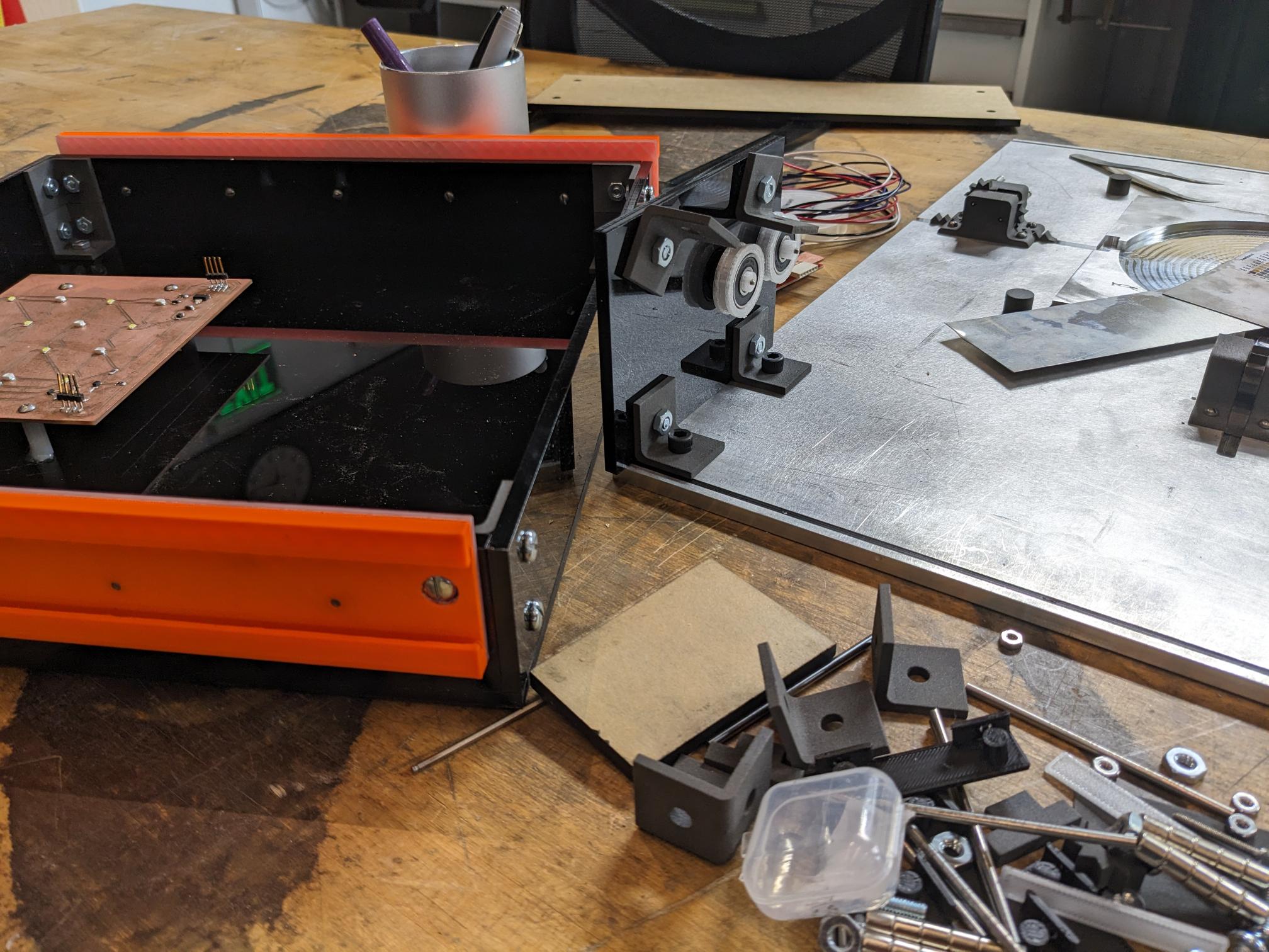
When assembling my final project, I started from the base plate and went upwards. I started by adding in the mask frame stand offs and screwing in the first layer of parts. This included the brackets used for the acrylic sidewalls, and the nylon gear assembly parts. I did need to sand the standoffs and some of the gear assemblies down a bit just to make sure that they fit well, but this was a pretty low lift. I wasn't entirely sure what rod-like material I would use for the gears, but I found an 1/8in pin set at the hobby shop that was not what I had envisioned but ended up working really well for my project to hold the gears in place.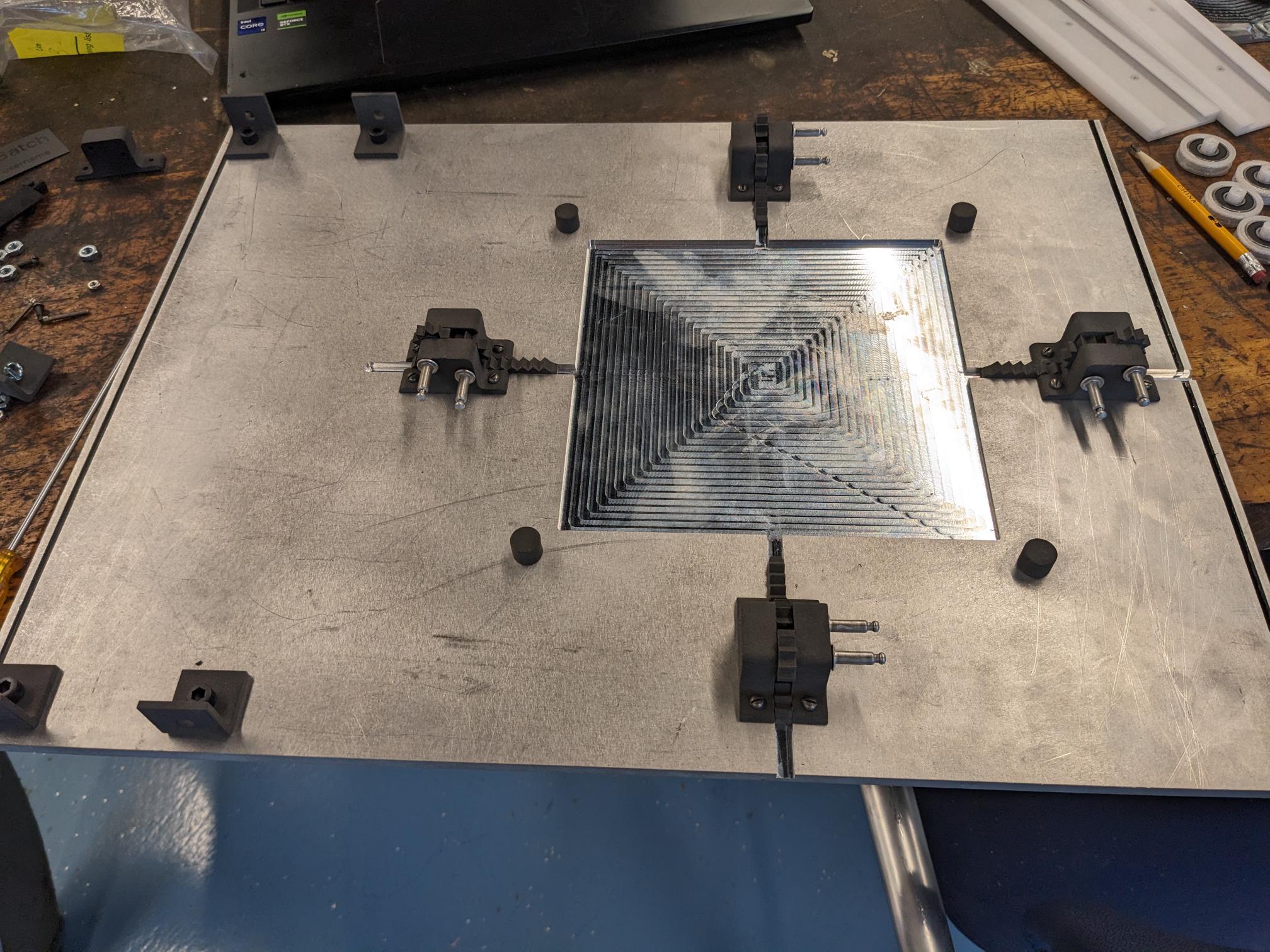
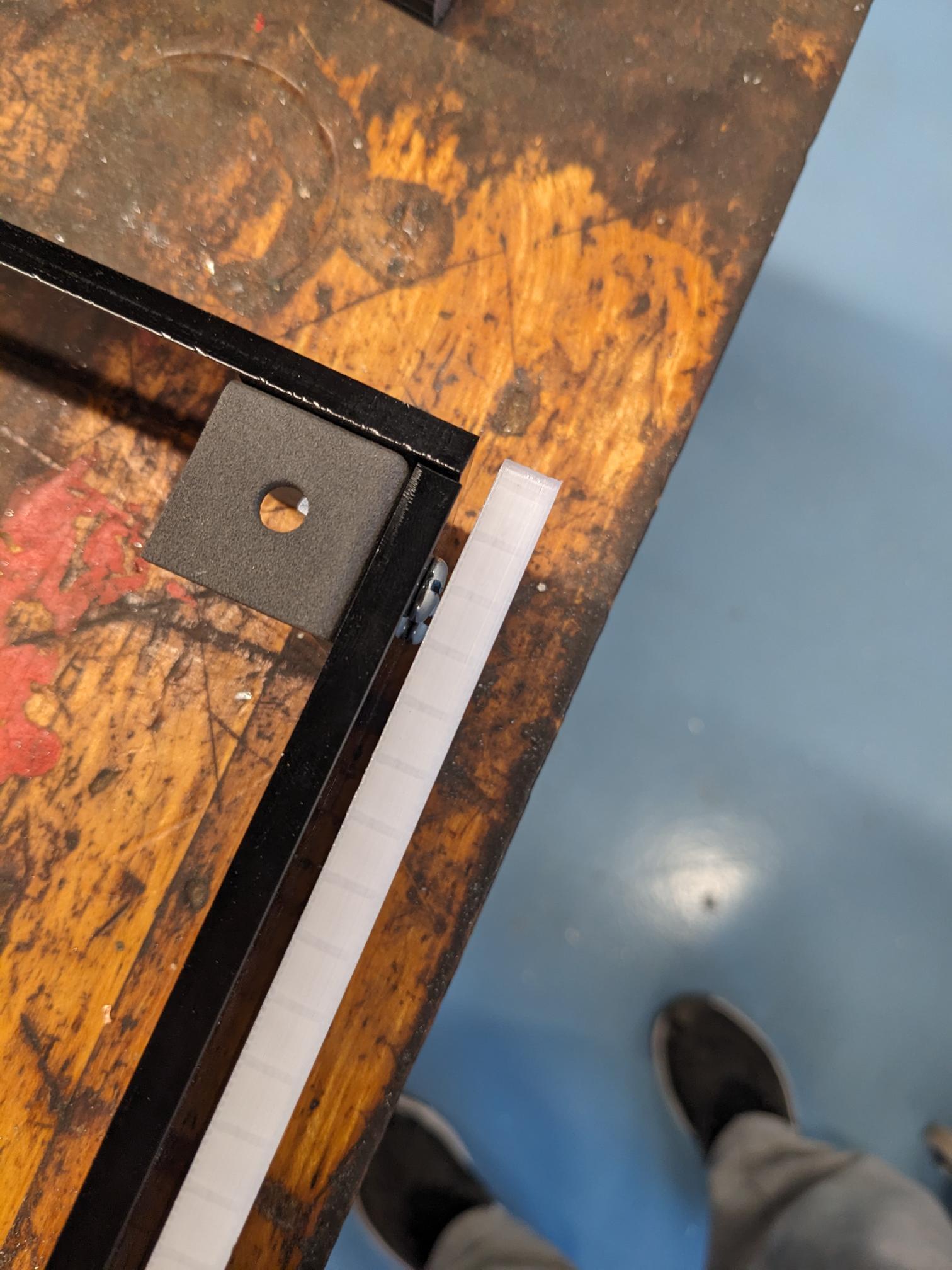
Next up was the light box itself, which mostly consisted of the acrylic parts. These were easy to assemble, but when I went to fit the rails on the sides I encountered my first problem. I did not account for the screw heads coming off of the light box, which caused my printed part to bend and fall out of tolerance for how my project was meant to fit together. I gave an attempt at drilling a hole in the part to accommodate the screw, but ultimately found it was best to re-design the part and to print it again. Sadly, I somehow did not get the diameter of the screw head right or maybe entered the radius as what was meant to be the diameter, because when I tried to install the new parts the dimensions were slightly too small. I also realized a bit too late after the fact that my rails are not designed to be symmetrical. So when I added the new features one of the rails fits as intended while the other rail still fits but is offset by about 1/4 to 1/2 an inch. Regardless of the positioning, I still had enough travel to fully expose my chuck area so I decided to move ahead for sake of getting the project done on time.
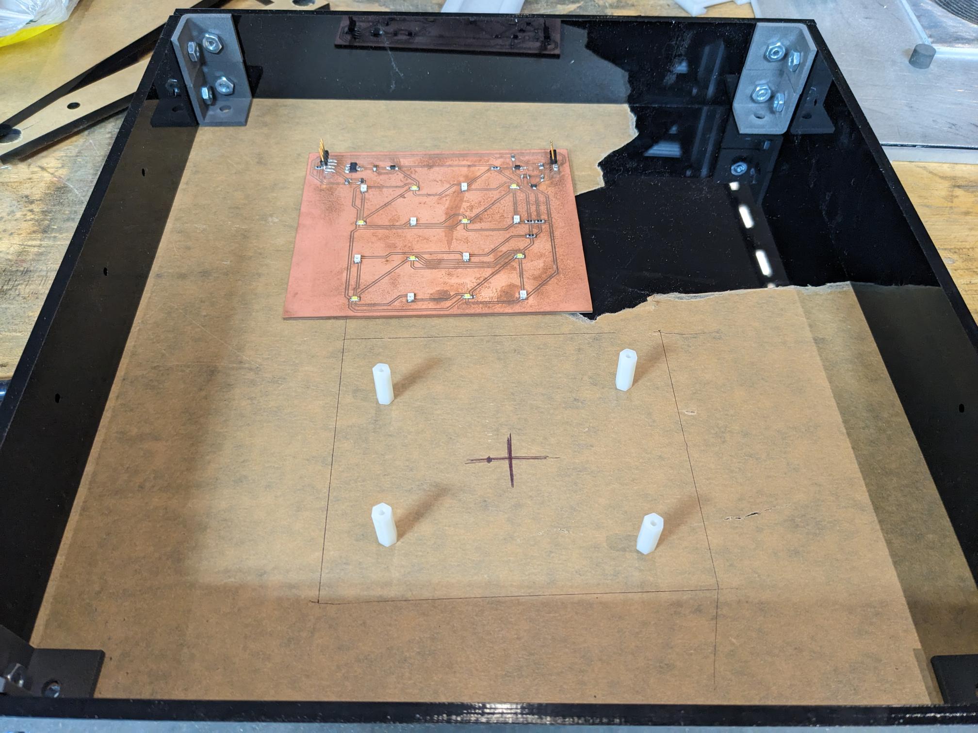
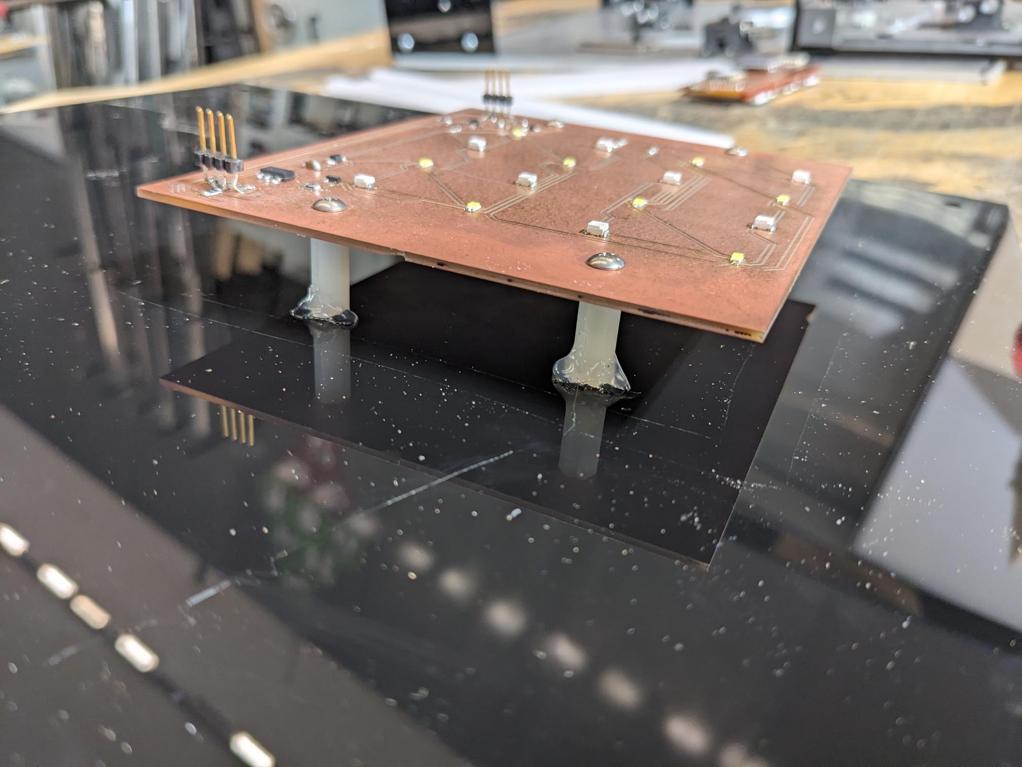
While the new rails were printing, I figured out the placement and mounting mechanism for my light board. I mapped out where the footprint should go and used nylon standoffs from the CBA community parts shelves to position it a little bit off the acrylic. The nylon standoffs accepted 4-40 screws, so I drilled holes in the PCB where no traces were and screwed in the standoffs. I then aligned my board to the footprint I had mapped out and glued down the standoffs with a hot glue gun.
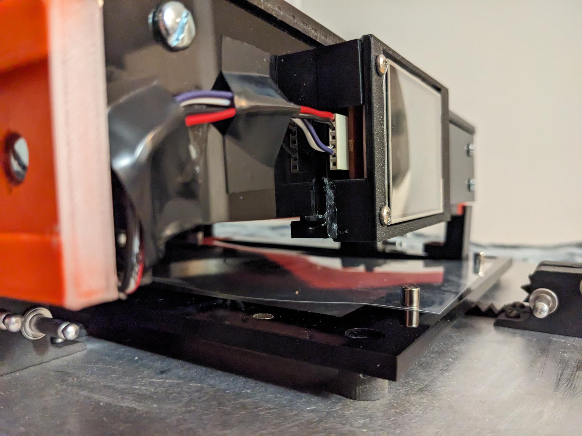
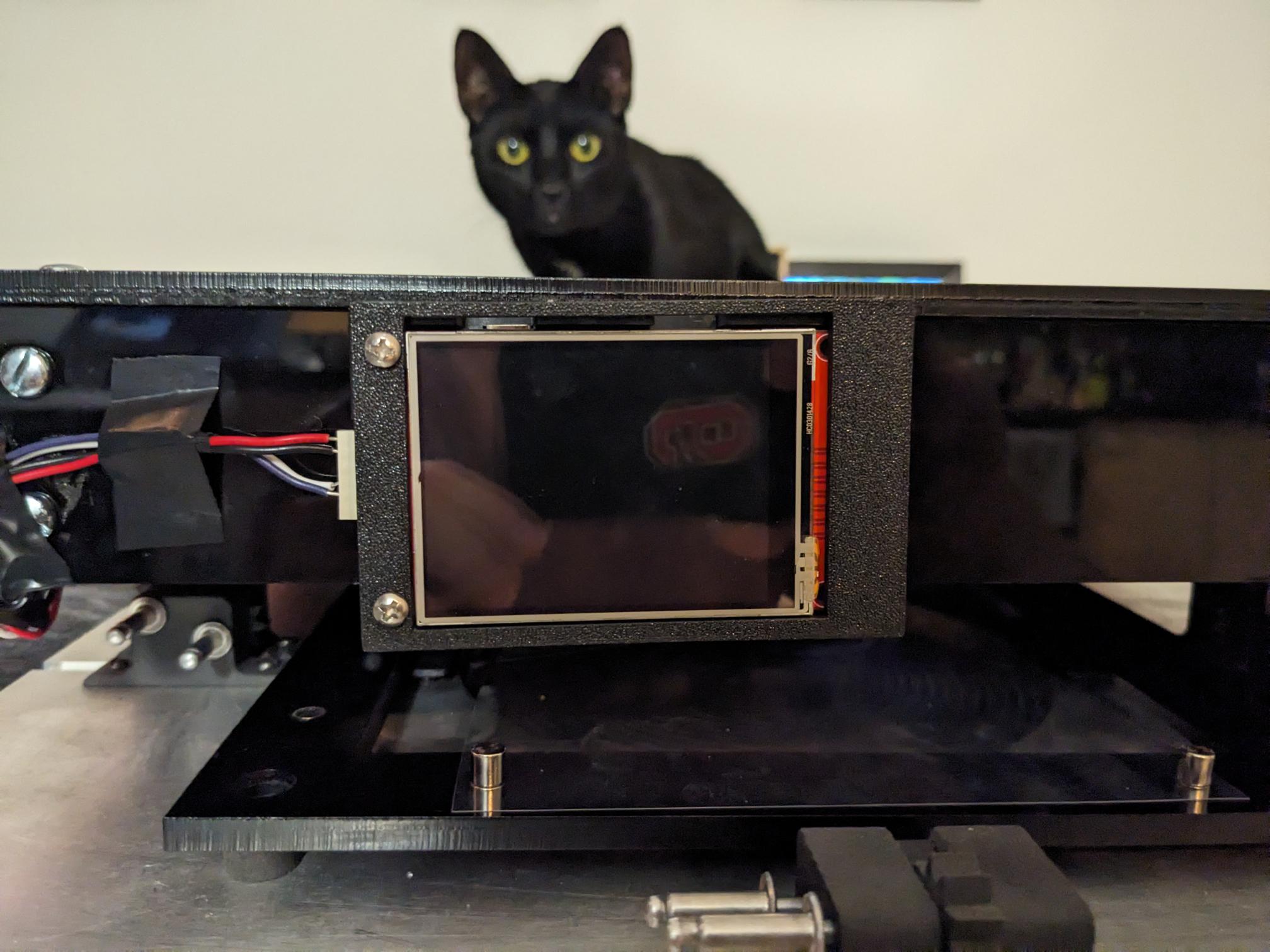
I initially planned on having the TFT screen mounted to the base plate, so I started to route and secure wires to the back of the light box so that it would be able to reach the TFT from the fully pulled out position. Instead, I realized that I could print a housing for the TFT and have the screen mounted to the light box itself, that way there would be no issues with moving wires as the light box and screen would now be moving as one. I made sure that I had enough wire length which I did, so I tentatively routed the wires to the front of the board where they would then get connected to the screen once it was ready. At this point in time the rails had finished printing so they are also attached to the light box in the following images.
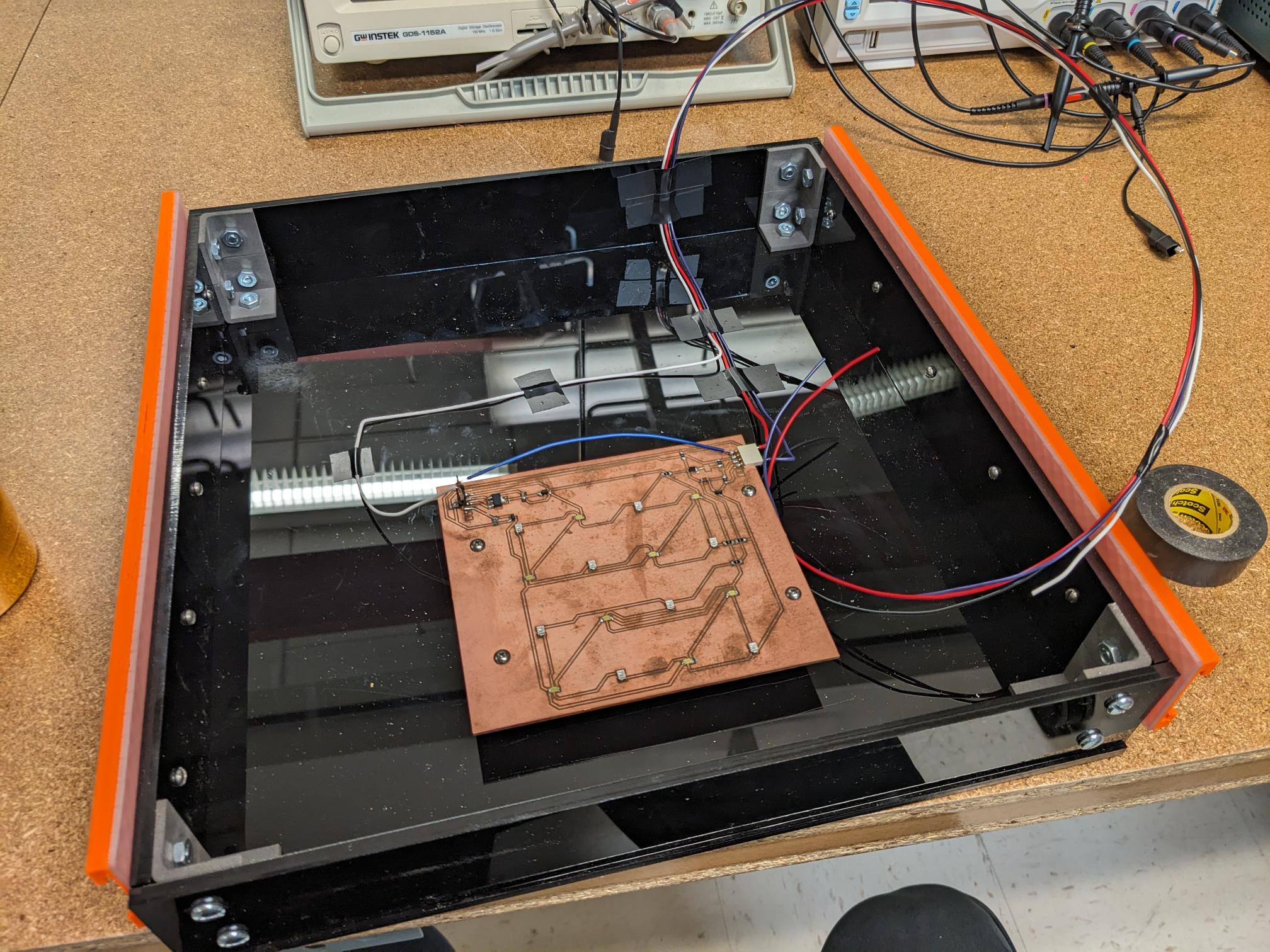
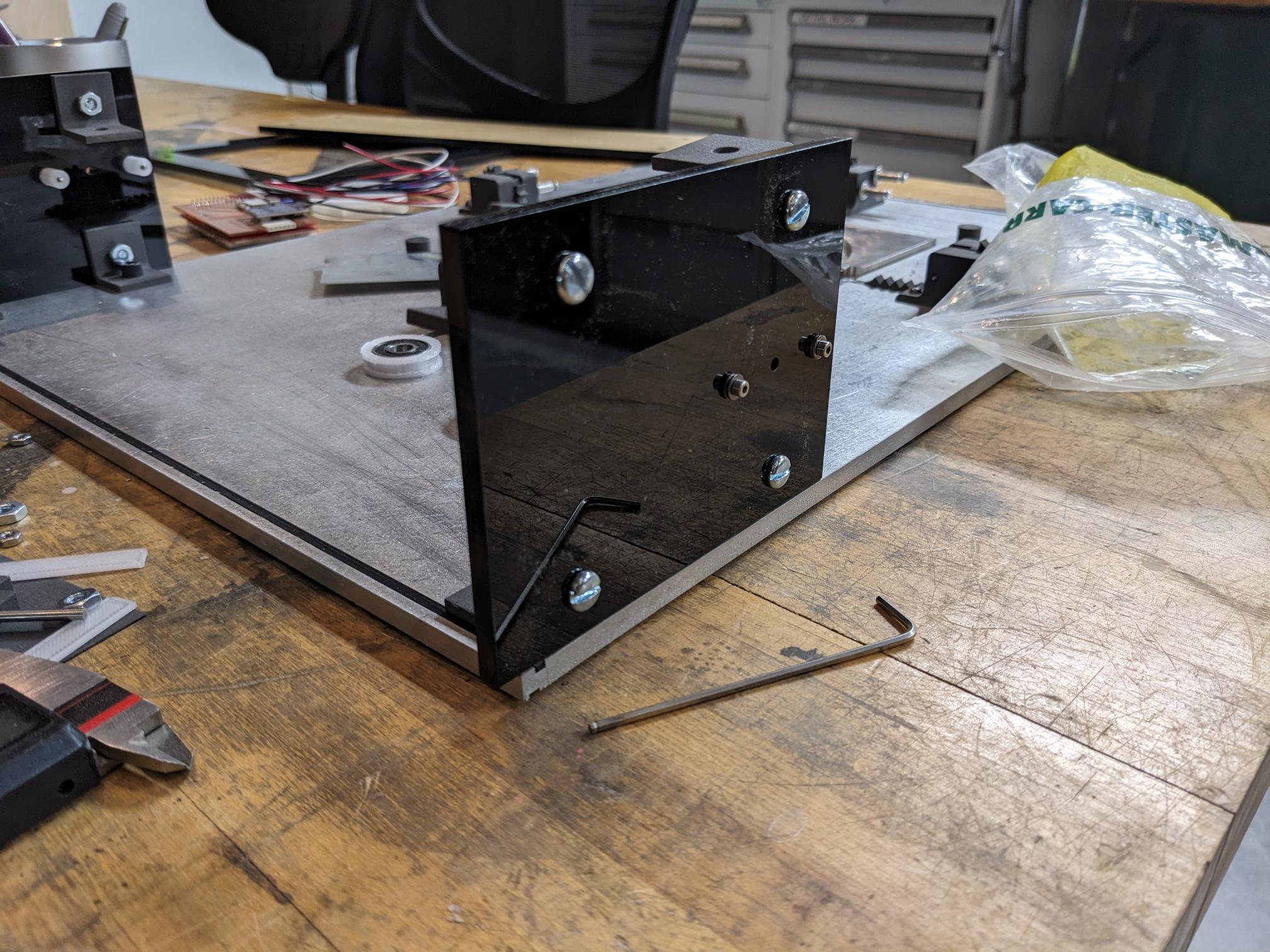
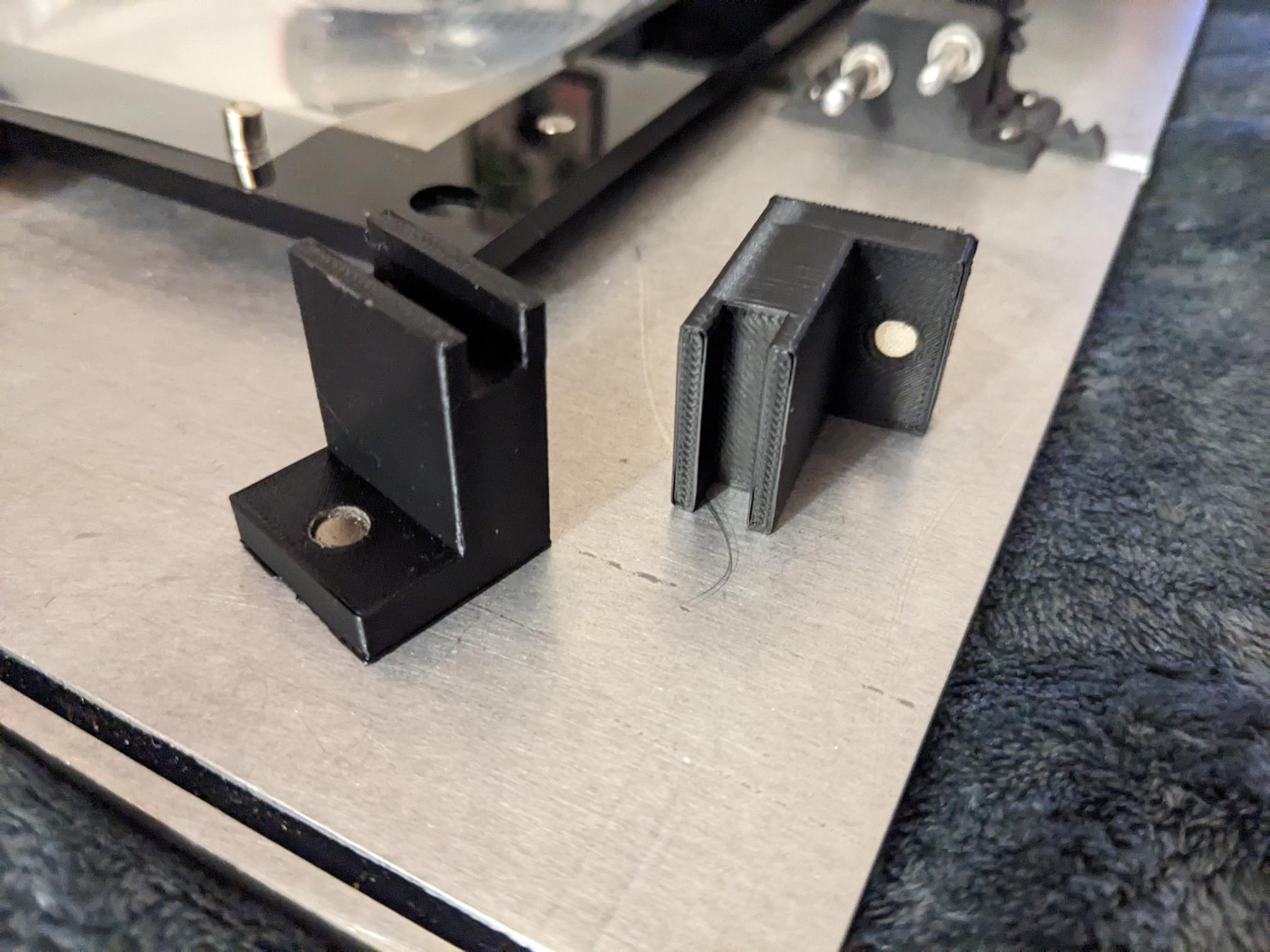
At this point I put the sidewalls (and top acrylic) on the main base plate and screwed in the ball bearing fixtures. I then slid the rails on which took a bit of finagling at first because I had not cleared away all of the 3D printed support material. I was able to see that my spacing was correct and everything was at the proper dimensions, but I went back to clear the additional material before re-positioning my rails. I then glued the end caps on to make sure that the light box wouldn't slide too far and come off the ball bearings.
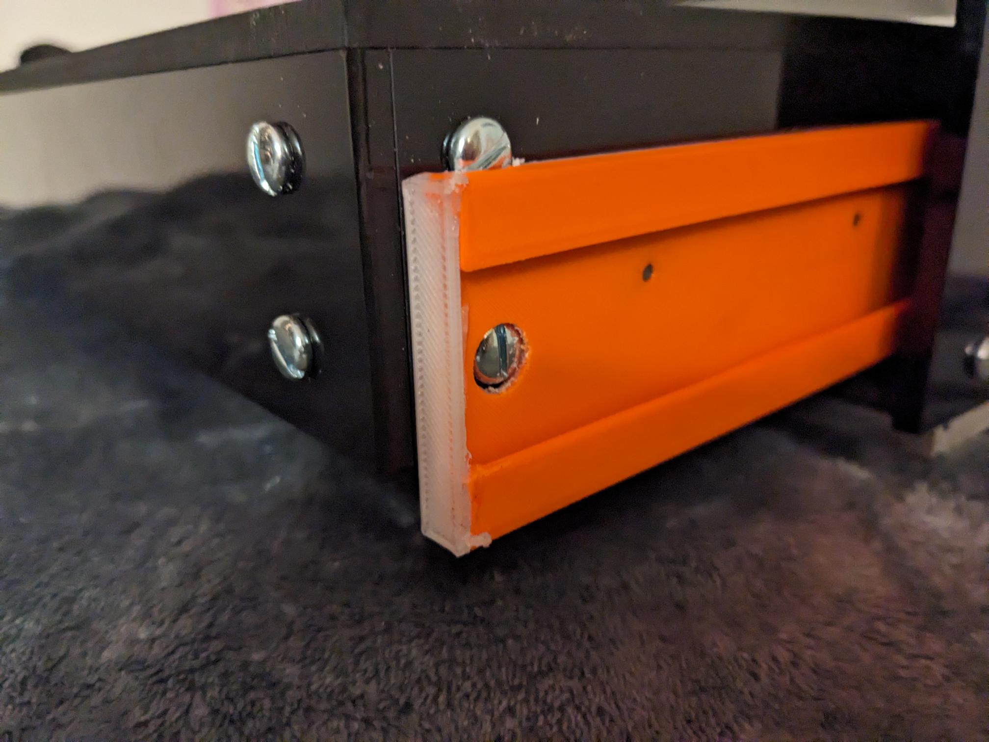
While testing the sliding mechanism I encountered the second issue that I did not anticipate. The problem was that my material stackup and dimension tolerances did not result in a completely rigid structure to support the sliding light box. As such, when fully pulled out over the substrate area it would sag downwards. Now this isn't really much of a problem because worst case I could just have the front rest on the mask frame and that would be good enough, but I figured I could come up with a cleaner solution. The method I devised was to add two more magnet holes to the new mask frame design (since I had not made it at this point) which would accommodate 3D printed standoffs that fit the thickness of my acrylic. These were really easy to design and print, and they fit their purpose very well. Not only are they the proper height for the light box to rest on, but it also helps give the user a consistent spot for the light box to be extended out to. These standoffs were printed at the same time as my TFT case, which meant I could finish my assembly. I did use more hot glue to secure my case pieces because a few spots were a bit flimsy, and I used more hot glue when mounting my case because I did not have the screw holes in the acrylic which would be great to include on a future iteration.
Testing!
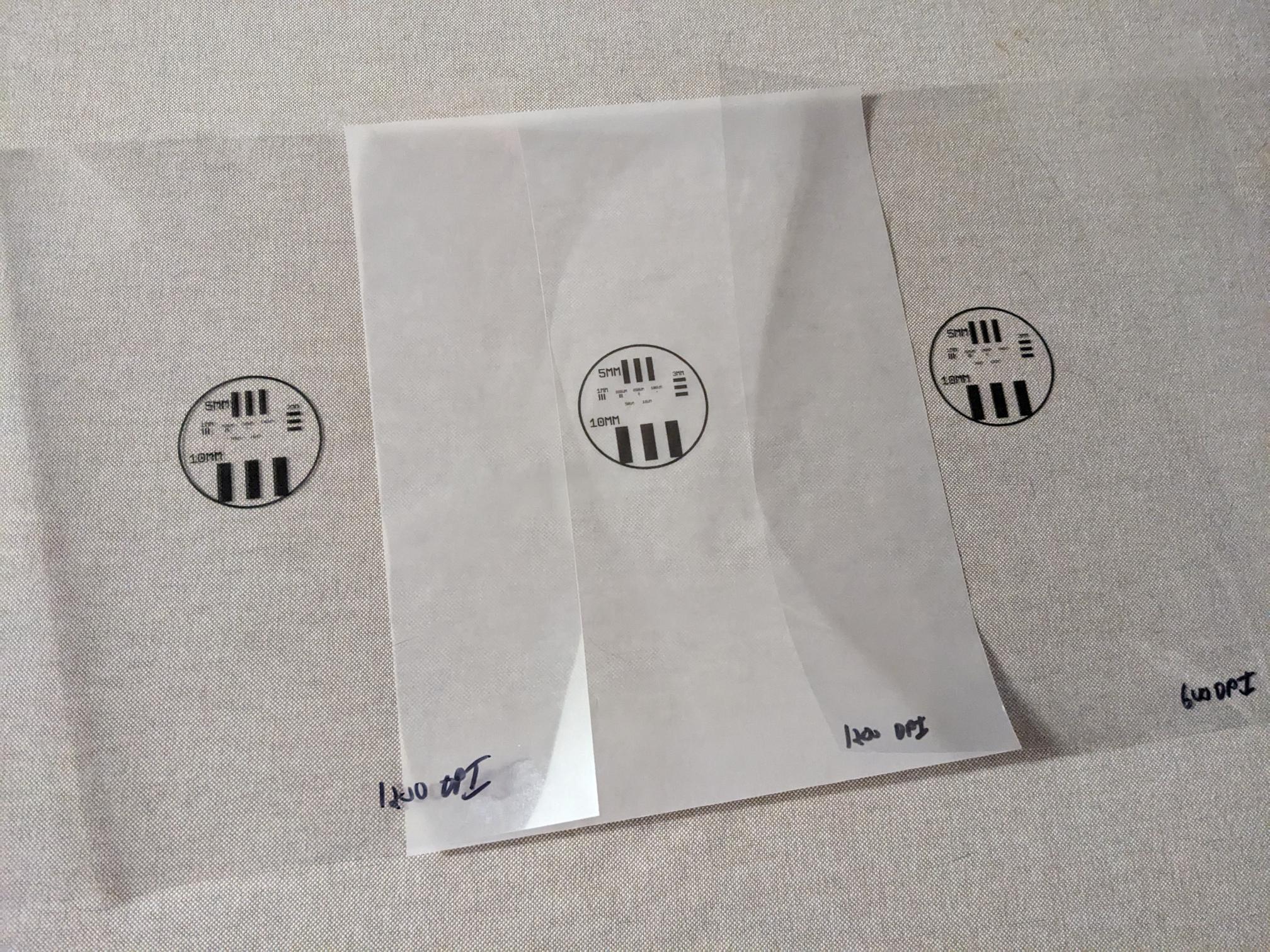
In order to test my device, I needed material that I could make shadow masks with. From my experience working in semiconductors, I knew of a material called Mylar which is often used for this type of crude mask work. Sadly, it is very expensive and is not offered in large enough sheets that I could run through a printer. Instead, I ended up just buying a cheap set of transparent 8.5x11 sheets off Amazon. I did see some forum notes online that people suggested using vellum paper, which I was skeptical of but I still ordered 8.5x11 vellum paper off Amazon as well because it was ~$10. When they arrived, I started by printing multiple test masks of a layout I made in a common mask making software called KLaout. My design contained a bunch of different sized lines in a 2in footprint so I could see what the resolution of my tool would be. I used two different print settings, 600 dpi (dots per inch) and 1200 dip, and I printed the design on both vellum paper and the transparent sheets.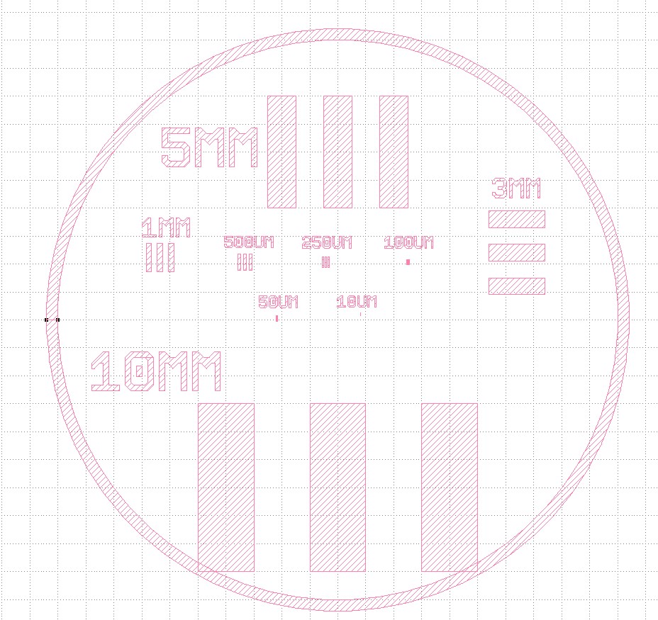
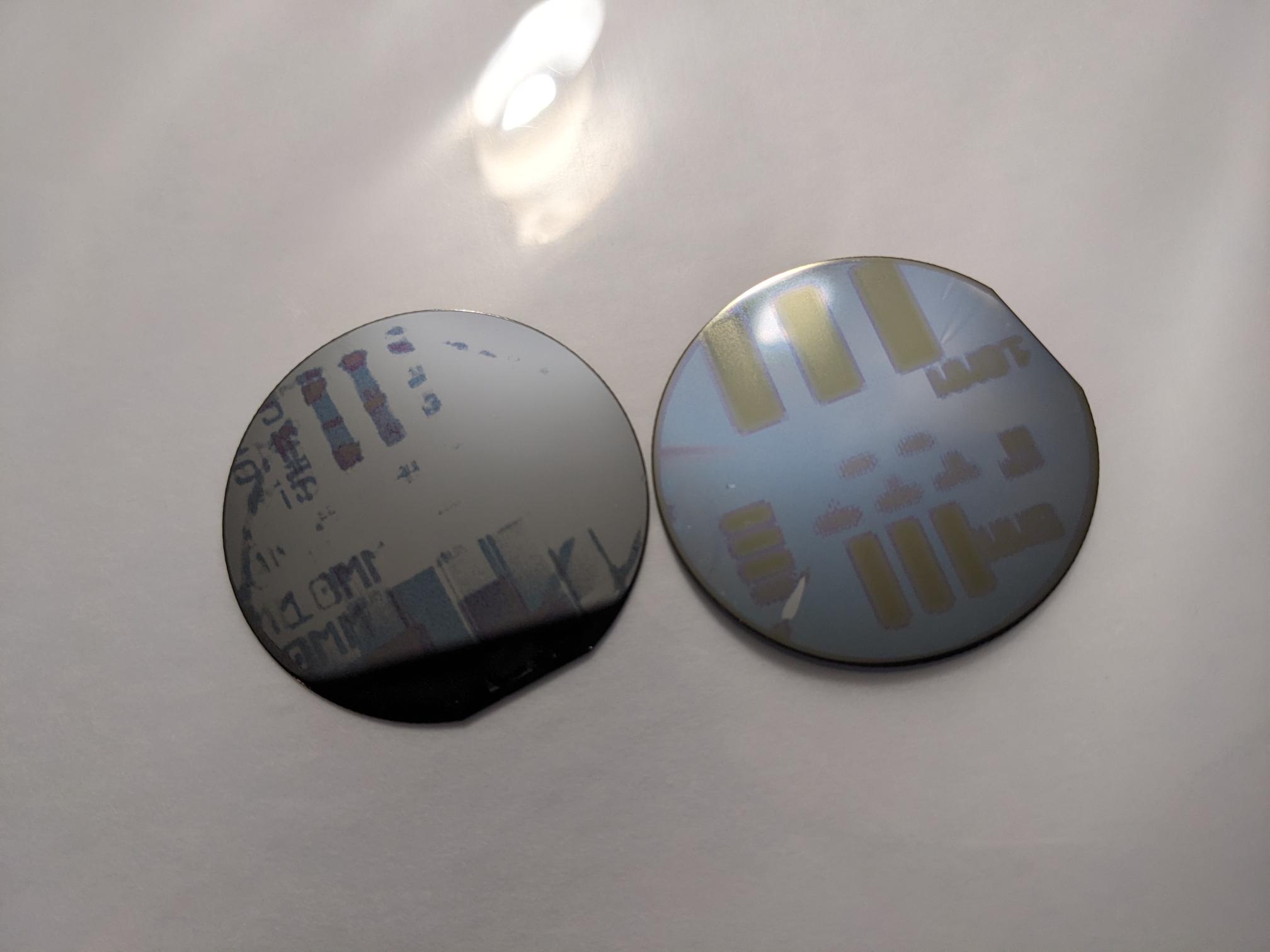
There are a lot of parameters that can be used for lithography, so I simplified my resist process by using the same resist and always spinning it up at 3000rpm. I used the same post apply bake of 110 Celcius for 60 seconds for each run, and experimentally found that a post exposure bake of 110C for 60s was also beneficial. The development process used a .26 normal TMAH developer, but I developed my patterns until they were mostly or completely resolved rather than developing for a set period of time. The variables I then had to play with was how I used the mask and what my exposure power was (I chose to expose for 60s on each run). The first wafer I tried surprisingly did create a pattern, just not a good one. I was honesty a little worried that I wouldn't be able to get anything to print whatsoever, so this was a really good proof of life for my tool! Looking at the pattern I found that each individual LED created a slightly different version of the pattern on the wafer, meaning I would not be able to do projection lithography with how my LEDs were set up. I then tried an exposure with my wafer in contact with the film which worked better, but even the thickness of the transparent sheet caused some blurring around the edges of the 10mm features. At this point I also tried exposing with the vellum paper, but I was unable to even clear the resist so I decided I was not going to both much with it going forward. The most successful test came from flipping my transparent mask around so the printed surface was face down on the wafer, with is the rightmost wafer in the images below. It looks like the pattern transferred very well, and upon inspecting both the mask and the wafer I found that I was actually being held back by the quality of my printer. I was using an old ink jet printer, which means that the ink gets sprayed onto the surface of my sheet but it does not absorb into the material the same way it would with normal paper. As such, looking at one of my masks closely showed there are very small gaps in the printed surface which is allowing some light through and is messing with the quality of my print.
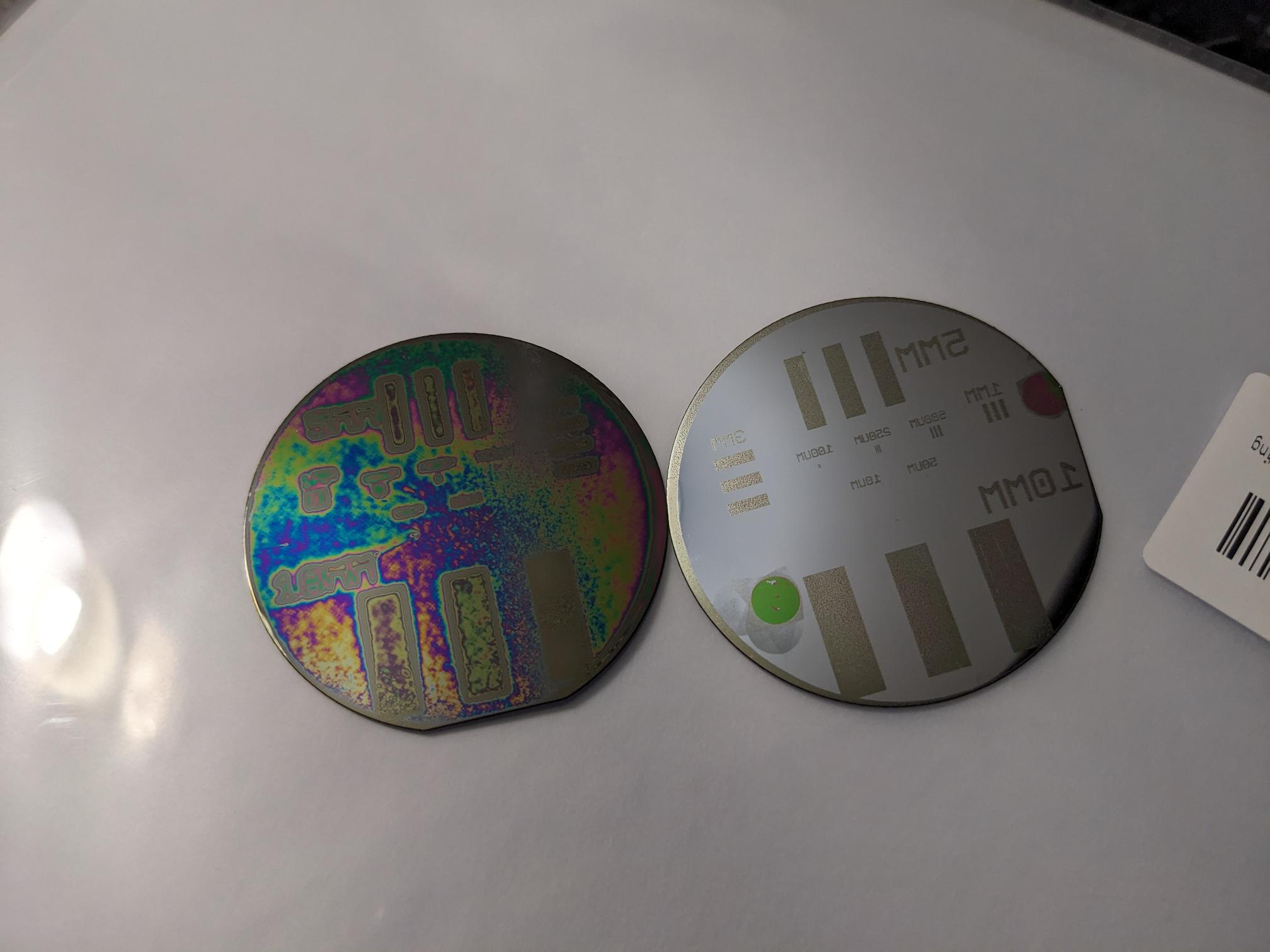
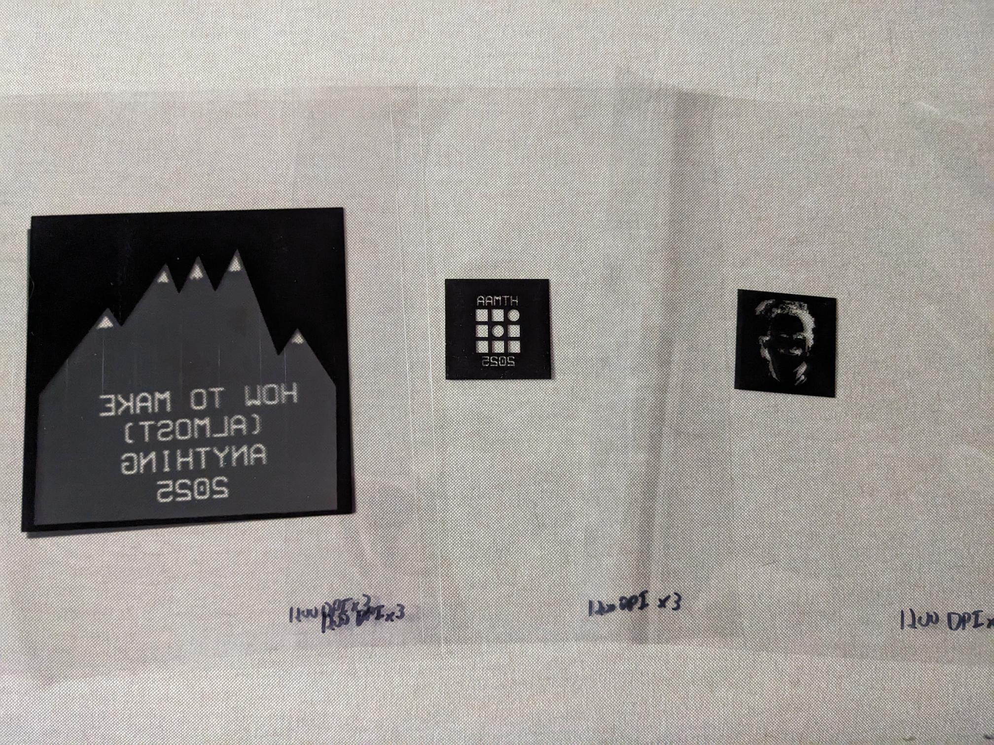
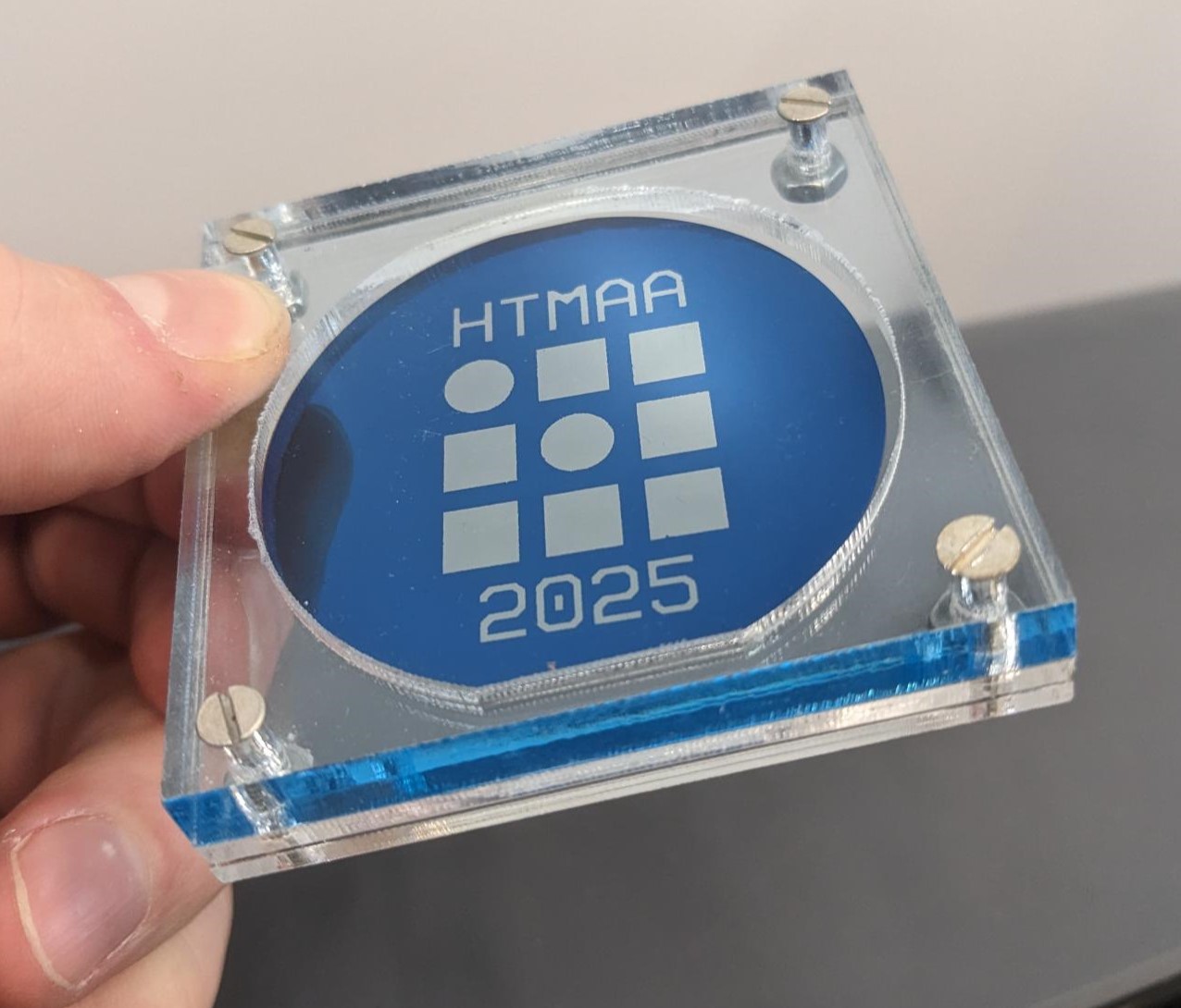
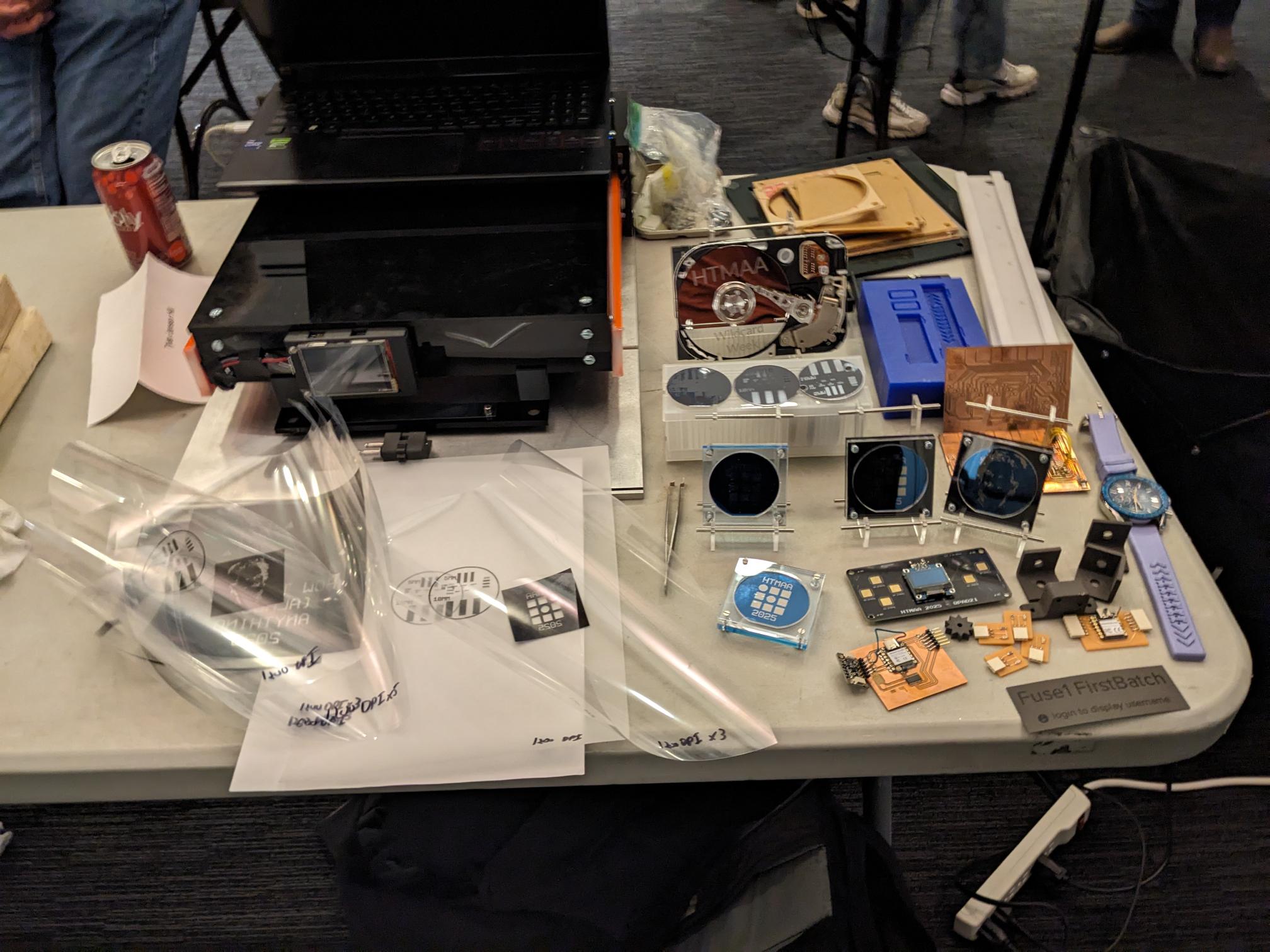
I could not find a better printer in the short time I had left to test, but I did run my new masks through my printer a number to times to try and minimize any gaps between the pixels. I did need to make sure that I was printing my masks reversed though in order to account for having the print side down however, but that was not hard to do. I printed a mask with the CBA logo and "HTMAA 2025", a two-tone image of Neil, and two patterns that could be aligned to one another to make mountains with a snow peak at the top. I did not actually make the mountain wafer because that would require a 6in wafer and additional processing I did not have access to, but the individual wafers came out great! Sadly I didn't take a direct picture of Neil's wafer which came out just okay, but it is in the overall picture of my table setup during our final presentations. I did put the wafers in acrylic cases cut on the XTool P2 to protect them from breaking and from dust.
Outlook and Future Work
Part of me is still somewhat surprised that I was able to make this tool work, and I'm specifically surprised that I was able to hit the resolution of my printer which is just super cool. With that in mind however, this project is still not perfect and there is a lot of additional tooling needed to make a single photolithography step doable. I already pointed out that the holes on my rails are not lined up properly, and I needed to 3D print supports for my light box because it sagged. These are smaller tasks that I would like to fix but are not my highest priority. The first goal in improving this design would be to re-do the mask alignment process to turn my tool into essentially a contact-aligner. I plan on designing both electronics and hardware to allow the user to place a wafer and a mask in a fixture, and the fixture would then automatically bring the wafer into contact with the mask giving the best resolution for pattern transfer. This could also be accompanied by a redesign of the LED board because at first I was not sure what my current limitations would be through USB-C. Now I know that I am able to supply enough current for each LED to be placed in parallel, but I also may reduce the design to single LEDs to minimize interference of point sources coming from different locations.The overall goal that I was aiming for was to be able to pattern wafers with cool and interesting pictures without the need for costly fab equipment or resources. Following improving my exposure tool, the next logical step would be to make a spin coater which I don't think would be very challenging. I would then need to figure out if I want to try and do a deposition system of some kind or focus on etches of pre-prepared wafers, but that will be a little ways away. What is very interesting for the near-to-mid term though, is that Professor Gershenfeld expressed interest in me continuing the development of these low-cost crude fabrication tools. He expressed a great vision for this project where these tools could be used for educational purposes, to get students/kids interested in semiconductors and/or semiconductor processing. I will need to look into possible transistor architectures that can be reliably created on this level, but it sounds like a really fun pathway to pursue. Regardless, I do plan on continuing development over the next months/years and I hope to be a part of the HTMAA in the Fall of 2026 whether that is in an official capacity or as a general resource. But given everything we have learned so far and all that is still left to do, I guess the real class does indeed start now!