Week 8 - Input Devices
This week we talked about a number of different sensors/useful instruments we could potentially use with our project. These included positional devices like accelerometers and GPS units, light sensing devices, temperature sensors, and many more.
Assignments:- As a group probe an input device's analog levels and digital levels
- Add a sensor to a microcontroller board we designed and read it
Probe an Input Device
Since I planned on using distributed phototransistors for my weekly assignment, I was already making what are effectively breakout boards for the phototransistor. This was perfect for the group work as we then just had to set up the power supply and oscilloscope and we were good to test the device. Details on the measurement are on the class page here.
Add a Sensor to a Microcontroller Board and Measure Something
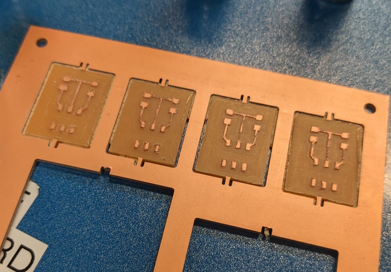
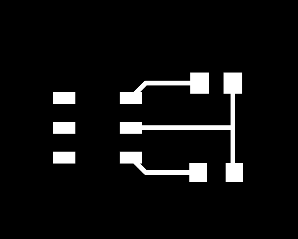
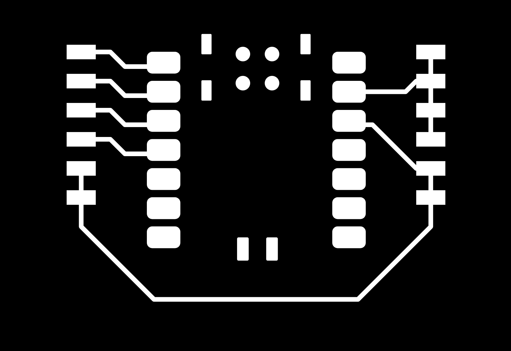
I have somewhat learned my lesson with the surface mount microcontrollers and the difficulty in programming them, so this week I really wanted to make sure I designed something that used the XIAO for simplicity. I also wanted to use phototransistors because there may be potential applications to use them in my final project as I am making an exposure tool. The idea I came up with was to do a sort of distributed light sensor setup, which could theoretically be expanded to help me measure the exposure dose of my project at a further point. There will be a central XIAO board that I will connect to and program, with a number (in this case 4) of separate phototransistor boards that can be arranged as needed and connected with wires. The schematics are very simple as I just need to provide each phototransistor with power, ground, and a single analog read pin. The schematics have dummy components in them so that I can have the pin spacing needed for the horizontal female connectors I planned on using. I know I could have just drawn the pads that I needed and measured the spacing, but I found this to be easier. Also, these boards are both one sided but I chose to use the GND plane as the footprint image when milling out my board. Both boards are below with the XIAO board first followed by the phototransistor board.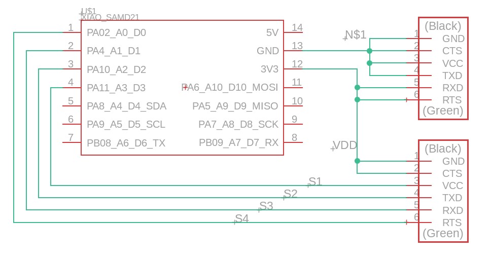
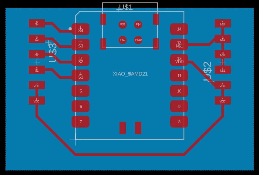

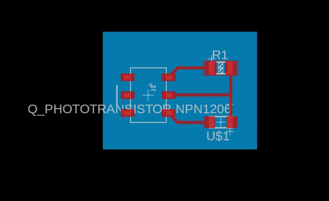
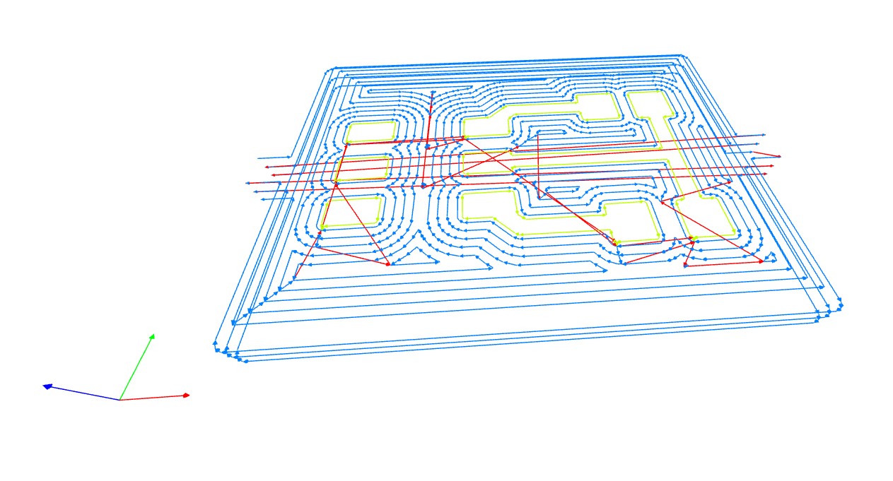
I then used the gerb2img and mods as we had done previously to set up the cut job for the Carvera. The only difference this time was that I chose to use the Carvera flow that cuts out all of the copper and just left the traces/pads behind because I wanted to see how the boards turn out. Since these boards were so small I was okay with the time add. No one was waiting for the Carvera while I was on it, so I did 4x phototransistor boards at about 9min each and the XIAO board at maybe 11-12min. In my opinion, this cut style is completely worth it as the PCBs look much cleaner than the previous ones I had milled.
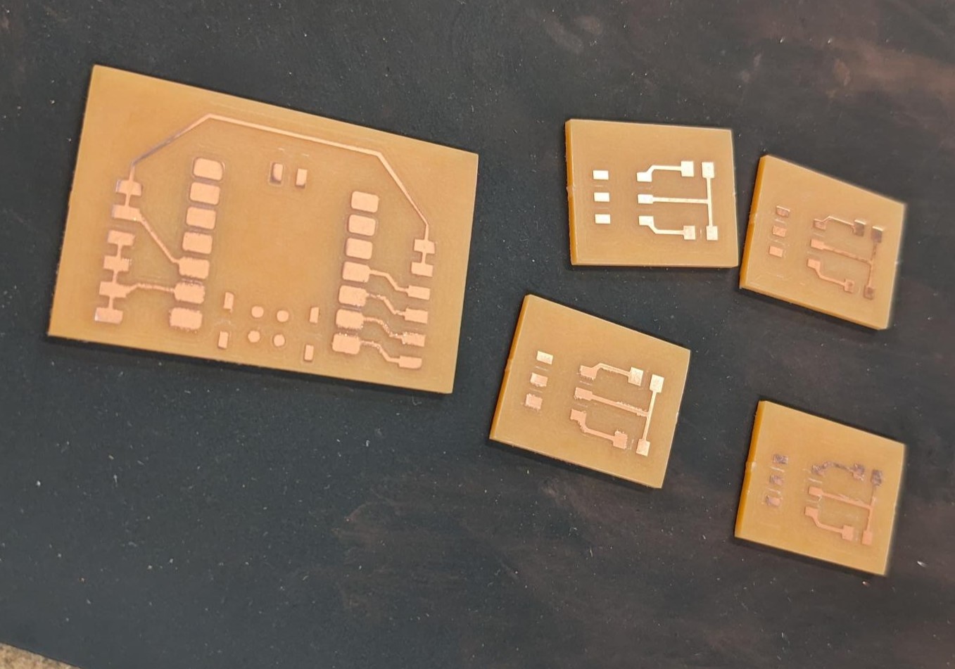
After sanding the traces down to remove the residual copper, I soldered the boards with visible light phototransistors, 10kOhm resistors on the photo boards, and female horizontal pin headers. I did have one snafu where I wasn't paying attention to the board orientation and soldered my XIAO facing the wrong way. But the hot air gun made it quick to remove, clean up, then re-solder facing the correct direction. It was at this point that we tested one of the photo transistors for the group work assignment before I cut wires to connect everything to the proper pins.
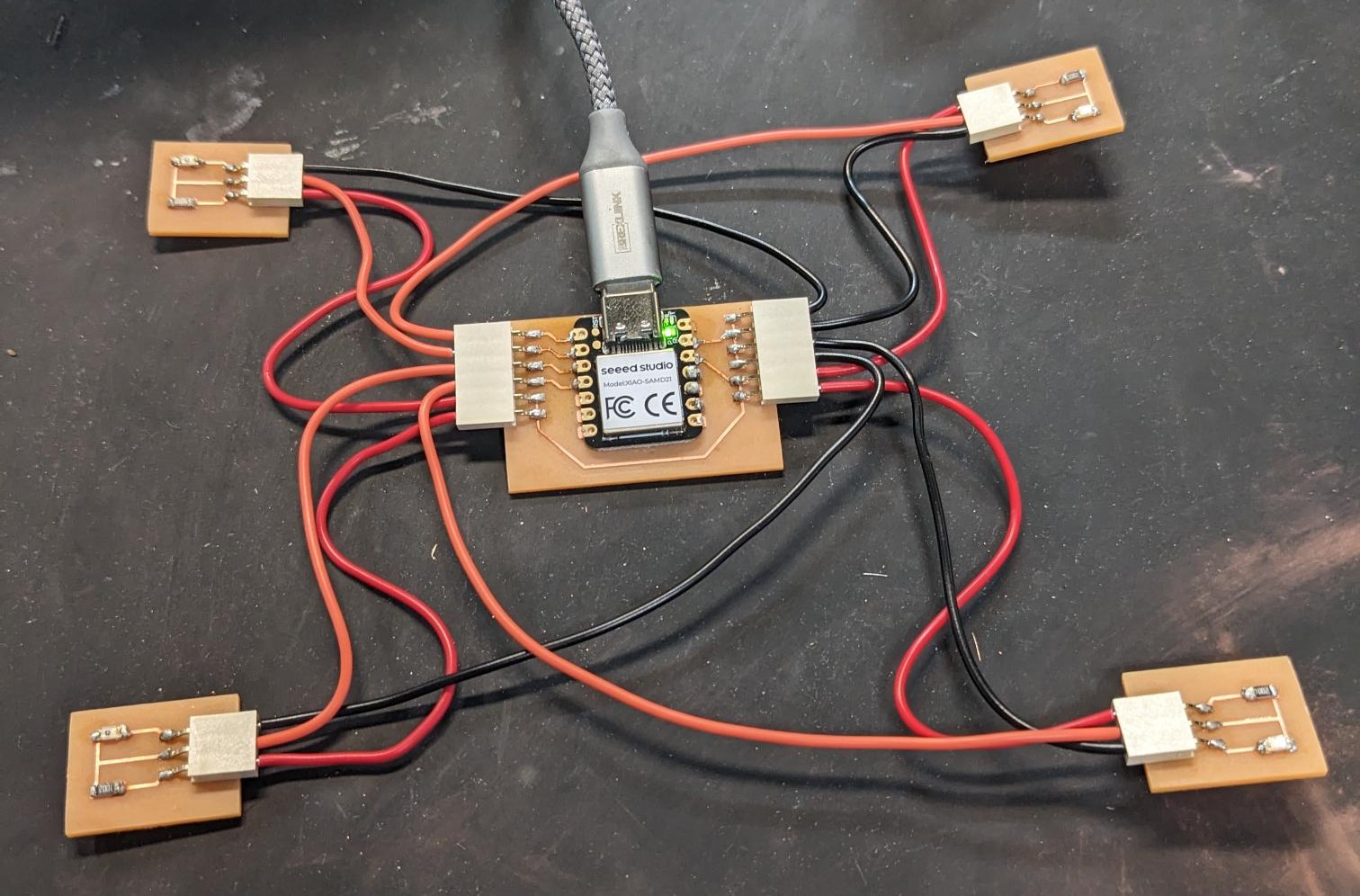
The programming this week was also super simple, it was really just plug and play (a nice improvement over my trials and tribulations trying to program the SMD SAMD21 from Week 6). I did have to take a moment to go back to the data sheet to figure out which analog pins corresponded with the actual pin number of the SAMD21, but once that was figured out my code was quite easy to write. I essentially just read the voltage between the resistor and the phototransistor (which changes based on the light level), and then do a slight bit of formatting/processing to get the output to read nicely. As a result all four 'distributed' phototransistors are labeled appropriately as top right (TR), top left (TL), bottom left (BL), and bottom right (BR). Each output block displays the raw analog reading as well as a threshold to whether the lighting would qualify as darkness, ambient, or bright light. A video of the code operating is below along with the design files for this week.