Networking & Communications
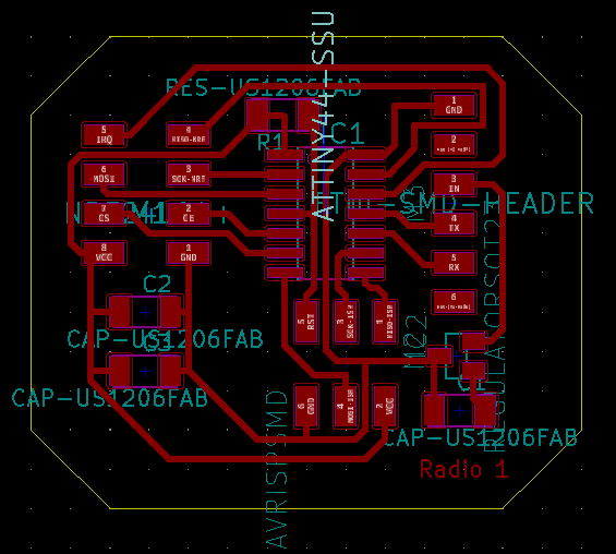
Step 2: Draw a schematic for your radio board following the steps outlined in the KiCad demo video but using the fab library components listed below and the layout shown in the photos. I used the following components from the fab library:
- ATTTINY44-SSU
- AVRISPSMD: 2x3 pin header
- FTDI-SMD-HEADER: 6 pin header
- NRF24L01+: radio, use footprint fab:fab-2X04_THRU
- REGULATORSOT23: 3.3V regulator
- RES-US1206FAB: 10k
- CAP-US1206FAB: 0.1uF, 1uF, 10uF
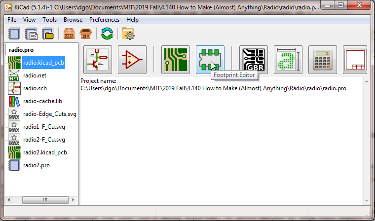
Pro tips: For some reason, the assigned footprint for the nRF24L01 (fab-2x04_THRU) didn't appear when I loaded the netlist from the schematic to the PCB. If you have this same problem, edit the footprint library using the following steps:
- Open KiCad's project manager and then click on the PCB footprint editor button.
- Navigate to the fab -> fab-2X04_THRU footprint. Double click on this footprint to open it up in the editor. No footprint will appear.
- Try double clicking on the next footprint, fab-2X05SMD. This time, you should see the footprint in the editor.
- Right click on fab-2X05SMD > Save As... and save a copy as fab-2X04_THRU. Feel free to write over the existing file; it's not helping us anyway.
- Now when you double click on the fab-2X04_THRU footprint, you should see the same footprint as the fab-2X05SMD.
- Right click on fab-2X04_THRU > Edit Footprint.
- Delete pads 9 and 10, and rearrange the pads to match the pad order photo.
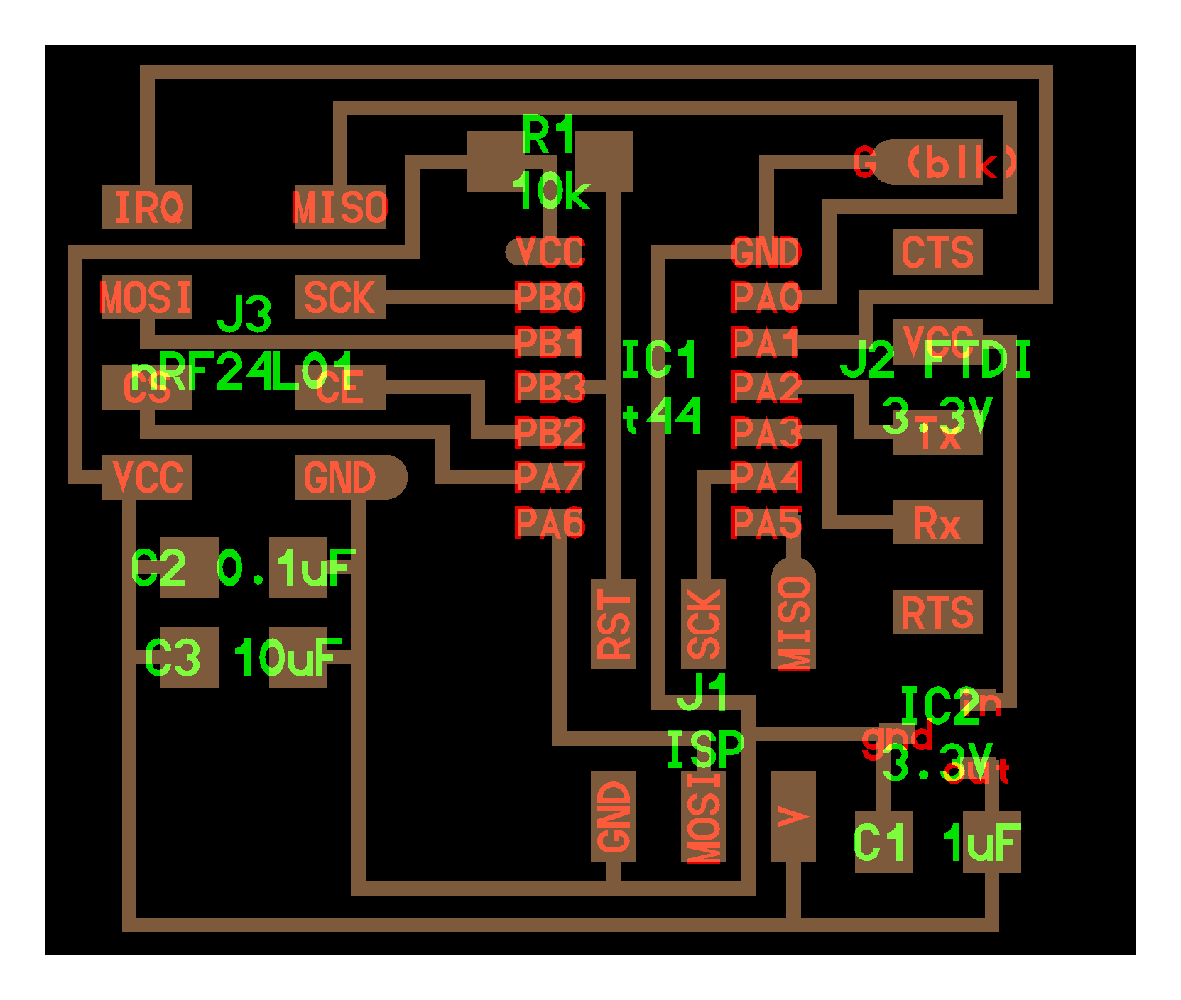
As always, make sure you leave 2-3mm between your outer traces and the edge of the and 5-6mm between the FTDI footprints and the edge of the board so that the black part rests on the board, reducing mechanical load on your soldered joints. I also increased the track width from 0.25mm (too thin) to maybe 0.4mm. I've also found it useful to shift some of the not-to-be-exported PCB text so that it spills beyond the edge cut so that no edge cuts accidentally disappear in mods. Finally, don't forget to perform a design rules check to make sure everything's connected. Even then, I missed a trace between the 1uF capacitor and power, so I had to go back and solder a jumper wire on both boards.
Step 3: Export your traces and edge cuts for milling! I added "Radio 1" and "Radio 2" text and exported traces for each. This was helpful for me to differentiate between my transmitting and receiving boards.
Step 2: Solder the components to your board.
Step 2: Connect the transmitting board to your programmer AND to power.
Step 3: Open a terminal in the folder with the saved files and run "make -f tiny44_tx.make ProgrammerName." The relevant programmer name can be found in the makefile. Repeat process for the receiving board.
Pro tips: Electronics are like small animals that desperately want your attention. I finally finished my FabFTDI this week after having built the wrong one last week. I ran into a million and a half problems programming, but once I pretended not to care and started doing something else, the problem would magically resolve itself. I'm not a fan of this method of working, but I'm glad things started working in the end.
Step 4: Download and run CoolTerm. Connect both radios to your computer, and open one terminal for your transmitter and one terminal for your receiver. Connect, and watch the magic!
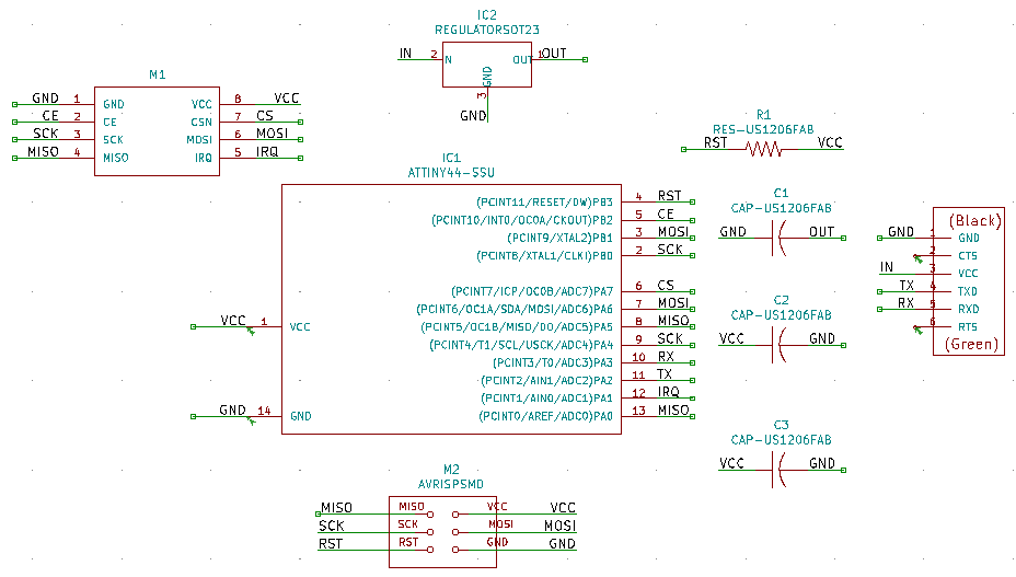
My KiCAD schematic
Footprint library
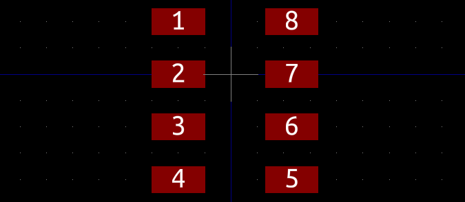
Pad order
My nRF24L01 PCB
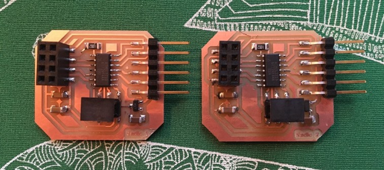
Radio 1 & Radio 2
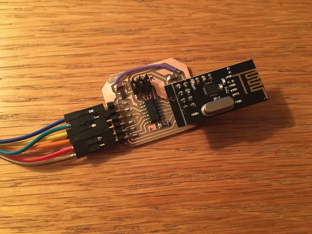
Final assembly
Transmitting!