Electronics Design
Mission
The aim of this week is to learn how to design our own circuits using available software tools, as well as learn how to program them.
Group Project: use the test equipment in your lab to observe the operation of a microcontroller circuit board
Individual Project: Redraw an echo hello-world board,
- add (at least) a button and LED (with current-limiting resistor)
- check the design rules, make it, and test that it can communicate
- extra credit: simulate its operation
Individual Project
Ok, this is definitely building on what we learned from the milling week, however it demands much more.
My Process
- Design a board using an EDA (Electronics Design Automation) tool
- Mill and stuff the board
- Load a bootloader onto the Microcontroller (MCU)
- Hook it up to an Arduino IDE and program it to do something
My Files
Resources
I really appreciated Zach’s recitation on KiCad which I studied carefully.
Designing the Board
Download EDA software to use. I decided to use Kicad, which is a free and multi-platform tool. It’s a little bit tricky to download it for the Mac, in that you need to throw some helpful libraries in an Application Support folder, but it doesn’t work well by just dragging the kicad folder into it. I ended up having to go in and manually point to the libraries and symbols. I also needed to add the “fab” library, which is more specific to the parts we have in our lab.
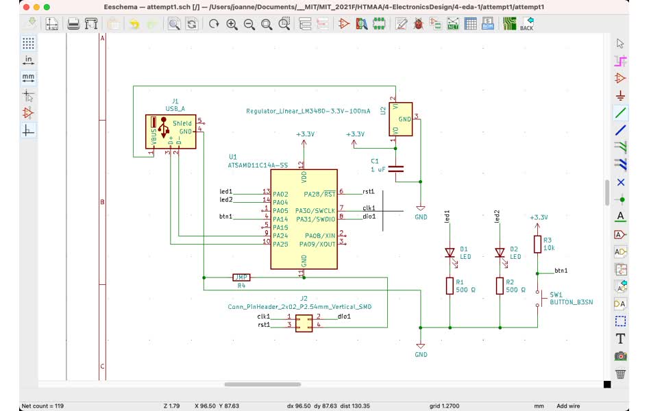
Once I had Kicad installed with the libraries I needed. I could start designing. It turns out that you need to specify the design from 2 perspectives. You need to design in a schematic view, which describes the electronic logic of the board. Then you move to the PCB layout view, where you actually desig the layout of your board, which follows the rules of your schematic.
For the schematic, the first thing I did was press ‘a’ to add symbols to the canvas. I needed to look around to find symbols I needed. After that, you need to draw wires between the pins. The pin layout in this view doesn’t match what’s in real life, so you have to go by the labels you can see. Use ‘w’’ to draw wires. Make sure that the lines actually connect to the components. If there is a gap, they’re not connected. Wires in this view can cross each other. You’ll know if they’re connecting by seeing a big circle which symbolizes a junction. Once you have everything wired up, you need to match the symbols to actual ‘footprint’ descriptions of the components you want to use. Footprints describe the physical layout of the components! Then you export a net file which you will import into the PCB view.
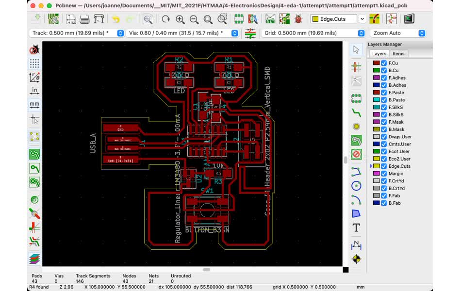
In the PCB view, this is where you import your net file. When you do, you see a messy clump of components called the “rat’s nest.” This is a pretty gross name in my opinion, which maybe makes it sound even more unpleasant. Anyways, you need to untangle it. The reason it’s all clumpy is because all your logical connections from the schematic are ported over. You need to layout out the components nicely now, and these logical connections need to be converted into real physical traces to mill.
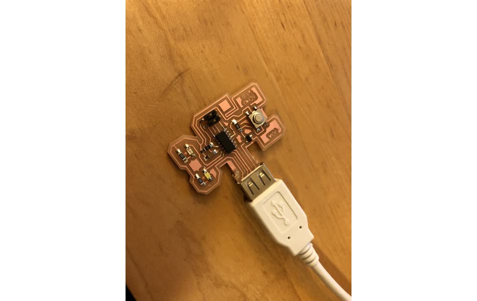
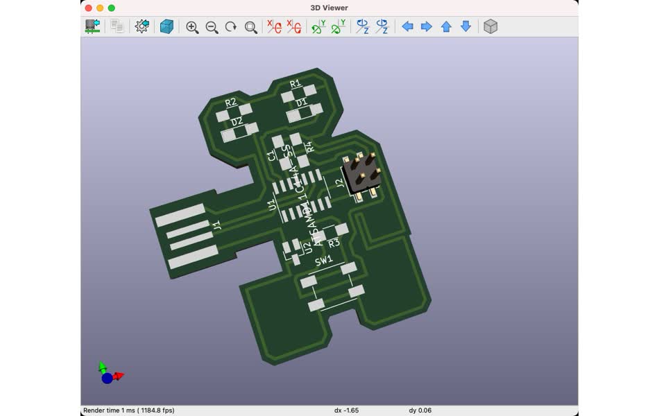
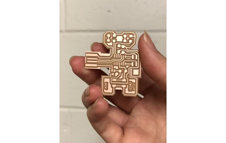
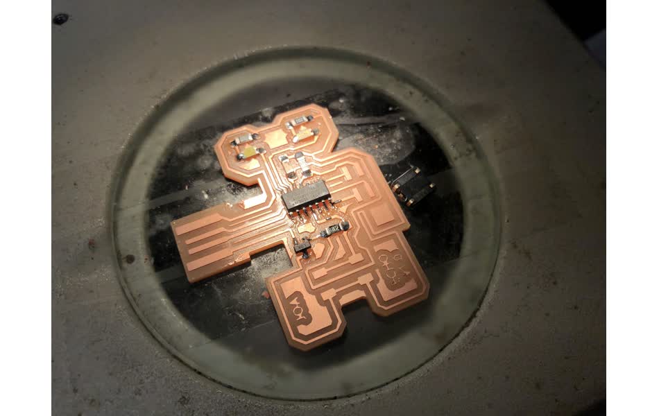
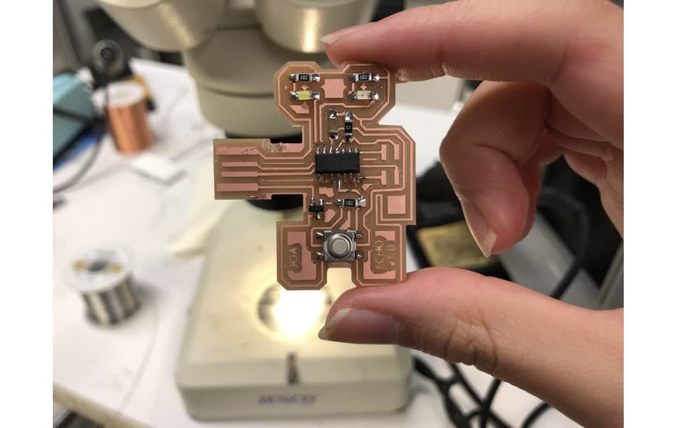
For me, I had decided to add two LEDs in my schematic (double the fun!). So I decided I wanted to make them into eyes. I got the idea to make a robot, and then the Disney robot Wall-E came to mind. I decided to make Wall-E with this. Yes, you need to use a little bit of creativity to see the resemblence, but I swear I looked at a picture of Wall-E to get the shape! I tried to organize the components to minimize the number of crisscrossing logic lines. I figured this would help to minimize actual trace collisions. This whole thing is a puzzle game, so I was glad I did this earlier in the week so I wouldn’t stress while doing it. I’m very proud that in the end, I figured out a layout that followed the shape of Wall-E and only needed 1 0 ohm resistor as a ‘jump’ resistor. This means I just needed to do one cross-over on my one-sided PCB. ![]()
Adding a jump resistor required that I go back into the schematic to add the resistor and describe how it will be connected to the other components. I then had to make a new .net file and import this into the PCB view. Luckily there’s a button to simply update the PCB from the schematic so you don’t eliminate all of your hard work that you already put into designing traces. I ran the debug tool to check for errors, and initially found some things. It complained about traces being too close to the board edges, which was weird when I hadn’t sketched them in yet. It also complained about some components not being wired up. It turns out I had an error in my schematic, so I iteratively went back and forth until I didn’t have this error anymore. I then selected the outline layer and drew around my design to create the board’s edges. Once I did, I didn’t have any more warnings or errors. Great! You can enjoy your work by looking at it from the 3D viewer in KiCad. Now if you’re happy, you can export the file as an SVG.
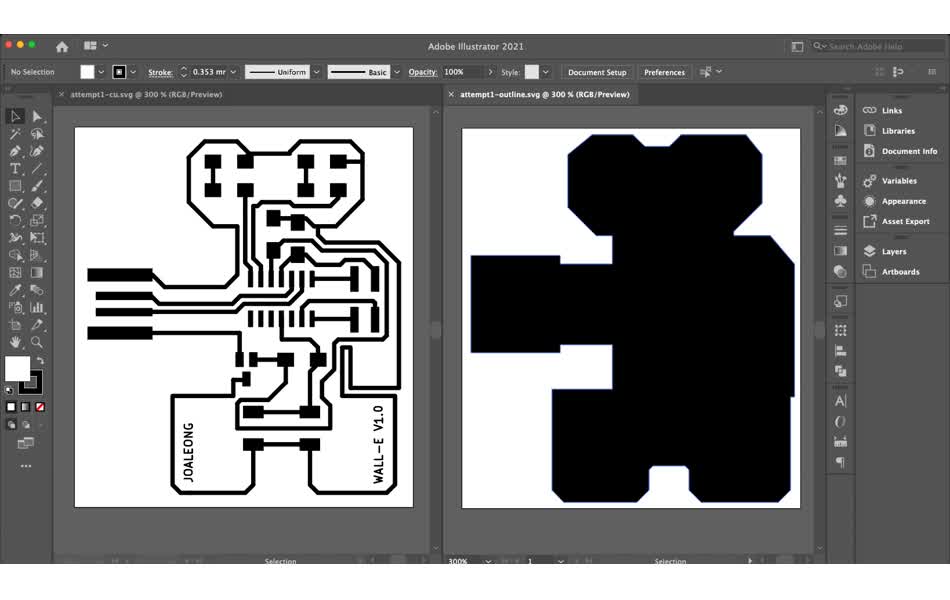
Now you need something like Illustrator to actually put things on two layers. You put the copper traces down in one layer, and you put the outline in the other. Make sure that they are not shifted, so that they correctly align when you go to mill it. The copper traces don’t need any modification. However, you do need to select the outline lines, and fill it in as a shape! Finally, it seems like Mods doesn’t like SVGs that come out of Illustrator (cannot import it correctly). So export this instead as a PNG to import into Mods,
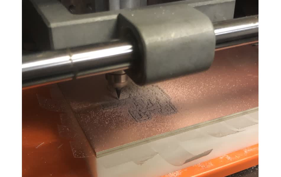
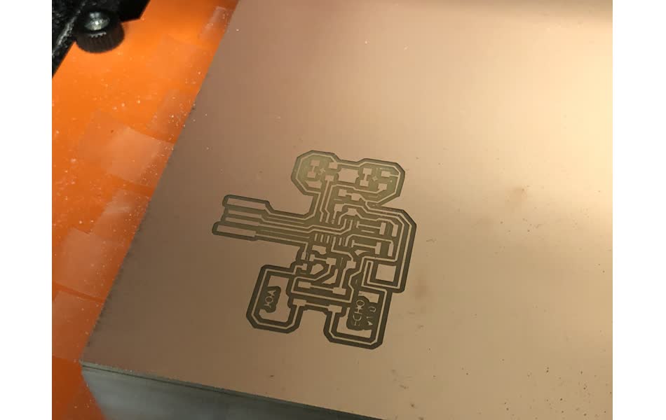
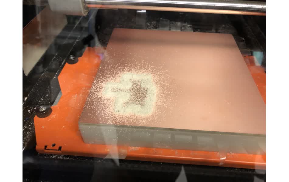
Milling and Stuffing the Board
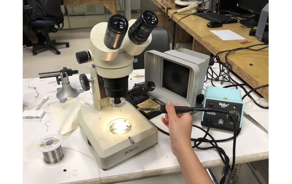
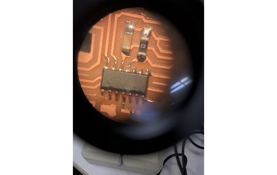
I followed the steps we had learned before. Fortunately, I managed to do this perfectly and Wall-E was born! You can see that the words I added were not designed well to come out pretty on the PCB. I’ll perfect that for next time. Stuffing the board required patience as usual. The MCU was the hardest thing to put into place. I put it down, and wasn’t happy with the placement. I wiggled it, and ended up ripping off on my copper pads! (Oh no!) Luckily, this copper pad wasn’t wired to anything, so I figured I could keep going. The rest of the components were easier to do. This time around, I learned how to use the microscope and I can say that it was very helpful. I couldn’t see at first that some of the pins of my MCU were not connected properly, but under the microscope this became a little clearer. (Still took some finessing of the microscope to see it as you have to change the strength sometimes if you’re putting your board at an angle to take a look.)
Bootloader
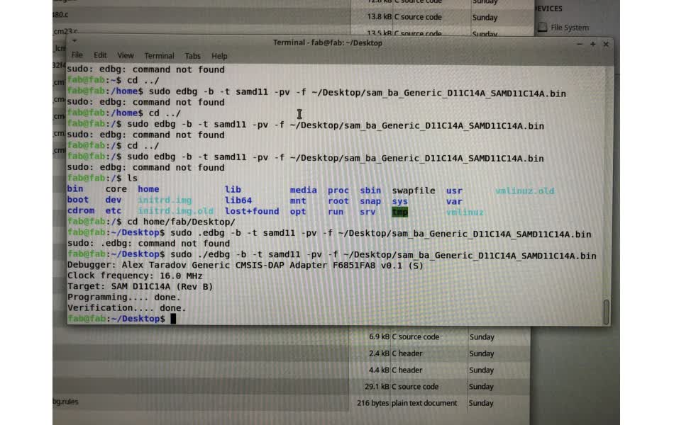
I started on the process of getting pyOCD and the binary file that would be loaded onto it. However, I learned that edbg was already available on the lab’s Linux machine. Therefore I hooked up my board to Zach’s converter and plugged it in as you can see in the photo. I found that the executable for edbg was on the Desktop, so I had to navigat there in the terminal. Then I typed in the following command into the terminal… and this worked! Yay!
sudo ./edbg -b -t samd11 -pv -f ~/Desktop/sam_ba_Generic_D11C14A_SAMD11C14A.bin
Programming the Board
I now needed to setup my machine so I can program the board. Essentially there were a few crucial steps.
- Download the Arduino IDE. I had this alreayd, but it didn’t seem to work anymore so I downloaded a new version.
- Go to Arduino > Preferences > Additional Board Managers URLs and add the following JSON URL as a new list item
https://www.mattairtech.com/software/arduino/package_MattairTech_index.json - Got to Tools > Board > Boards Manager and get the
mattairtech SAM D|L|C core4, Now you’re ready to select your board from Tools > Ports. Mine was listed as a mattairtech board.
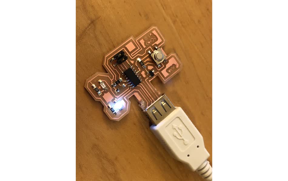
Once this is in place, you can write a program like any other Arduino one! I made mine light up differenty based on the button press. Verify your code and then with your board plugged in you can upload your program to the board and have fun! ![]()