Electronics Design

This week, we are returning to electronics. From the previous week where we simulated some simple code on a pre-made development board to achieve some kind of output, this week we are building the microcontroller breakout board itself. Essentially we will be building a [insert your favorite dev board name here, e.g. arduino uno, pi pico, etc]. As with every week, we begin with the group assignment and training for lab tools relevant to this fabrication assignment.
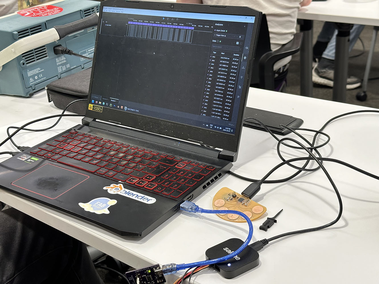
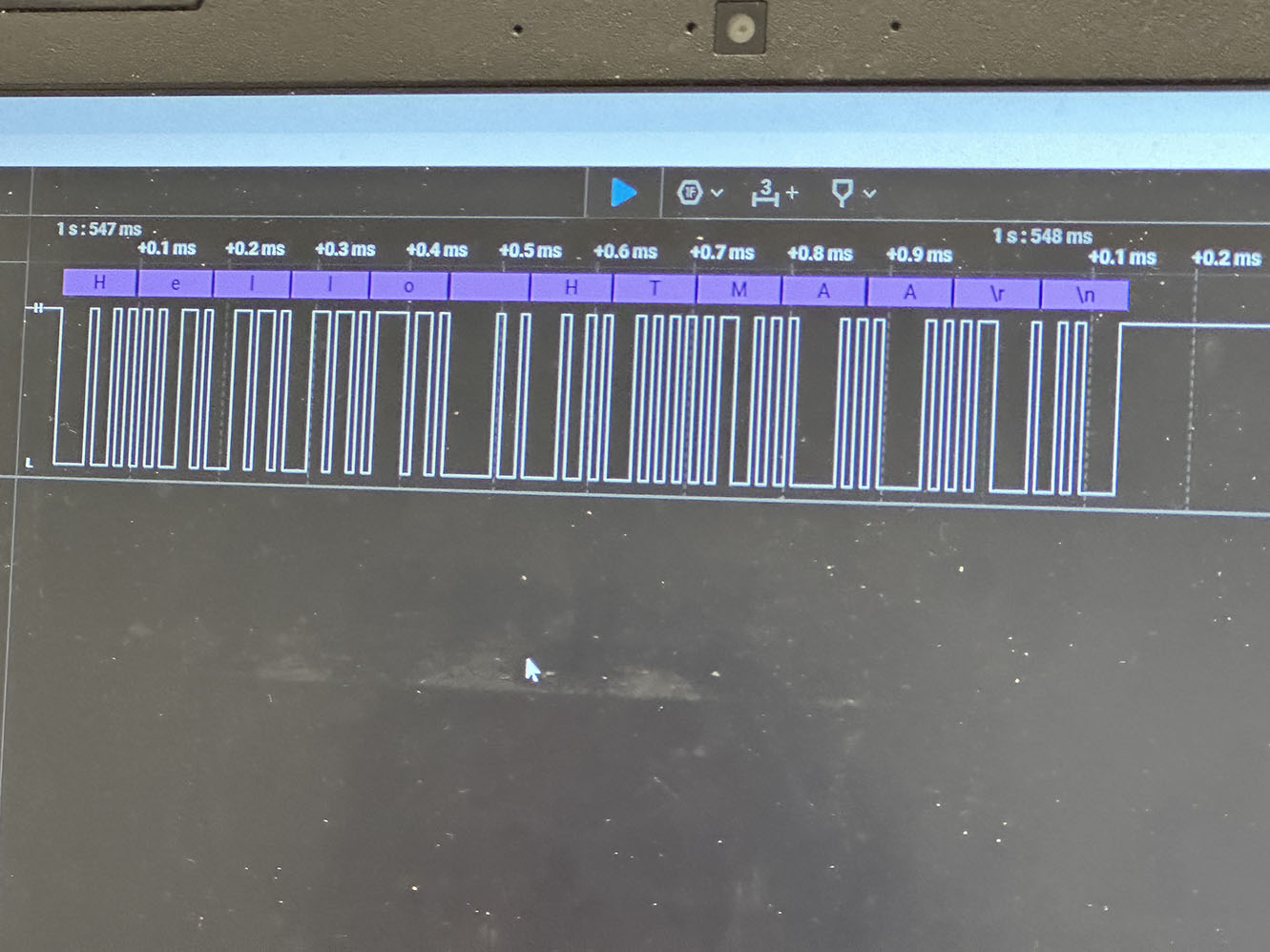
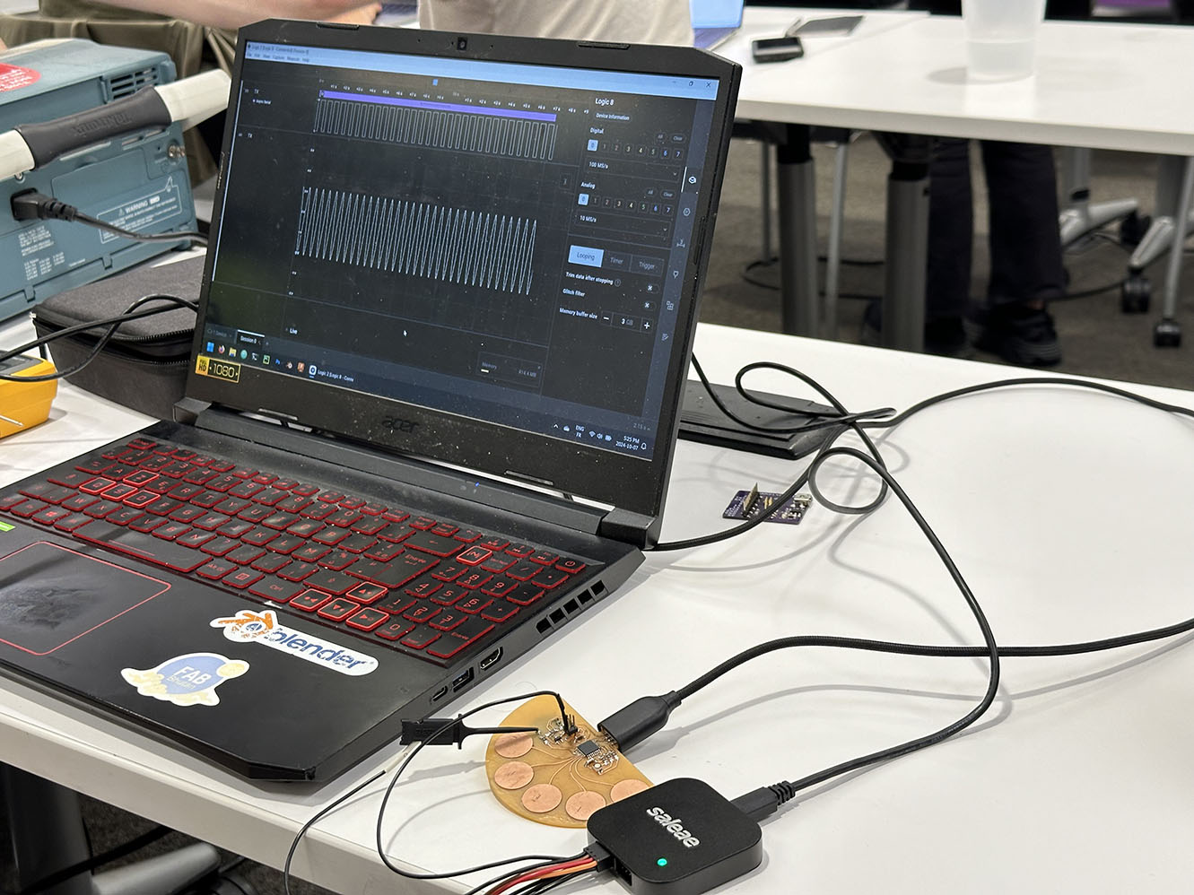 The main tools for this week are debugging tools that can help identify problems with the circuitry of our development boards, such as multimeters, oscilloscopes, and logic analyzers. Having no prior experience with PCBs, I'm sure I will become very familiar with these tools in the near future. I have used multimeters and oscilloscopes before; however, I have never heard of a logic analyzer so this is the focus of my group work. The main lab tool here is a Saleae logic analyzer. This handly little device also doubles as an oscilloscope. The figure to the left shows the oscilloscope function of the Saleae, and below are figures showing the logic analysis. This is neat - the software has presets to decode the logic for ease of viewing. Here the decode is set to ASCII and a "HELLO HTMAA /r /n" shows up. The /r is a register return (held over from the era of typewriters), and the /n is a new line.
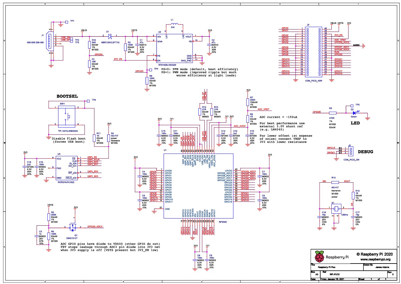
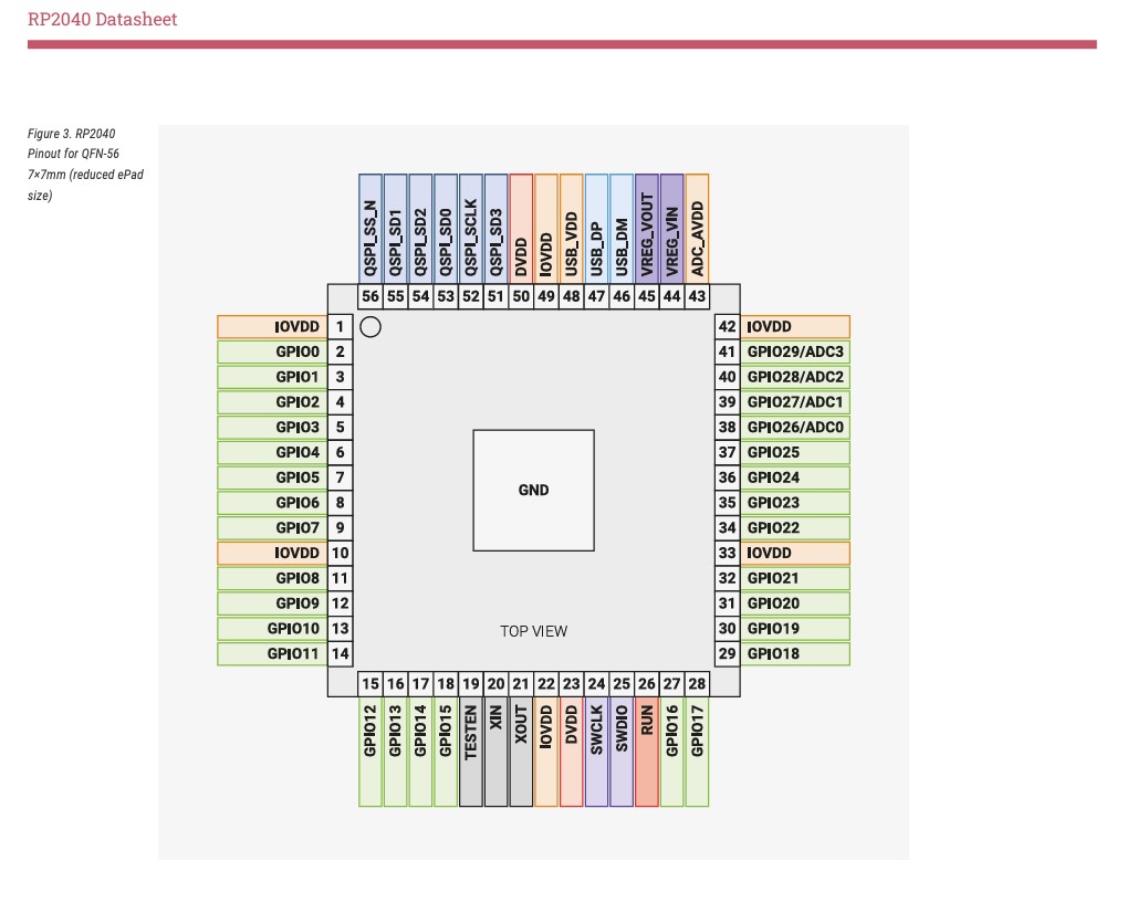 These tools will be helpful once I actually make my PCB, but first I need to design it. This task seems daunting, but in reality it is rather simple when making use of tools like KiCad. The microcontroller I want to use for my development board is the RP2040, similar to the controller on the Pi Pico from the Embedded Programming week. The pinout schematic for the RP2040 is shown to the right. This chip has a lot of versatility, and a lot of GPIO pins to make use of. One key thing here, however, is that to fully support this chip in a development board, much work needs to go into the board infrastructure. Take the figure below of the Pi Pico as an example of a fully supported board for the RP 2040. I will not pretend to fully understand the design decisions that went into this board.
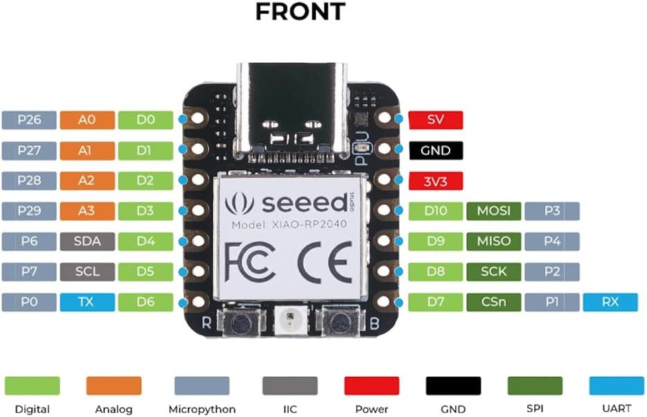 Because of the complex engineering of the board, I will opt for a slightly more user friendly board to begin with - the Xiao Seeed RP2040. This board features the timing and reset functions built in, and I can customize it to be used for the Opti-phone final project needs rather easily. The pinout diagram for the Xiao is shown to the left. The main limitation of the board is that, from the 32 pins of the original RP2040, only 11 are utilized here, meaning the entire chip is underutilized in general. For this week, and for the Opti-phone actuation controls, this will be ok as a first pass. With the board identified, let's begin the design.
The first step in KiCad (after importing and assigning libraries), is to place the board and create global labels for the pins. This will help keep the schematic clean and organized moving forward. After the labels, one of the servo connections is created. Each servo motor will require three connections: power, ground, and an IO slot. This will be tedious to channel in the next step, but thats a problem for future Kyle. Below is the Global Label attributes for the Xiao and one of the servo connections, to be repeated several times.
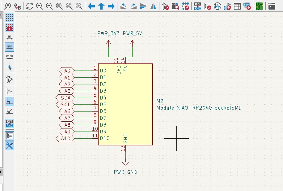
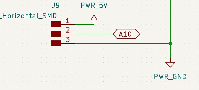
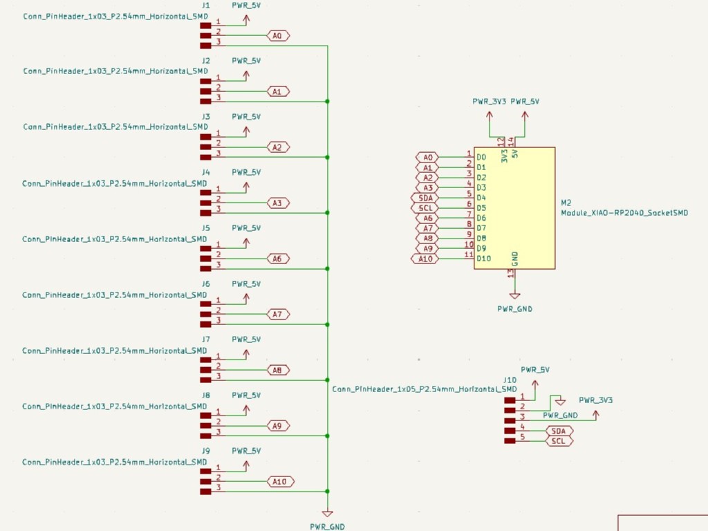
The pin assignments for the servos is the same across all of the analog in / digital out pins on the board (marked with an A##). Note that there are two pins marked SDA and SCL. The SDA (serial data) pin is used for serial communication of data between boards, and the SCL (serial clock) carries the clock signal. These will be used to gather the incoming ASCII commands from a connected device / computer, but for right now they will be broken out into pins of their own. The servos will therefore be allocated to pins A0-A3 and A6-A10. below the servo pinouts are shown, alongside the SDA/SCL breakout.
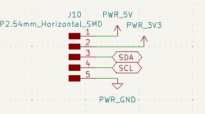
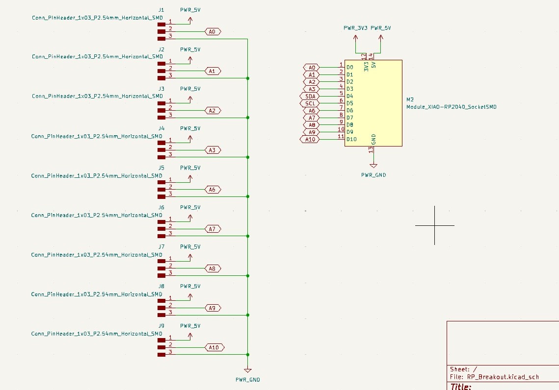
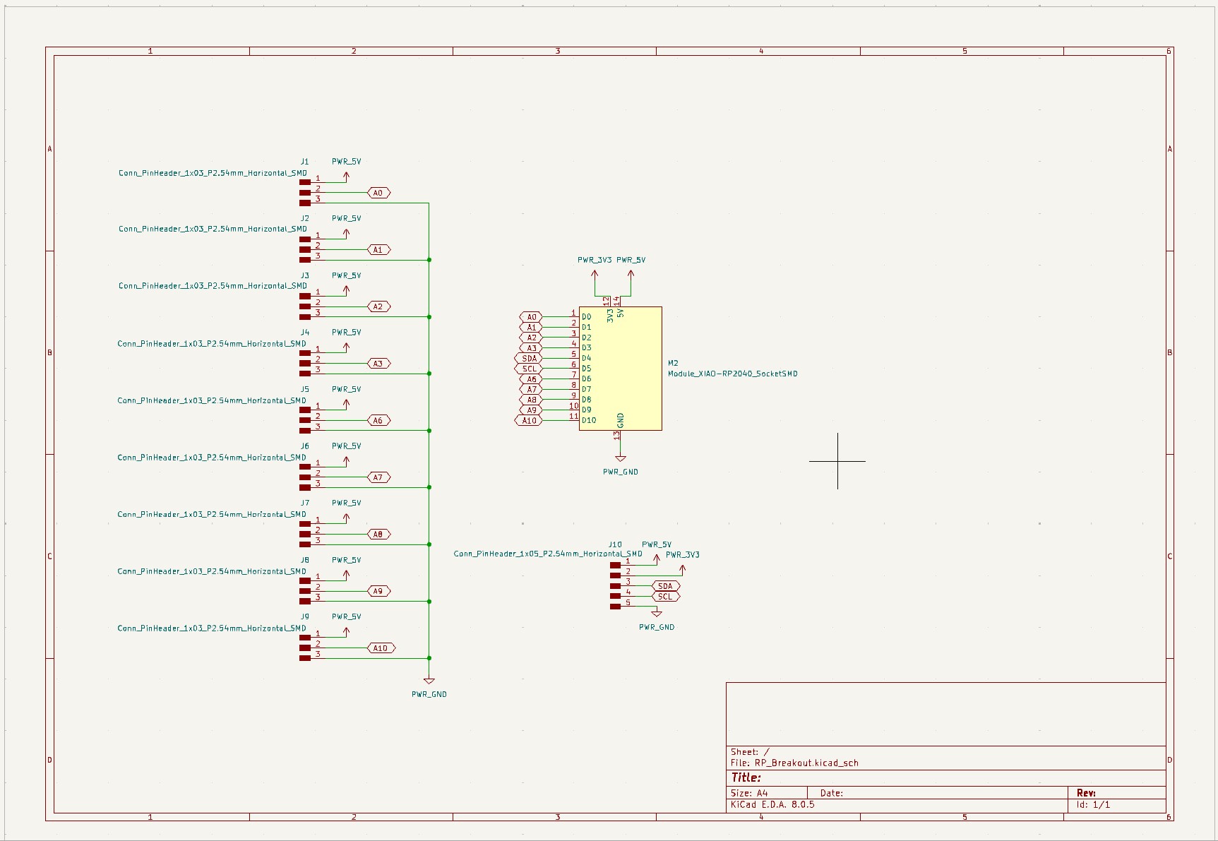
This now completes the board, with the final schematic shown below.
Now it's time to design the channels for the copper. To do this we transition to the PCB editor in KiCad and import the footprints and connections from the schematic. A few minutes are needed to sort through the piled mess it presents you with, but eventually you get something that looks like this:
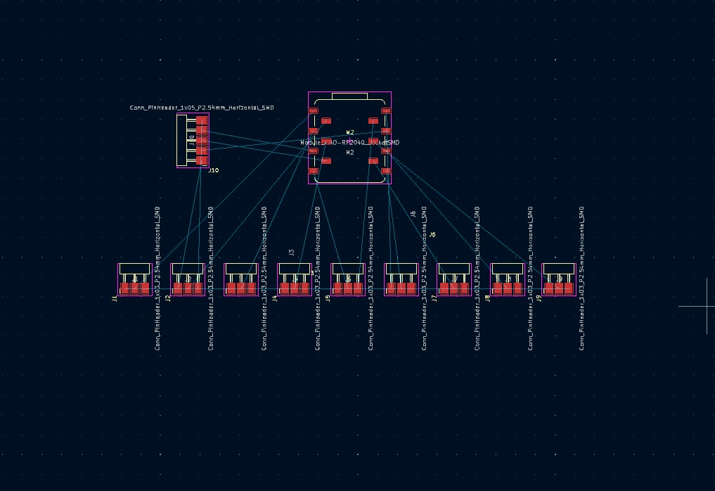
This is great. All of the connections are shown, and it even shows you where some overlapping wires exist to clean up in the schematic. From here I'm opting to make use of both the base and front copper for this board given the number of power connections I need. I'll allocate the top copper surface for my power and ground connections (shown in the PCB editor as red), and the base copper for my data connections (shown in blue). Below are both of those connections drawn out.
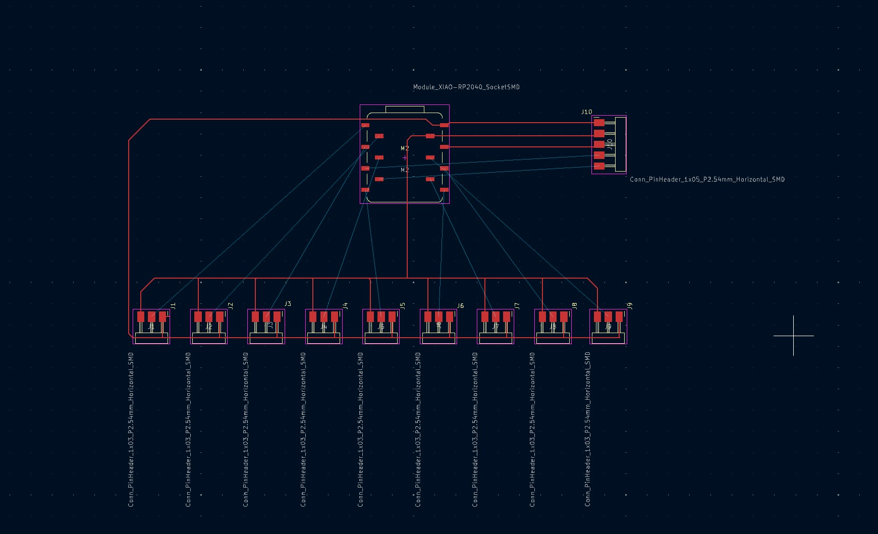
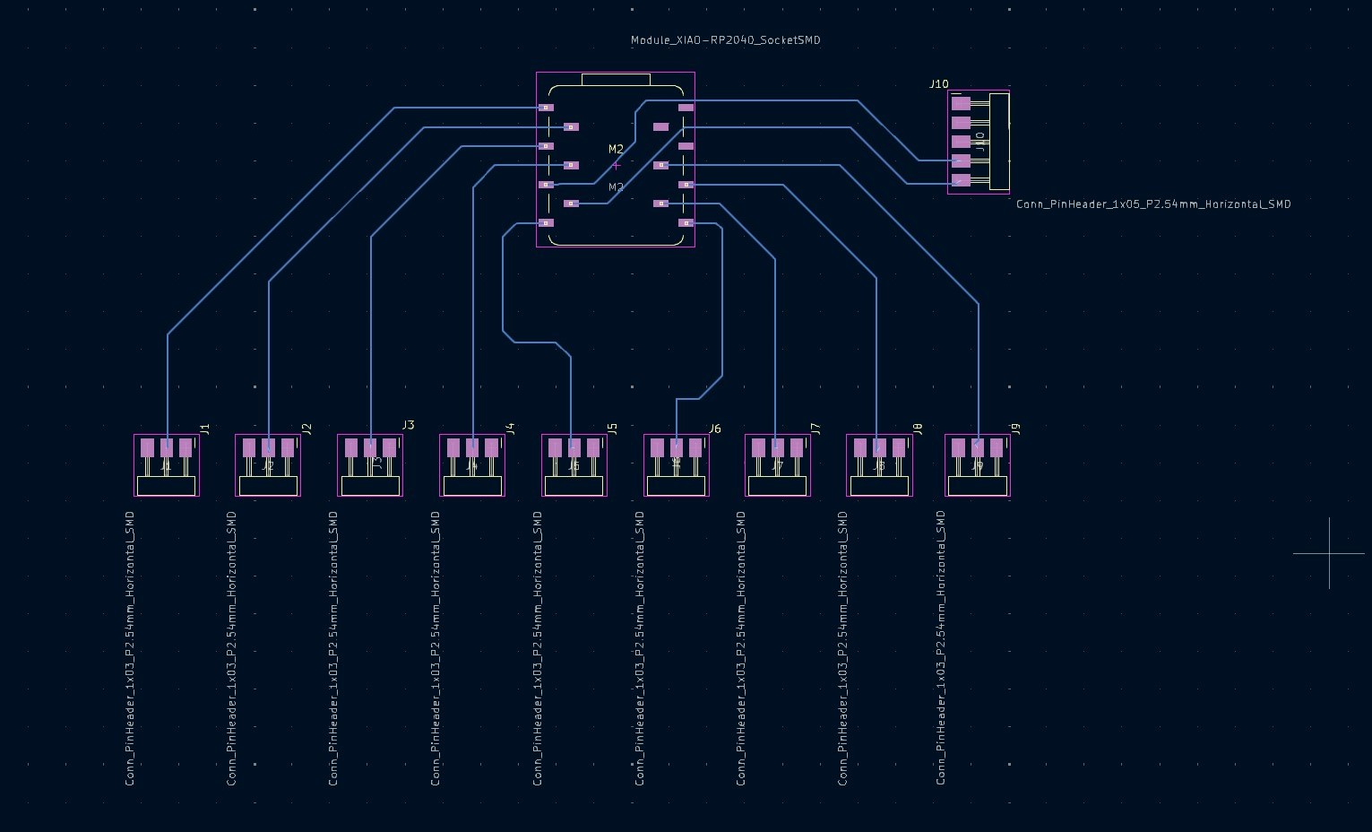
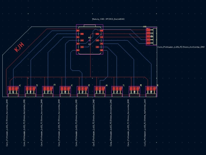
During the drawing process I realized the SCL and SDA ports needed some rearranging on the board to make the wiring a bit more concise. This is fine, the back and forth of this design flow is similar to a lot of other engineering design problems. These connections, overlaid, with the board cutout (shown in white) is shown below alongside the final schematic for the controller. This concludes the week, and it was good! I was always a bit intimidated by PCB design, but KiCad is an excellent tool that enables a lot of freedom to create very practical chips. I wish there was an easier way to be creative with the designs in KiCad, but other tools, like SVG-PCB, can enable that rather easily. This development board will make my final project a bit easier to debug as well hopefully, and I'll be updating the final project page with this week's work shortly.
Below are also my KiCad files for this build, should you want to make this one yourself as well.
- Download KiCad Schematic File
- Download KiCad PCB File
- Download KiCad Project File (you will need this to make the shcematic and PCB files work)
- Download KiCad Project Libraries (you will need this to make the others work)
